FS2. Clocks, pulsed latches and storage cells: the exam way
This is the exam way of FS2: each part as you would write it on the paper, with what to recognize, the lines to write, what to draw, the trap to watch and the answer. Every part keeps the anchor it has on FS2, so the switch at the top of the page takes you to the same part’s full solution. The methods are three cards of the playbook: clock generation, pulsed latches and storage cells. The six harder variations stay on FS2 only, at the end of each family: clock generation, pulsed latches and storage cells.
The clock. The past finals gave 180 minutes: FN12 for 200 points, 0.9 min a point, and FN19 for 250 points, 0.72 min a point. So FN12-7a’s 15-point sketch has about 14 minutes, and a 10-point FN19 part about 7. (The midterms ran at 30 s a point.) PS5 is a problem set and gives no points: each of its two parts is budgeted here by analogy, as a 10-point design part on a final, about 8 minutes.
1. FN12-7: a local clock generator (15 points of 30)
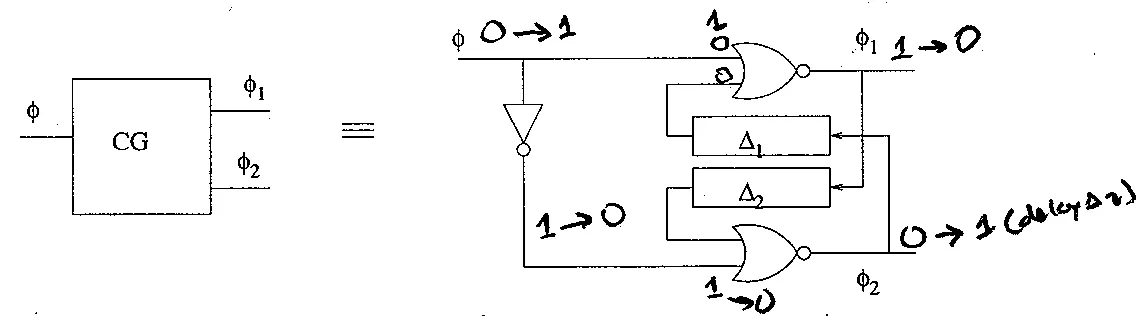
FN12-7, p10. Consider the “local clock generator” circuit shown below, used to generate two clock phases locally from a single-wire global clock. The delay blocks (labelled with and ) could be implemented with an even number of inverters (for example).
FN12-7’s local clock generator (p10, redrawn): CG ≡ two NORs and an inverter. Each delay block takes the other phase: takes φ2 into φ1’s NOR, takes φ1 into φ2’s NOR. Below, the paper’s φ with empty rows for φ1 and φ2.
The exam’s own figure (FN12-7, p10)
Part (a): sketch φ1 and φ2 (15 points)
FN12-7a, p10. Sketch the and waveforms for the waveform shown below. Ignore the gate delays of the inverter and NOR gates but indicate the and delays on your sketch. (15 points)
Hint
Recognize. Clock generation: cross-coupled NORs with delay blocks, “sketch the waveforms … indicate the delays”. About 14 minutes (15 points at FN12’s 0.9 min a point); the walk takes five, the rest goes on a clean sketch.
On the paper.
- ,
- NOR: any input 1 → 0 at once; 1 only when both inputs are 0
- Start, φ = 0: → φ2 = 0 → φ1 = 1
- φ ↑: φ1 ↓ at once; is still 1 for → φ2 ↑ at
- φ ↓: φ2 ↓ at once; is still 1 for → φ1 ↑ at
- Check: never both high (one NOR always has a 1 on its direct input); gives φ1 = φ̄, φ2 = φ
Draw under the paper’s φ: φ1 low through each high pulse, φ2 high from after each rising edge to the falling edge; φ2 low through each low stretch, φ1 high from after each falling edge to the next rising edge. Label each gap after a rising edge and each gap after a falling edge .
Watch out. Only the rising edges wait: a phase is not a delayed copy of φ or φ̄, because it falls at once. And sits after φ’s falling edge (it delays φ2, the phase φ1 waits for); swapping the labels loses the marks for them.
Answer: φ2 is high from after each rising edge of φ to the falling edge; φ1 is high from after each falling edge to the next rising edge. Both phases are low for after every rising edge and for after every falling edge.
2. FN19-5: a clock chopper and a runt pulse (22 points)
FN19-5, p11. Consider the clock chopper circuit shown below. The delay block (labelled ) can be implemented with an even number of inverters.
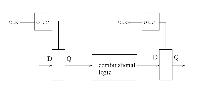
FN19-5’s figures (p11, redrawn). (a) The clock chopper: CC ≡ a NOR of φ and φ inverted and delayed by Δ. (b) Two clock-chopped latches, each clocked by its own chopper, from CLK1 and CLK2, with combinational logic between them.
The exam’s own figures (FN19-5, p11)

Part (a): the widest pulse (10 points)
FN19-5a, p11. Consider two clock-chopped flip-flops separated by combinational logic as shown below. Assuming that the combinational logic represents a fixed delay of 200 psec and there is skew between CLK1 and CLK2 such that CLK2 arrives 100 psec earlier than CLK1, what is the maximum value (the pulse width of the chopped clock) can have and still ensure correct functionality? Assume that the latches have a hold time of 50 psec on their closed clock edge. (10 points)
Hint
Recognize. Pulsed latches: “maximum value Δ … hold time … on their closed clock edge” is pulsed hold. About 7 minutes (10 points at FN19’s 0.72 min a point).
On the paper.
- Chopper = NOR(φ, φ̄ delayed by Δ): a pulse Δ wide after each falling edge
- Identical choppers, so the pulses are offset by the skew: ps (CLK2 early)
- No given: take it as 0 (say so)
- Hold at the closing edge:
- ps
- Check: with no skew, ps; the early CLK2 buys exactly its 100 ps
Watch out. CLK2 early makes negative: adding the 100 ps as a late skew gives 50 ps. Hold counts from the pulse’s closing edge, not its opening.
Answer: ps (with , which the paper does not give).
Part (b): the chopped clock through a loaded inverter (12 points)
FN19-5b, p12. Assume that this chopped clock with the pulse width calculated in (a) is driven from an inverter with a load capacitance of 200 fF. The inverter is sized in a technology with a FO1 delay of . Assume a gate capacitance of . Sketch the waveform of the clock as received by the latch. What will be the “height” of the pulse? What problems might this present? (12 points)
Hint
Recognize. Pulsed latches, the distribution move: a driver, a load and “the height of the pulse” mean a runt. About 9 minutes (12 points at 0.72 min a point).
On the paper.
- fF
- ps (50% point)
- : a runt
- RC with its 50% point at : ps
- Height
- Shape: from 0, rises as for 250 ps to , then decays with ps
- Never crosses : the latch may never open, or opens weakly and late
- (a) caps the pulse, so speed the driver: ps needs fF (10 µm) for just , about 66 fF (33 µm) for 90%; or chop at the latch
Draw the dashed 250 ps command pulse and, under it, the rounded bump that peaks at at 250 ps and decays; mark to show it is never reached.
Watch out. Taking itself as the time constant gives (the unofficial 2019 solution’s boxed number); the course’s delay is the 50% point, so . Write your convention down. Widening the pulse is not a cure: (a) caps it.
Answer: The latch receives a rounded positive runt about high, because the driver’s delay into 200 fF (417 ps) is longer than the 250 ps pulse. It never reaches , so the latch may not open at all, or opens weakly and unpredictably. Fix it with a faster driver (10 µm only just reaches ; about 33 µm reaches 90%), or a chopper beside the latch.
3. FN19-9: a latch that cannot be written (10 points)
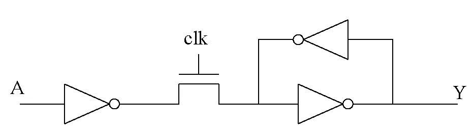
FN19-9, p21. Joe Engineer is designing a simple pass-transistor latch as shown below.
FN19-9’s pass-transistor latch (p21, redrawn): A drives an inverter, then a pass NFET on clk, then the storage node (unnamed on the paper; called X here), which drives the forward inverter to Y. The feedback inverter, always on, returns Y to X.
The exam’s own figure (FN19-9, p21)
What went wrong, and the fix (10 points)
FN19-9, p21. He finds that he is unable to write the latch; that is, when clk is high, Y is not affected by the value of A. What has gone wrong? How can this be fixed? (10 points)
Hint
Recognize. Storage cells: a latch at transistor level and “unable to write … what has gone wrong? how can this be fixed?” is a write fight. About 7 minutes (10 points at 0.72 min a point); the paper gives no sizes, so the numbers in lines 5–6 are an illustration you label as such.
On the paper.
- clk = 1: , so the logic is right; the fault is electrical
- The feedback inverter has no clock: on while writing, it holds X at the old value
- Writer: driver + pass NFET in series; holder: one feedback device
- Divider: ; writes only if crosses
- For example, inverters 2/1, pass 1 µm. Write 0: down , up → ✗
- Write 1: up (NFET pulls up weakly), down → ✗, worse; and X stops at
- clk ↓: the loop restores the old value; Y never follows A
- Fix 1: feedback weaker than the writer both ways: PFET < 1 µm, NFET < 1/3 µm, so it is made long
- Fix 2: stronger driver and a transmission gate (still a ratio)
- Fix 3, robust: gate the feedback with (a transmission gate or a clocked inverter in the loop)
Draw fix 3: the input switch on clk and a second switch on in the feedback loop, both transmission gates.
Watch out. A stronger forward inverter does nothing: its gate draws no current. Check both directions: writing a 1 through an NFET is the worse one.
Answer: The always-on feedback inverter fights the write: the driver through the pass NFET cannot pull the storage node past the forward inverter’s threshold, so Y keeps its old value, and the loop restores it when clk falls. Writing a 1 is worse (the NFET pulls up weakly and only to ). Fix it with a weak feedback inverter, a stronger driver with a transmission gate, or, best, feedback gated by so nothing fights the write.
4. PS5-Q2: a two-bit counter with a synchronous reset
PS5-Q2, p3. This is a small design problem. Design a two-bit wrap-around counter. The counter counts from “00” to “11” and then begins again at “00.” The systems takes as input a single clock and a synchronous input reset which resets the counter back to “00” when active. You may assume that reset arrives 20 psec after the rising edge of the clock. The clock is 50% duty cycle with 20-psec rise and fall times. The outputs are the two bits of the counter. Design your circuit for the fastest clock frequency possible and verify this maximum frequency of operation with Spectre. You do not have to layout your design.
The handout gives no points and no figure, and the Spectre search is beyond a written exam: the two parts below are the logic and the reset’s timing. The state diagram is drawn from the words.
PS5-Q2’s counter as a state diagram added, drawn from the handout’s words: the states are , and R is the handout’s reset. With reset low () each rising clock edge counts 00 → 01 → 10 → 11 → 00; with reset high () every state goes to 00.
Part (a): the counter’s logic
PS5-Q2, p3 (the logic). Design a two-bit wrap-around counter. The counter counts from “00” to “11” and then begins again at “00.” […] a synchronous input reset which resets the counter back to “00” when active.
Hint
Recognize. Storage cells, the small-design move: “design a counter … a synchronous reset”. About 8 minutes, by analogy with a 10-point design part (PS5 gives no points).
On the paper.
- State table, R = 0: 00 → 01 → 10 → 11 → 00; R = 1: every state → 00
- (flips every cycle)
- (flips when the carry ); the wrap from 11 is free
- Synchronous reset: AND each bit with
- Faster, one gate ( from the flip-flops):
- Two rising-edge static master–slave flip-flops on the one clock
- Check: from 00, R = 0 gives 01, 10, 11, 00 ✓; R = 1 gives a 1 into both NORs, so 00 ✓
Draw the two flip-flops on one clk, a NOR of and R into , and an XNOR of and into a NOR with R into .
Watch out. “Synchronous” means the reset enters through D and acts at a clock edge; wiring it to the stored nodes makes an asynchronous reset.
Answer: and , or one complex gate , into two rising-edge static flip-flops on the one clock.
Part (b): the reset and the clock
PS5-Q2, p3 (the timing). You may assume that reset arrives 20 psec after the rising edge of the clock. The clock is 50% duty cycle with 20-psec rise and fall times. […] Design your circuit for the fastest clock frequency possible […].
reset) enters both NORs directly. Original figure ↗Hint
Recognize. Storage cells: a synchronous input that “arrives 20 psec after the rising edge” is a flip-flop output with a 20 ps clock-to-Q; “the fastest clock” is the slowest path into a D. About 8 minutes, by analogy (no points given).
On the paper.
- reset leaves 20 ps after edge : like ps
- Edge has sampled the old reset: a normal step; edge loads 00
- Hold at edge :
- Setup at edge :
- Counter loops:
- For example (none given): , , , NOR2 35, XNOR2 60 ps
- Bit 1: ; bit 0: ; reset: ps
- Bit 1 is critical: ps, 5.13 GHz
- Bit 1 as one 55 ps gate: ps, 6.45 GHz
- Hold: reset ; loop : safe
Watch out. The reset does not act at the edge it follows: it is too late for that edge and must not disturb it (that is the hold check). The delays are not in the handout: label yours “for example”.
Answer: The reset is sampled like data: asserted 20 ps after edge , it leaves edge ‘s step alone and loads 00 at edge . It needs and . Bit 1’s path, , limits the clock: with the example delays 195 ps (5.13 GHz), or 155 ps (6.45 GHz) with bit 1’s logic merged into one gate.