M5. Past midterms: pass transistors and layout
This page works every past-midterm problem on pass-transistor circuits and on stick layouts. A pass-transistor question has appeared on every midterm since 2021, and it is worth a quarter to a third of the exam: 55 of 150 points in 2021, 34 of 150 in 2023, 45 of 200 in 2024. A stick layout to read appeared on both recent midterms, for 10 and 15 points, and takes about five minutes once you know the rules.
Every answer below is re-solved here; none is copied from an answer key. Where a key disagrees, the folded note on the key at the end of the part explains why, and the table at the end lists them all.
After this page you can:
- read a pass-transistor network node by node and name what it computes (a multiplexer, an XOR, a full adder’s sum and carry);
- decide whether it is static, and tell a static circuit from a ratioed one by the lecture’s sizing test, including circuits with half latches;
- find its worst output levels, counting one threshold per path and a second one where a degraded node drives a gate;
- say what a half latch or a pair of cross-coupled PFETs restores, and what it costs;
- draw a complementary static CMOS gate with the same function;
- turn a stick layout into a schematic and a logic function.
Before you start
How to use this page. Each section restates one exam question with its source page (MT23-2c, p6 is Fall 2023, question 2c, physical PDF page 6) and its points, and shows the exam’s own figure. Each family opens with a short How to approach section: how to recognize the question, the moves in order, why the rules apply, and the traps. Then every part is worked the same way: what it asks, the idea behind the method, the solution in steps (each step gives its reason first), a check on the result, the answer, and one thing to remember. Try each part on your own first; open the Hint if you are stuck, and step through the solution before you press “Show all”. The answer key’s verdict is folded at the end of each part. The chapters teach each method in full, and every solution links the section.
| Family | Questions (most recent first) | Points | Chapters |
|---|---|---|---|
| Pass-transistor logic | MT24-3, MT23-2, MT21-1, MT21-3 | 45 (of 200), 34, 30, 25 (of 150) | 7, 10, 11 |
| Stick layout to schematic | MT24-4, MT23-4 | 15 (of 200), 10 (of 150) | 5, 9, 10 |
MT17 has neither family. The dynamic and domino circuits (MT17-3c, MT23-3, MT24-5) are on page M6.
Conventions the exams use
- Levels. The exams want levels relative to the supply, not numbers: , , , . Where this page needs numbers, it uses Chapter 10’s and (so 4 V, 3 V, 1 V, 2 V).
- The threshold rule (Chapter 10, Section 5). An NFET passes a 0 fully and a 1 only up to one below its own gate; a PFET passes a 1 fully and a 0 only down to one above its gate. So two NFETs in series with their gates at lose one threshold, not two. A second threshold is lost only when a degraded node drives a gate.
- Static, ratioed, dynamic (Chapter 7, Section 4; Chapter 10, Section 9). Static: for every settled input, every node is connected to exactly one rail, and the right value is reached for any sizing. Ratioed: correct operation depends on the sizing (a node is connected to both rails, at least during a transition, and the stronger side wins). Dynamic: a node is connected to neither rail and holds its charge.
- Drivers. Data reaches a pass transistor from a real gate, usually an inverter, which the exam figures draw (Chapter 10, Section 8). Inputs and their complements (, ) are full-rail signals.
- Names. Internal node names on this page (P, Q, R, S, X, X̄ in MT24-3; the NFET names in MT23-2) are added; the exams’ own names (N9–N20, P3, P4, Mp,1, Mp,2, VC, M1–M6) are kept.
How to approach a pass-transistor question
Recognize it by the picture: transistors whose source and drain carry signals (A, , ) instead of the rails, inverters that make the complements, and sometimes a PFET from whose gate sits on another node. The exams ask the same four things in the same words: “Is this a static CMOS circuit? Explain”, “What logic function does this circuit perform”, “the lowest logic high and largest logic low” (or “what function are transistors P3 and P4 performing”), and “Draw a complementary static CMOS circuit”. The family carries a quarter to a third of the exam: 45 of 200 points in 2024, 34 of 150 in 2023, and 30 + 25 of 150 in 2021.
The moves, in order.
- Read it node by node. Each internal node is fed by two devices that never conduct together: two NFETs whose gates are complements, or an NFET and a PFET whose gates are tied. So each node is a two-way switch, “if the gate signal is 1, this input, else that one”. Write one line per node before answering anything; every part uses it.
- Static, ratioed or dynamic? Settled states first: in every input state, is each node connected to exactly one rail (through a conducting path to a driver)? Then one transition: must a node that is changing overpower a device that is still on? If the answer depends on the sizes, the circuit is ratioed.
- The function. Compose the switches into a Boolean expression and confirm it with a truth table. Then read which node feeds which labelled output.
- The levels. Follow each 1 through NFETs and each 0 through PFETs, and apply the threshold rule (below) to every device on the path.
- Restoring. A PFET from whose gate is the complementary node is a half latch: say what it restores, and what it costs on a transition.
- The static CMOS equivalent. One complementary gate computes an inverted function, so build the complement of the output as one gate and add an inverter.
Why these rules.
- Static, ratioed, dynamic (Chapter 7, Section 4). A static gate connects its output to exactly one rail for every settled input. Both rails at once is ratioed; neither is dynamic. The lecture’s test (Chapter 10, Section 9) adds the transitions: static CMOS reaches the right value for any sizing, however slowly; ratioed logic is correct only for some sizes. A half latch passes the settled-state check and fails the sizing test.
- The threshold rule (Chapter 10, Section 5). An NFET passing a 1 has its source on the rising side, so its is (its gate voltage) − (the output). It cuts off when that falls to : the output stops one below its own gate. It passes a 0 fully, because its source then stays at 0 V. A PFET is the mirror: a full 1, and a 0 only down to one above its gate. So the level depends on the gate voltage, not on how many devices are in series: two NFETs in series with full gates lose one threshold. A second threshold is lost only when a degraded node drives a gate.
- Duals (Chapter 7, Section 4). In a complementary gate the pull-up is the dual of the pull-down (series ↔ parallel), and the pull-down conducts when the output should be 0. So the gate computes the complement of whatever its pull-down network expresses.
Decisions to make on the way: which node feeds which labelled output (MT24-3 labels its inverters with the complements of the nodes that feed them); which input state gives the worst level (one where a degraded node is the gate of the device that passes the value); and whether “static” means the settled states or any sizing (write both).
Traps. Judging “static” from settled states alone. Counting one threshold per series device. Giving an input example that actually yields a full level (MT23-2c’s key). Reading an output node as the labelled output. “Only one select” when it must be exactly one.
1. MT24-3: a pass-transistor carry with half latches
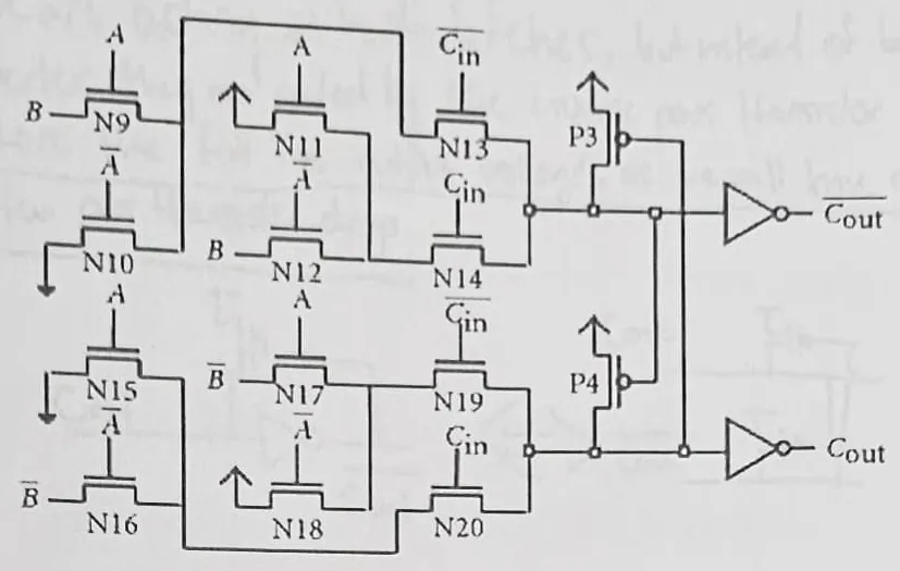
MT24-3, p7 (Fall 2024, 45 points). Consider the pass transistor circuit shown above. (a) Is this a static CMOS circuit? Explain. (10 points) (b) What logic function does this circuit perform to each of the outputs and ? (15 points) (c) What function are transistors P3 and P4 performing? (10 points) (d) Draw a complementary static CMOS circuit implementation that has the same logic function as this pass-transistor circuit. (10 points)
Read the circuit once, node by node, before answering anything (Chapter 10, Section 4). Every internal node is fed by two NFETs whose gates are complements, so each node is a two-way switch: exactly one of its two inputs gets through.
Reading MT24-3 node by node
- P, from N9 and N10. Their gates are A and , so exactly one conducts. N9 passes B and N10 passes ground: for A = 1, P = B; for A = 0, P = 0. So .
- Q, from N11 and N12. Again gates A and . N11 passes and N12 passes B: for A = 1, Q = 1; for A = 0, Q = B. So .
- X, from N13 and N14. Their gates are and , so this pair chooses between the two nodes just found: N13 passes P, N14 passes Q. . X drives the inverter labelled .
- R and S, the lower network. It is the same structure with every data input complemented, so expect complements: N15 (A) passes ground and N16 () passes , so ; N17 (A) passes and N18 () passes , so .
- X̄, from N19 and N20. N19 () passes S and N20 () passes R: , the complement of X in every state. X̄ drives the inverter labelled .
- P3 and P4, the only PFETs. Each runs from to one output node, with the other node on its gate: P3 to X with X̄ on its gate, P4 to X̄ with X on its gate. They are cross-coupled, so whichever node is low turns on the PFET that pulls the other one up.
MT24-3a: is it static?
MT24-3a, p7 (10 points). Is this a static CMOS circuit? Explain.
Hint
What it asks. Whether the circuit is static CMOS, with a reason. The word “static” decides the method: its definition has a half for the settled states and a half for the transitions.
The idea. Static means every node reaches exactly one rail in every settled state, and the right value is reached for any sizing (Chapter 10, Section 9). P3 and P4 are half latches (Chapter 10, Section 6): when a node they hold high must fall, its pull-down meets a PFET that is still on. The tempting answer is “yes, static: only ever one path”, which looks only at the settled states.
Static, or ratioed?
- Settled states first. Without P3 and P4, every internal node is fed through exactly one conducting NFET (the two gates of each pair are complements), and every path ends at a rail or at an inverter that drives B or . In every state each node is connected to exactly one rail: the pass networks alone are static, with weak highs.
- Choose a transition that makes a held node fall. P3 holds X high, so take the inputs from A, B, = 1, 1, 0 (X = 1) to 0, 0, 0 (X = 0). Before: X = 1, held at by P3, because its gate X̄ is 0.
- Look at X just after the change. N10 and N13 now pull X toward ground, but P3 is still on, because its gate X̄ is still 0. X is connected to both rails at once: a fight.
- Ask whether X̄ can free X by itself. N18 and N19 lift X̄, but through NFETs only, so to at most (the threshold rule). P3 turns off only when its gate is within of . With equal thresholds, leaves P3 exactly at its threshold (); body effect (Chapter 5, Section 1) leaves the passed high a little lower still, so P3 stays partly on.
- So the sizes decide the contest. X is pulled down against P3 until it falls past the inverter’s threshold and P4 takes X̄ to ; where X sits meanwhile depends on the sizes. added Model every device as a resistor (Chapter 10’s switch model, a PFET counting ). The pull-down is two 1 µm NFETs in series, ; P3 of width is . X sits on the divider between them: V. That is 1 V for (X switches), 2.5 V for , 4 V for (X still reads as 1).
- Apply the lecture’s test. Correct operation depends on P3 and P4 being weak against the pass paths: by the lecture’s definition (Lecture 10, 50:43), that is ratioed logic.
Check. The divider’s limits behave as they must. As , : with no half latch there is no fight, and the pass network alone is static, as in step 1. As grows, V: a strong P3 always wins. The result swings with one width, so it is ratioed.
Answer: No. In every settled state each node has one path to one rail, but the cross-coupled half latches P3 and P4 make the circuit ratioed: on every transition the falling node must overpower a PFET that is still on, so the circuit works only if P3 and P4 are sized weak.
Remember. “Static?” is two checks: the settled states (one rail per node) and a transition (does anything fight?). A PFET held on by another node, a half latch, passes the first and fails the second. On the exam, write both.
The answer key differs
It says “Yes, this is static CMOS as there is only ever one path from the outputs to VDD/GND”. That is the settled-state view, and it ignores the transitions. The key’s own rubric gives “partial for understanding static criteria, full points for saying not static due to half latches”. Chapter 10 (Section 6) and Chapter 11 (Section 8) side with the rubric. The judgement rests on P3 being left at (or just above) its threshold in step 4.
MT24-3b: the function
MT24-3b, p7 (15 points). What logic function does this circuit perform to each of the outputs and ?
Hint
What it asks. The Boolean function at each of the two labelled outputs. The words “to each of the outputs” decide the last step: after finding what each node computes, you still have to follow it through its inverter to the label.
The idea. A pass network is a tree of two-way switches, so its function is built by composing them: “if the gate is 1, this input, else that one” is (Chapter 10, Section 4). The reading did that node by node. What is left is to simplify, recognize the function, and read the labels.
The function
- Start from the reading. . For that is ; for it is .
- Find one expression for both cases. works: with the second term vanishes, and with it gives , which already contains .
- Recognize it. is 1 when at least two of the three inputs are 1. That is the majority function, the carry-out of a full adder.
- Follow each node to its label, because the inverters sit between the nodes and the labels. X feeds the inverter labelled , so that output is , and X̄ feeds the inverter labelled , so that output is X. Both labels are right.
- Write the truth table, which the question’s 15 points expect (A B → ): 000 → 0, 001 → 0, 010 → 0, 011 → 1, 100 → 0, 101 → 1, 110 → 1, 111 → 1; is the complement in every row.
Check. Trace one row straight through the switches, without the algebra. A, B, = 1, 0, 1: selects Q through N14; A = 1 makes Q = through N11. So X = 1 and , matching row 101. The lower network gives R = 0 (N15 passes ground), so X̄ = 0: the two nodes are complements, as they must be.
Answer: , the carry (majority) of A, B and ; is its complement.
Remember. Compose the switches into terms, simplify, then follow each node through its inverter to its label. Here the upper network computes the carry itself, but its inverter is labelled : reading the node as the output would invert your answer.
The answer key agrees
MT24-3c: what P3 and P4 do
MT24-3c, p8 (10 points). What function are transistors P3 and P4 performing?
Hint
What it asks. The job of the two PFETs. “Function” here means their purpose in the circuit, not a Boolean function: what would be wrong without them, and how they fix it.
The idea. Every high in the pass networks arrives through NFETs, and an NFET passes a 1 only up to one below its gate (the threshold rule, Chapter 10, Section 5). A degraded high costs noise margin, and it leaves the next inverter’s PFET partly on. A half latch fixes it with feedback: a PFET from whose gate is low exactly when its node should be high (Chapter 10, Section 6).
P3 and P4
- Find the level without them. Highs reach X and X̄ only through NFETs (N11 and N18 pass ; N9, N12, N16 and N17 pass B or ), and every one of those NFETs has a full-rail gate. So the high node stops at , one threshold (for A, B, = 1, 1, 0, X = ).
- Find the other node. Lows pass fully through NFETs, because the source stays at 0 V. So in every state the other node is a clean 0.
- See what that clean 0 does. It sits on the gate of the PFET that feeds the high node (P3 for X, P4 for X̄). That PFET turns on and pulls the high node the rest of the way to .
- Name it. This is the lecture’s half latch, with one difference: Lecture 10 wraps the PFET around an inverter on its own node, while here the complementary node already supplies the inverted signal, so the two PFETs are simply cross-coupled.
- Say why it matters. The output inverters see a full , so their PFETs turn fully off and the high noise margin isn’t eaten (Chapter 10, Section 5).
- Give the price. It is part (a): every transition starts with a fight against one of them, so they must be weak.
Check. Trace one row, A, B, = 1, 1, 0, with Chapter 10’s 5 V and 1 V. X: N13 passes P, and N9 passes B = 1 into P, so the pass network leaves X at V. X̄: N19 passes S, and N17 passes into S, so X̄ is a full 0 V. P3’s gate is X̄, so V and P3 is fully on: X goes to 5 V. P4’s gate is now X = 5 V, so P4 is fully off () and leaves X̄ at 0. The settled state is consistent and nothing fights: the fight of (a) happens only on a transition. The widget below (after MT23-2c) shows every row with and without the latches.
Answer: P3 and P4 are cross-coupled half latches. The pass networks give only on the high node; the other node is a full 0, which turns on the PFET feeding the high node and restores it to . They must be weak, because the node that next falls has to overpower them.
Remember. A PFET from whose gate is the complementary node is a half latch: it restores a high that NFETs degraded, and it makes the circuit ratioed. Expect the “static?” part and the “what do they do?” part to be two sides of the same device.
The answer key agrees
MT24-3d: a static CMOS equivalent
MT24-3d, p8 (10 points). Draw a complementary static CMOS circuit implementation that has the same logic function as this pass-transistor circuit.
Hint
What it asks. A complementary static CMOS circuit (a pull-up network of PFETs that is the dual of a pull-down network of NFETs) with the same two outputs as the pass-transistor circuit: and .
The idea. The pull-down conducts when the output should be 0, so a single complementary gate computes the complement of its pull-down’s expression (Chapter 7, Section 4). So build as one gate whose pull-down expresses , draw the pull-up as its dual (series ↔ parallel), and add an inverter for . Factoring the expression first saves transistors, as the lecture’s AOI gates do (Chapter 7, Section 5).
The static CMOS carry
- Choose what the gate computes. , as one gate, then an inverter for ; the circuit then has both outputs, like the original.
- Pull-down, from the expression. It must conduct when . An AND is a series pair and an OR is a parallel pair, so: NFETs A and B in series, in parallel with (A ∥ B) in series with . Five NFETs, stacks two high.
- Pull-up, the dual. Swap every series for parallel and back: PFETs (A ∥ B) in series with (A–B in series, in parallel with ). Five PFETs; the A–B path is three high.
- Count, because the factoring is what saves transistors. 10 transistors in the gate, 12 with the inverter. Writing the majority unfactored, , also works but needs 12 in the gate (14 in all).
Check. Two rows, one for each output value. A = B = 1: the pull-down’s A–B branch conducts and the pull-up’s (A ∥ B) is off, so and . A = B = 0, : no pull-down branch conducts (each needs A or B), while the pull-up’s (A ∥ B) is on and so is its A–B series pair, so and . In both rows exactly one network conducts, as a static gate must.
Answer: the factored majority gate above, followed by an inverter.
Remember. For “draw a static CMOS equivalent”: build the complement of the output as one gate (pull-down = the expression, pull-up = its dual), then invert. Factor the expression first.
The answer key agrees
It draws the same circuit.
2. MT23-2: a pass-transistor full adder
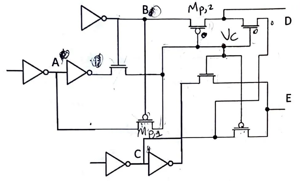
MT23-2, p5–6 (Fall 2023, 34 points). Consider the pass transistor circuit shown above. (a) Is this a static CMOS circuit? Explain. (8 points) (b) What logic function does this circuit perform to each of the outputs D and E? (16 points) (c) What is the lowest logic high and largest logic low values this circuit could produce at outputs D and E and under what static values for the input? (10 points)
This circuit is new in one way: its switches are an NFET and a PFET with their gates tied together, not two NFETs with complementary gates. For a full-rail gate signal, still exactly one of the pair conducts, so each node is again a two-way switch.
Reading MT23-2 node by node
- The drivers first, because every pass path ends at one. Inverters make A and (two in a row), B, and C and (two in a row): all full-rail signals.
- Node . Its pair shares the gate B: an NFET passes , and Mp,1 (a PFET) passes A. A gate of 1 turns on the NFET, a gate of 0 the PFET: for B = 1, ; for B = 0, . So .
- Output D. Its pair shares the gate : an NFET passes C, and Mp,2 (a PFET) passes B. For , D = C; for , D = B.
- Output E. Its pair also shares the gate : an NFET passes , and a PFET passes C. For , E = ; for , E = C.
- Note what drives the gates. is itself a pass-transistor output, and it steers four gates. A degraded would weaken every device it drives. That is what part (c) is about.
MT23-2a: is it static?
MT23-2a, p5 (8 points). Is this a static CMOS circuit? Explain.
Hint
What it asks. The same question as MT24-3a, about a circuit without half latches. As there, “static” needs both checks: one rail per node in every settled state, and the right value for any sizing.
The idea. Same test as MT24-3a; what differs is that nothing here can fight. A fight needs two conducting paths to different rails on one node, and that needs either a half latch (a device held on by another node) or two switches of one pair on at once. With full-rail gates, neither happens. The one thing to check is the one input that is not full-rail: on the gates of the output pairs.
Static?
- One path per node. , D and E are each fed by an NFET and a PFET with the same gate signal. For a gate at a full 0 or 1, exactly one of the two conducts.
- Each path ends at one rail. Every conducting path leads back to an inverter output, which is connected to one rail.
- Nothing fights. There is no half latch and no feedback, so no device has to overpower another. The sizes change the speed, never the logic value: Chapter 10’s test for static.
- Check the one gate signal that isn’t full-rail. is degraded in two states ( or , part c) and drives the D and E pairs. With on its gate, Mp,2 has : with equal thresholds that is exactly its threshold, so it is still off. In the threshold model every node keeps exactly one path in every state (the widget below flags these devices “at the edge”).
Check. Compare with MT24-3a, where the answer was “ratioed”: there P3 stays on because another node holds its gate low while its own node must fall. Here every gate is an input or , and none of them depends on the node it steers, so no node can hold itself.
Answer: Yes, static. In every input state each of , D and E is connected to exactly one rail, through a complementary pair with a common gate, and nothing depends on sizing. It is not complementary static CMOS, and some levels are degraded, but it is neither ratioed nor dynamic.
added If you have time, add the caveat of step 4: the degraded leaves the “off” device of the next pair right at its threshold, so in a real circuit (body effect, or ) it would conduct slightly.
Remember. Static fails through a fight (a half latch, two drivers on a node) or a float (no path). With no feedback and full-rail gates, a pass circuit is static, even when its levels are degraded.
The answer key agrees
MT23-2b: the functions
MT23-2b, p5 (16 points). What logic function does this circuit perform to each of the outputs D and E?
Hint
What it asks. The Boolean functions at D and E, in terms of A, B and C. The 16 points go to an expression and a truth table for each.
The idea. Same method as MT24-3b: compose the two-way switches of the reading, then simplify. The new step is a substitution: when , D passes B, and means A = B, so B can be read as A or as B, whichever makes the expression recognizable.
D and E
- The steering signal. (reading, step 2): it is 1 exactly when A and B differ.
- D, case by case. If A ≠ B (), D = C. If A = B (), D = B, and since A = B there, that is also . So .
- Recognize D. Expand: . D is 1 when at least two inputs are 1: the majority, a full adder’s carry.
- E, case by case. gives and gives C, which is “C inverted when is 1”: , a full adder’s sum.
- Write the truth table, which the question’s 16 points expect for each output (A B C → D E): 000 → 0 0, 001 → 0 1, 010 → 0 1, 011 → 1 0, 100 → 0 1, 101 → 1 0, 110 → 1 0, 111 → 1 1.
Check. A full adder adds three bits, so D and E together must count the ones in each row as the binary number DE. Row 011: two ones, DE = 10 ✓. Row 111: three ones, DE = 11 ✓. Row 100: one, DE = 01 ✓.
Answer: (the carry) and (the sum): the circuit is a full adder.
Remember. A switch steered by is the sign of an adder: the carry passes C when A and B differ and A (= B) when they agree; the sum is C, inverted when A and B differ.
The answer key agrees
It writes , the same function.
MT23-2c: the worst levels
MT23-2c, p6 (10 points). What is the lowest logic high and largest logic low values this circuit could produce at outputs D and E and under what static values for the input?
Hint
What it asks. The lowest voltage that D or E can have while it is a logic 1, the highest while it is a logic 0, and the input states that produce them. “Under what static values for the input” means you must name a row that really gives the level.
The idea. Apply the threshold rule (Chapter 10, Section 5) along each path. An NFET passes a 1 only up to one below its own gate, and a PFET passes a 0 only down to one above its gate. So a level loses one threshold when a 1 goes through an NFET (or a 0 through a PFET) with a full-rail gate, and a second one only when that device’s gate is itself degraded. The tempting slip is to count devices in series: a 1 that crosses two NFETs with full gates loses one threshold, not two. Here the degraded gate is , so first find when is degraded, then which output passes a 1 (or a 0) through a device that steers.
Worst high and worst low
- When is degraded? A = 0, B = 1: the NFET (gate B) passes , so . A = 0, B = 0: Mp,1 passes A = 0, so . In the other two states is a full rail, because each device then passes the value it passes well (the NFET a 0, the PFET a 1).
- Lowest high. We need a 1 that passes through an NFET whose gate is : it stops one below that gate, at . is high, so the NFETs conduct: D = C, E = . At D this gives a 1 for A, B, C = 0, 1, 1; at E for 0, 1, 0. The figure below marks the path for D.
- Highest low. The mirror: a 0 that passes through a PFET whose gate is stops one above that gate, at . is low, so the PFETs conduct: D = B, E = C. D is 0 for A = B = 0 with C either (through Mp,2); E for 0, 0, 0 (through E’s PFET).
- Single drops elsewhere, for comparison. A, B = 1, 0 makes , so D (for C = 1) and E (for C = 0) reach through their NFETs; A, B = 1, 1 makes , so E (for C = 0) only falls to .
- Put in numbers. With Chapter 10’s and : the worst high is 3 V and the worst low is 2 V. The two outputs can be only 1 V apart.
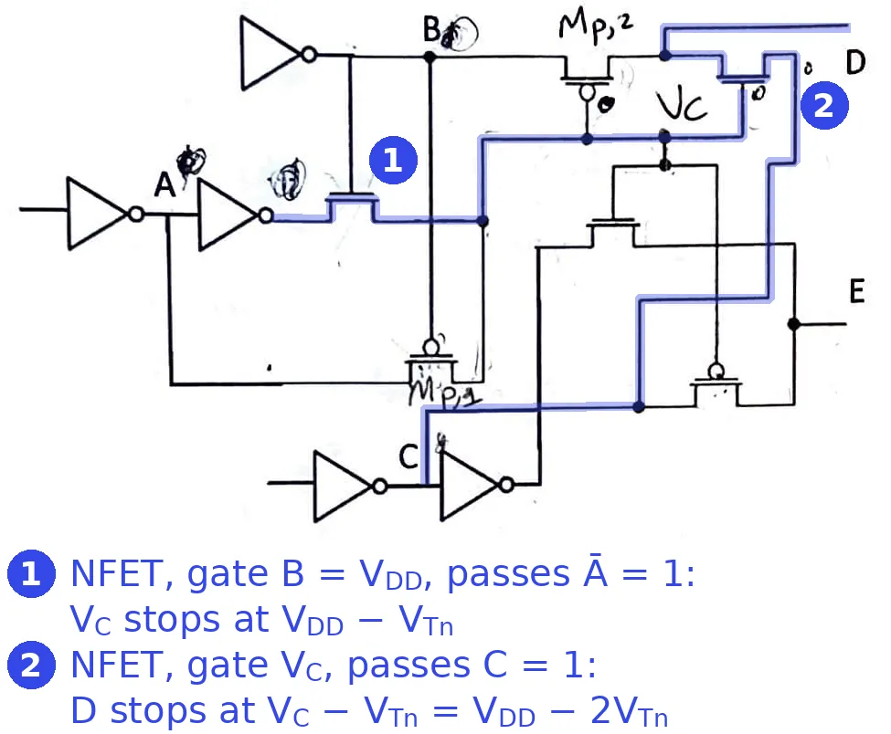
Check. Every worst row has A = 0, and that is no accident. ’s NFET passes , which is a 1 (the value an NFET degrades) only when A = 0; its PFET passes A, which is a 0 (the value a PFET degrades) also only when A = 0. With A = 1, is a full rail and no output can lose more than one threshold. The widget below shows every row.
Answer: Lowest high : at D for A, B, C = 0, 1, 1 and at E for 0, 1, 0. Highest low : at D for 0, 0, 0 and 0, 0, 1, and at E for 0, 0, 0. Both come from the degraded driving the gate of the next pass device (Chapter 10, Section 5, its last check).
Remember. One threshold per path, plus one more where a degraded node drives a gate. To find the worst row, first find when the steering node is degraded, then pick the output value that passes through the device it steers.
The answer key differs
It gives the lowest high for “A = 1, B = 1, C = 1”. It doesn’t occur there: passes through the NFET as a strong 0, so , Mp,2 is on and passes B = 1 to D at the full . The worst high needs A = 0, B = 1, so that is the degraded . The key’s levels themselves, and its low example (A = B = 0), are right.
Run both adders here. Every node shows its logic value and its level; the table runs all eight rows.
What to notice.
- MT23-2, A, B, C = 0, 1, 1: is and D is ; Mp,2 and the PFET of E are flagged at the edge of conduction. Now set A = 1: becomes a full 0 and D a full (the key’s example).
- MT24-3 without P3 and P4: every high node is , never worse, because every NFET’s gate is a full-rail input. With them, every high node is restored to .
- The widget shows settled states only. The fight that makes MT24-3 ratioed happens during a transition (MT24-3a); the switch-level widget of Chapter 10, Section 4 replays transitions for the lecture’s circuits.
Check yourself MT24-3's pass networks lose at most one threshold, while MT23-2's lose two. What is the structural difference?
In MT24-3 every pass NFET’s gate is a full-rail input (, , , ), and series NFETs with full gates lose only one in total. In MT23-2 the gates of the output pairs are driven by , which is itself a pass-transistor output and can be degraded; a device whose gate is one threshold short stops one threshold below that, two in all.
3. MT21-1: a pass-transistor multiplexer
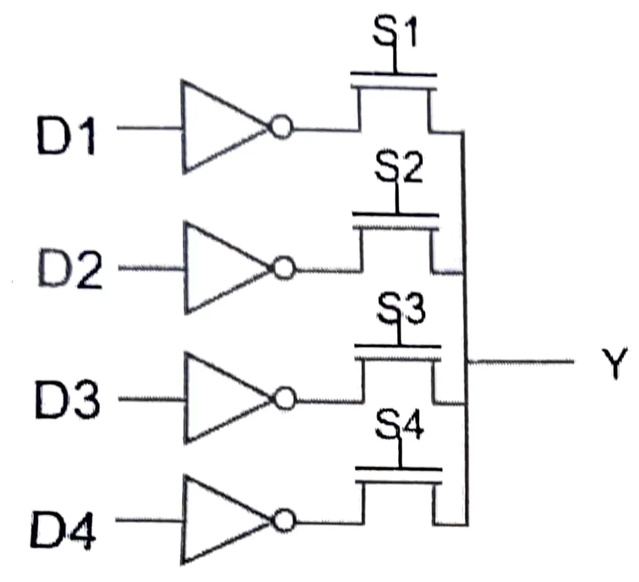
MT21-1, p2–3 (Fall 2021, 30 points). Consider the pass transistor multiplexer shown above. (a) What logic constraint on S1, S2, S3, and S4 ensures that this is a static CMOS circuit? (10 points) (b) In normal operation, what output high voltage will be achieved relative to the supply voltage ? Explain. (10 points) (c) Draw a complementary static CMOS circuit that achieves the same logic functionality of the pass transistor design. (10 points)
MT21-1a: the constraint on the selects
Hint
What it asks. A rule on the four selects under which the multiplexer is static. Here the circuit is static or not depending on the inputs, so the answer is a condition, not a yes or no.
The idea. Static means exactly one path from Y to one rail (Chapter 7, Section 4). Unlike MT24-3 and MT23-2, these selects are four independent signals, not complements, so the circuit itself no longer guarantees one path: the selects must. Count Y’s paths for each number of selects that are on (Chapter 10, Section 7).
When is the multiplexer static?
- List the paths. Y has four possible paths, one per NFET, each to an inverter output and through it to one rail.
- No select on. Y is connected to nothing and floats. That is dynamic, not static.
- Two selects on, with different data. One inverter pulls Y up while another pulls it down, a fight decided by strength: ratioed.
- Exactly one select on. Exactly one path, to exactly one rail. Static.
Check. The condition must exclude both failures, and “exactly one” does: “at most one” still allows the float, and “at least one” still allows the fight. A decoder’s outputs satisfy it by construction, which is why the lecture drives the selects from one.
Answer: exactly one of S1–S4 must be 1 at any time (the selects are one-hot, for example from a decoder).
Remember. When the gate signals are independent, being static is a condition on the inputs: no fight (at most one path) and no float (at least one). For a multiplexer, that is one-hot selects.
The answer key differs
It says “only one of the inputs can be logic 1 at any given time”, which reads as at most one. All four at 0 is also not static (Y floats), so say exactly one.
MT21-1b: the output high
Hint
What it asks. The voltage Y reaches when the multiplexer outputs a 1, relative to , with the reason. “In normal operation” means one-hot selects: a single NFET with its gate at connects Y to one inverter.
The idea. This is the threshold rule itself, the single-drop case of MT23-2c (Chapter 10, Section 5). An NFET’s source is whichever of its two terminals is lower. Passing a 1, that is the output, so the output’s own rise eats into until the device cuts off. The gate is a full-rail select, so there is no second drop.
The high level
- Set up a 1 on the path. Say S3 = 1 and D3 = 0: the third inverter’s output is , and the third NFET has its gate at .
- Find the source. Passing a 1, the NFET’s lower terminal is Y, so Y is its source and .
- Follow Y up. As Y charges, shrinks; the NFET cuts off when , at .
- Add what the model leaves out. Body effect raises as the source rises, so a real NFET stops a little lower still.
- Put in numbers, for example. The exam gives no values, so the answer stays symbolic. With illustrative values, and (Chapter 10’s exam-style check; not the exam’s numbers, and not this page’s 5 V / 1 V), it is 2.0 V.
Check. The low side, by the same reasoning: passing a 0, the source is the inverter’s side, at 0 V, so stays at the whole way and Y reaches ground. An NFET-only multiplexer is asymmetric, a full 0 and a weak 1, which is what the rule predicts.
Answer: , because the pass NFET turns itself off once its gate is only above the output.
Remember. An NFET passing a 1 stops one below its gate, because the output is its source. One drop, however many NFETs with full gates are in series.
The answer key agrees
Its answer is the same, but it writes (“high ”). At cut-off it is ; it is the output that sits at .
MT21-1c: a static CMOS equivalent
Hint
What it asks. A complementary static CMOS circuit with the same function as the multiplexer, inverters included. Only the function has to match, not the structure.
The idea. Same move as MT24-3d: a single complementary gate computes the complement of its pull-down’s expression (Chapter 7, Section 4). What is new is that the multiplexer already inverts (it passes ), so with one-hot selects Y is itself the complement of an AND-OR expression, and one AND-OR-invert gate does it with no inverter at all (Chapter 7, Section 5).
An AND-OR-invert gate
- Write the function. With the inverters, the multiplexer passes : , assuming one-hot selects.
- Rewrite it as a complement, because that is what one gate computes. With one-hot selects, if is the select that is on, : only the -th term can be 1.
- Draw the gate. That is an AND-OR-invert gate: the pull-down has four series pairs (, ) in parallel; the pull-up, its dual, has four parallel pairs ( ∥ ) in series. 16 transistors, and no inverters: goes straight in.
- Note its cost. Its PFET stack is four high, which Chapter 7 would avoid in practice. The question asks only for a circuit with the same function.
- Compare the key’s form. It uses the complements instead: pull-down in series with the other three such pairs, pull-up four series branches (, ) in parallel. It computes exactly, for any selects, but needs four inverters for , and its NFET stack is four high.
Check. One row each way. S3 = 1, D3 = 0: in the pull-down the S3–D3 pair is off, and every other pair has its select off, so the pull-down is off; in the pull-up, pairs 1, 2 and 4 conduct through their select PFETs (selects at 0) and pair 3 through its PFET, so Y = 1 = ✓. With D3 = 1 the S3–D3 pair conducts and Y = 0 ✓.
Answer: the AOI gate above (or the key’s equivalent form with ).
Remember. A pass-transistor multiplexer with one-hot selects is an AND-OR(-invert) of selects and data. Write the function as a complement first, then draw one gate.
The answer key agrees
It writes : the third term should be . Its circuit is otherwise correct.
4. MT21-3: the six-transistor XOR
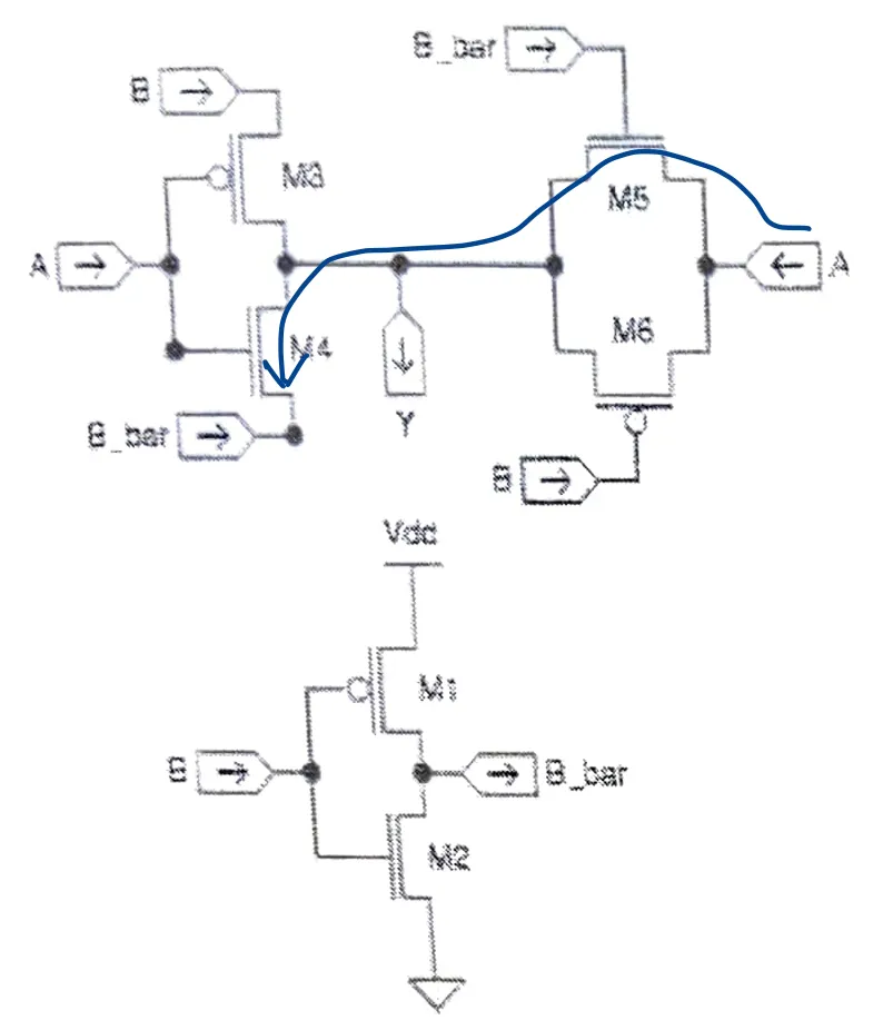
MT21-3, p5 (Fall 2021, 25 points). Consider the six-transistor XOR gate shown above. As discussed in class, this is not a static CMOS circuit. Describe how one could size the circuit such that it produces a logically incorrect result.
Hint
What it asks. A sizing that makes the gate give a wrong answer. The question already tells you the gate is not static, so the job is to find the transition where two paths fight, and say which device must lose for the wrong side to win.
The idea. Why the 6T XOR is ratioed (Chapter 10, Section 9): a settled-state check passes, because each row of the truth table has one path from Y to one rail. But on one transition a node is pulled both ways, and that node, , is also the gate of a pass device (M5). So whichever side wins the fight decides whether M5 turns off, and with it the final state. A fight whose winner decides the answer is what makes a gate ratioed; a brief overlap that always ends the same way does not. Include the gates that drive A and B, as the lecture does (Lecture 10, 46:05): the fight runs through A’s driver.
The failing transition
- Name the devices. M1 and M2 make from B; M3 (PFET, gate A) joins B to Y; M4 (NFET, gate A) joins to Y; M5 (NFET, gate ) and M6 (PFET, gate B) join A to Y. Every row of the truth table gives XOR.
- Add the drivers, because the fight’s path runs through one: every node is driven by a real gate.
- Start at A = 1, B = 0. , so M5 and M6 pass A = 1 to Y; M4 (gate A = 1) also joins Y to , which is 1 too. Y = 1, and nothing fights.
- Switch B to 1, and say what should happen. Y should fall: M2 pulls down, M5 turns off, and M4 pulls Y down to .
- Find the path that resists. While is still high there is a path from through the PFET of A’s driver, M5 (gate , still on), Y and M4 (gate A = 1) to . It holds up against M2.
- Choose the sizes that let it win. Size M2 very weak, and M5, M4 and A’s driver strong. Then never falls far enough, M5 stays on, and Y stays at 1 for A = B = 1: the wrong answer, with current flowing from to ground.
- Put numbers on it added. With every device as (A’s driver PFET 2 µm, M5 and M4 1 µm, so the path is per µm), sits on a divider between that path and M2’s : for an M2 of width in µm. gives 1.25 V (it switches); gives 3.125 V, with Y at 3.75 V (it fails). The switch-over is at .
Check. At the switch-over, , M2’s resistance is , equal to the path’s , and , half the supply. A ratioed contest should flip exactly where the two sides are equally strong, and it does.
Answer: make M2, the NFET of the inverter that produces , much weaker than the series path through A’s driver, M5 and M4. Then on the transition A = 1, B: 0 → 1, can’t be pulled low, M5 stays on and Y stays at 1. Because correct operation depends on sizing, the gate is ratioed.
Remember. To show a gate is ratioed, give a transition, the two paths that fight on one node, and the device whose weakness lets the wrong side win. The truth table alone can never show it.
The answer key agrees
It names the M5–M4 path; the PFET of A’s driver belongs to that path too.
Check yourself Does the 6T XOR fail on any other transition? Consider A = 0, B: 0 → 1.
It fights only briefly. When B rises, falls on its own (M2 pulls it down and nothing holds it up, since M4 is off with A = 0). M5 turns off, M3 connects Y to B = 1, and the gate settles correctly whatever the sizes. A transient overlap is not what makes a gate ratioed; a fight whose winner decides the final state is. Only 10 → 11 has one (Chapter 10, Section 9).
How to approach a stick-layout question
Recognize it by the picture: two rails ( at the top, ground at the bottom), two horizontal diffusion lines (p near , n near ground), vertical poly lines labelled with the inputs, metal lines, and square contacts. The question always says “Draw the schematic corresponding to this layout. What logic function does this gate perform?” It is short: 15 of 200 points in 2024 and 10 of 150 in 2023, about five minutes, with most of the points for the schematic.
The moves, in order.
- Find the transistors. Every place a poly line crosses a diffusion line is one transistor, with that poly’s signal on its gate: a PFET on the p line, an NFET on the n line.
- Name the nodes. The pieces of diffusion between polys are the transistors’ sources and drains. A contact joins a piece to the metal over it; follow that metal to name the net (, ground, the output, or an internal net). A poly with no input label gets its signal through a contact from metal, so it is driven by an internal net.
- Series or parallel. An uncontacted piece joins only its two neighbours, so they are in series. Two transistors whose ends reach the same two nets are in parallel, wherever they sit on the line.
- Find the stages. A net that ends on a poly is a gate’s output driving another gate: the layout has two stages.
- Then the function. Write each stage’s pull-down, check that its pull-up is the dual, and compose the stages.
Why these rules (Chapter 9, Section 10). A stick diagram draws one line per layer, so a transistor is exactly where gate poly crosses active diffusion, and only a contact joins two layers: metal that merely crosses a poly or a diffusion line touches nothing. Neighbouring transistors on one line share the diffusion between them (Chapter 5, Section 6): uncontacted, that shared piece is an internal node of a series stack; contacted, it is a net that other devices may also reach. The duality check comes from complementary static CMOS (Chapter 7, Section 4): if your pull-up is not the dual of your pull-down, you have misread a contact.
Traps. Metal crossing a poly or a diffusion line without a contact (both exam figures have one). A poly with no input label, which means a second stage (without MT24-4’s inverter you would answer NOR, not OR). Calling two transistors in series because they sit side by side, when their outer ends reach the same nets.
5. MT24-4: a stick layout with two stages
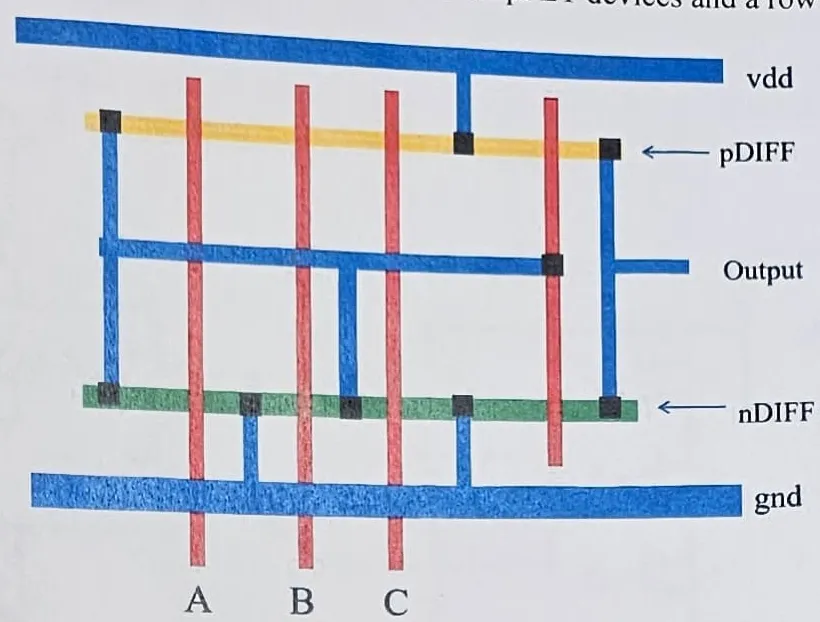
MT24-4, p9 (Fall 2024, 15 points). Consider the stick layout above with a row of pFET devices and a row of nFET devices. Draw the schematic corresponding to this layout? What logic function does this gate perform? (Schematic 10 points, output 5 points.)
Hint
What it asks. The schematic of the eight transistors (10 points) and the logic function at “Output” (5 points). The unlabelled fourth poly is the detail that decides the function.
The idea. Read it with the rules of the section above (Chapter 9, Section 10): transistors where poly crosses diffusion, nets named by following contacts and metal, series through uncontacted pieces, parallel where two devices reach the same two nets. The new idea here is a second stage: one metal net both collects the first gate’s output and ends in a contact on the fourth poly, so the first gate drives the second.
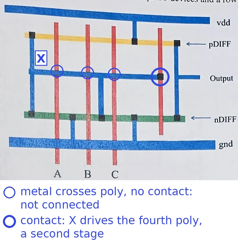
Reading the layout (Chapter 9's rules)
- Count the transistors. Four poly lines cross both diffusion lines: eight transistors. A, B and C enter from the bottom; the fourth poly has no input label and gets its signal through the contact on it.
- Name the metal, because the nets decide every connection. The left vertical line joins the left ends of both rows and runs along the horizontal line to the contact on the fourth poly: call it X. The right vertical line joins the right ends of both rows: the output. The horizontal line crosses polys A, B and C with no contact, so it does not touch them.
- PFET row, left to right: X, poly A, an uncontacted piece, poly B, an uncontacted piece, poly C, a contact to , the fourth poly, the output. The uncontacted pieces join only their neighbours, so A, B and C are in series from to X (C nearest ), and the fourth PFET runs from to the output.
- NFET row: X, poly A, ground, poly B, X (the contact wired up to the horizontal line), poly C, ground, the fourth poly, the output. A runs from X to ground, B from ground to X, C from X to ground: every one reaches the same two nets, so all three are in parallel between X and ground (Chapter 5, Section 6). The fourth NFET runs from ground to the output.
- Find the stages. First stage: series PFETs over parallel NFETs, , a three-input NOR. Second stage: one PFET and one NFET, both gated by X, between the rails and the output: an inverter.
- Compose them. .
Check. Duality: the first stage’s pull-up (A, B, C in series) is the dual of its pull-down (A, B, C in parallel), as a complementary gate’s must be. And every transistor is used once: six in the NOR, two in the inverter, eight in all, matching the eight crossings.
Answer: a three-input NOR whose output X drives an inverter: , an OR gate.
Remember. A poly with no input label is driven by an internal net, so look for a second stage before you write the function. Chapter 9’s exam-style practice is the two-input version of this layout.
The answer key agrees
6. MT23-4: a stick layout with four inputs
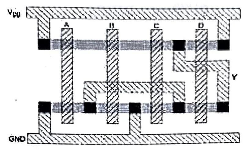
MT23-4, p10 (Fall 2023, 10 points). Consider the stick layout above with a row of pFET devices and a row of nFET devices. Draw the schematic corresponding to this layout? What logic function does this gate perform?
Hint
What it asks. The schematic and the logic function of a single gate with four inputs. Every poly is labelled, so there is one stage; the work is in the nets.
The idea. Same rules as MT24-4. What is different: one stage, and an internal net (P) that is contacted and joined by metal, so devices that are not neighbours on the line still meet at it. That is how a parallel group and a series device share one row.
Reading the layout
- Count the transistors. Four polys, A to D, each cross both rows: eight transistors.
- PFET row: , A, an uncontacted piece, B, an uncontacted piece, C, a contact wired to Y, D, . The uncontacted pieces make A, B and C in series from to Y; D runs from Y to , the same two nets, so it is in parallel with that stack.
- NFET row: ground, A, a contact (call its net P), B, ground, C, a contact wired to the first one by the metal line (P again), D, Y. A runs from ground to P, B from P to ground, C from ground to P: all reach the same two nets, so they are in parallel between ground and P. D runs from P to Y.
- Write both networks. Pull-down: D in series with (A ∥ B ∥ C); it conducts when . Pull-up: (A–B–C in series) ∥ D, which is its dual, as it must be.
- The function. The output is low when the pull-down conducts: , an OR-AND-invert gate.
Two traps in this figure. The Y metal crosses poly D on its way down, and the P metal crosses polys B and C; neither has a contact there, so neither connects.
Check. One row through the transistors themselves. A = B = C = 0, D = 1: on the n line the D NFET is on but A, B and C are all off, so P has no path to ground and the pull-down is off; on the p line A, B and C are all on, so the series stack pulls Y to . Y = 1, and the formula gives ✓.
Answer: .
Remember. Name every contacted piece by its net before deciding series or parallel: devices far apart on a line are in parallel if they reach the same two nets.
The answer key agrees
Check yourself Is the order A, B, C, D in MT23-4 an Euler path of both networks? How can you tell from the layout alone?
Yes. Both diffusion rows run unbroken from end to end, with every pair of neighbouring transistors sharing a piece of diffusion. That is exactly what an Euler path common to both networks buys (Chapter 10, Section 1): straight polys and no breaks in either row.
Patterns
Pass-transistor circuits (every midterm since 2021: 23–37% of the points).
- Moves (the approach): read node by node; static (settled states, then a transition); the function; the levels by the threshold rule; what the half latch restores; one complementary gate plus an inverter.
- The answers that keep coming back: one-hot selects; ; and when a pass output drives a gate; half latches restore the rail but make the circuit ratioed; the carry and the sum .
- Traps: “static” from settled states only; one threshold per series device; a worst-level example that gives a full level; an output label that is the complement of its node; “only one select” for exactly one.
- Time: 15–17 minutes for the whole question (about 30 seconds a point on a 150-point exam, 22.5 on a 200-point one).
Stick layout to schematic (MT23-4, MT24-4: 7–8% of the points).
- Moves (the approach): a transistor at every poly–diffusion crossing; name the nets by contacts and metal; series through uncontacted pieces, parallel to the same two nets; find the stages; then the function, with the duality check.
- Traps: metal crossing without a contact; an unlabelled poly, which means a second stage (NOR, not OR, if you miss MT24-4’s inverter).
- Time: about 5 minutes.
What the keys get wrong
Re-solving every part found these disagreements; all are recorded in this page’s review/decisions.md.
| Part | The key | Here |
|---|---|---|
| MT24-3a | “Yes, this is static CMOS” | Not static: ratioed because of the half latches (the key’s own rubric gives full points for this) |
| MT23-2c | lowest high “Ex: A = 1, B = 1, C = 1” | at 1, 1, 1 D is a full ; the lowest high is at 0, 1, 1 (D) and 0, 1, 0 (E) |
| MT21-1a | “Only one of the inputs can be logic 1” | exactly one: with none on, Y floats |
| MT21-1b | at cut-off ; the output is (the key’s answer is right) | |
| MT21-1c | third term | ; the circuit is otherwise right |
Every other part (MT24-3b–d, MT24-4, MT23-2a–b, MT23-4, MT21-3) agrees with its key after re-solving.