19. SRAM: the 6T cell, its read and write circuits and the decoder
An SRAM is the memory a processor reaches every cycle: its level-one caches and register files. Chapter 18 showed the array: word lines across, bit-line pairs down, a cell at every crossing, a row decoder at the side and the read and write circuits at the bottom. This chapter opens the cell and builds the circuits around it. The cell is the 6T cell, Chapter 13’s loop of two inverters with two access transistors that connect it to the bitlines. It must be small, because the whole array multiplies it, and two requirements pull its three device sizes in opposite directions: a read must not upset it, and a write must succeed. The lecture then builds the column’s periphery on two clock phases: precharge, a word line qualified by the clock, a single-ended read, the write drivers, the column multiplexer and the sense amplifier. It ends with the decoder that raises one word line, built as a dynamic gate pair with a deliberate race. The cell is introduced at the end of Lecture 17 (58:00–64:30) and repeated at the start of Lecture 18; this chapter takes both.
After this chapter you can:
- draw the 6T cell and give its read and write sequences;
- say which devices fight during a write and during a read, and derive the two sizing ratios;
- estimate the node voltage in each fight with a resistor divider;
- read hold, read and write on the butterfly diagram, and say what the largest square measures;
- explain why tiny cell devices fail at random, and name the remedies;
- trace a column’s read and write through the two clock phases;
- size the write path’s stack and say why fewer series devices help;
- draw a column multiplexer, say what it buys and what it costs the write path;
- explain how a clocked sense amplifier reads a small swing, and what its offset costs;
- build a decoder from ANDs, predecode it as NAND–NOR, and qualify it with the clock;
- explain the race in the race-based NOR and state the non-overlap condition;
- estimate a decode path’s and a bitline’s delay, and the access time in FO4.
Boxes and equations marked board were written in the lecture. Parts marked added are explanations or examples this guide adds. The example cell added, used for numbers throughout: a cell PFET of 0.2 µm, access NFETs of 0.3 µm and pull-down NFETs of 0.6 µm (the board’s ratios), a bitline of 120 fF and V. These are this guide’s numbers, not the course’s; each use says “for example”.
Symbols
| Symbol | Meaning | Unit | First appears |
|---|---|---|---|
| bit, | a column’s pair of bitlines (board; FN17 writes B, ) | — | §1 |
| WL | a word line (board “wordline”) | — | §1 |
| , | the cell’s two inner nodes, on the bit side and the side (L17 board) | V | §1 |
| the supply | V | §1 | |
| , , | widths of the cell’s PFET, access NFET and pull-down NFET added | µm | §1 |
| the resistance of a 1 µm NFET pulling down (Chapter 7’s constant of proportionality); a device of width is | kΩ·µm | §2 | |
| the written node’s voltage during a write fight (Chapter 13) | V | §2 | |
| an inverter’s switching threshold (Chapter 6) | V | §2 | |
| the cell ratio added | — | §3 | |
| the voltage the 0 node rises to during a read added | V | §3 | |
| , | the lifted low and the capped high in the butterfly sketches added | V | §4 |
| SNM | static noise margin: the side of the largest square in a lobe of the butterfly added | V | §4 |
| , ; , | the two clock phases and their complements (board) | — | §6 |
| non-overlap time, from falling to rising (Chapter 14) | ps | §6 | |
| , | a bitline’s and a word line’s capacitance added | fF | §7 |
| gate capacitance per µm of width, 2 fF/µm in the examples | fF/µm | §7 | |
| the fan-out-of-one delay (Chapter 7; FN10 writes ) | ps | §7 | |
| the equivalent width of devices in series, | µm | §7 | |
| the bitline’s delay from to added | §7 | ||
| the bitline swing when the read is detected added | V | §7 | |
| data, write | the column’s write data and write enable (board) | — | §8 |
| col 1, col 2 | the column-select lines of a multiplexer (board) | — | §9 |
| , , , | rows, columns, bits per word and words of a memory (Chapter 18’s names; this and are counts) | — | §9 |
| , | the sense amplifier’s two sense nodes added | — | §10 |
| a sense amplifier’s input offset voltage (board “input offset voltage”) | mV | §10 | |
| address bits (board) | — | §11 | |
| , | the race-based NOR’s first- and second-stage nodes added | — | §12 |
| a dynamic stage’s evaluation delay | §12 | ||
| FO4 | the fan-out-of-four delay; FN10 takes FO4 ≈ 3 | §13 |
1. The 6T cell: storing a bit, reading and writing it
You need
Static storage (Chapter 13 §4–§5). Two inverters in a ring hold each other’s outputs: if is high, the inverter it drives makes low, and that inverter’s partner makes high again. The ring has two stable states, and , and keeps either as long as the supply is on. On the butterfly diagram the two transfer curves, one mirrored, cross three times: the two outer crossings are the stable states and the middle one is metastable.
The array (Chapter 18 §10). One row per word line, one column per pair of bitlines. The row decoder raises one word line; the columns end in the read and write circuits.
The question. How do you store one bit in as few transistors as possible, and still read it and write it through wires shared with every other cell in its column?
Six transistors
Building the cell (board, L17 59:32–60:24 and 64:30; L18 01:33)
- Start from the loop. Two inverters, each driving the other’s input, store the bit (Chapter 13). Name the nodes as the board does: on the left, on the right.
- Add two doors. An NFET connects to a vertical wire, bit, and a second NFET connects to its own wire, . Their gates sit on a horizontal wire, the word line. These two NFETs are the access transistors (board, L17 64:30): with the word line low they are off and the loop is sealed; with it high, both nodes are connected to their bitlines.
- Count. Each inverter is a PFET and an NFET, so the cell is transistors. Every cell in a column shares the same bit and ; every cell in a row shares the same word line.
- Symmetric halves. “These two inverters are sized identically. … completely symmetric” (L17 60:24). The left half and the right half are mirror images. §2 and §3 will size the three devices within one half against each other; that does not break the symmetry between the halves.
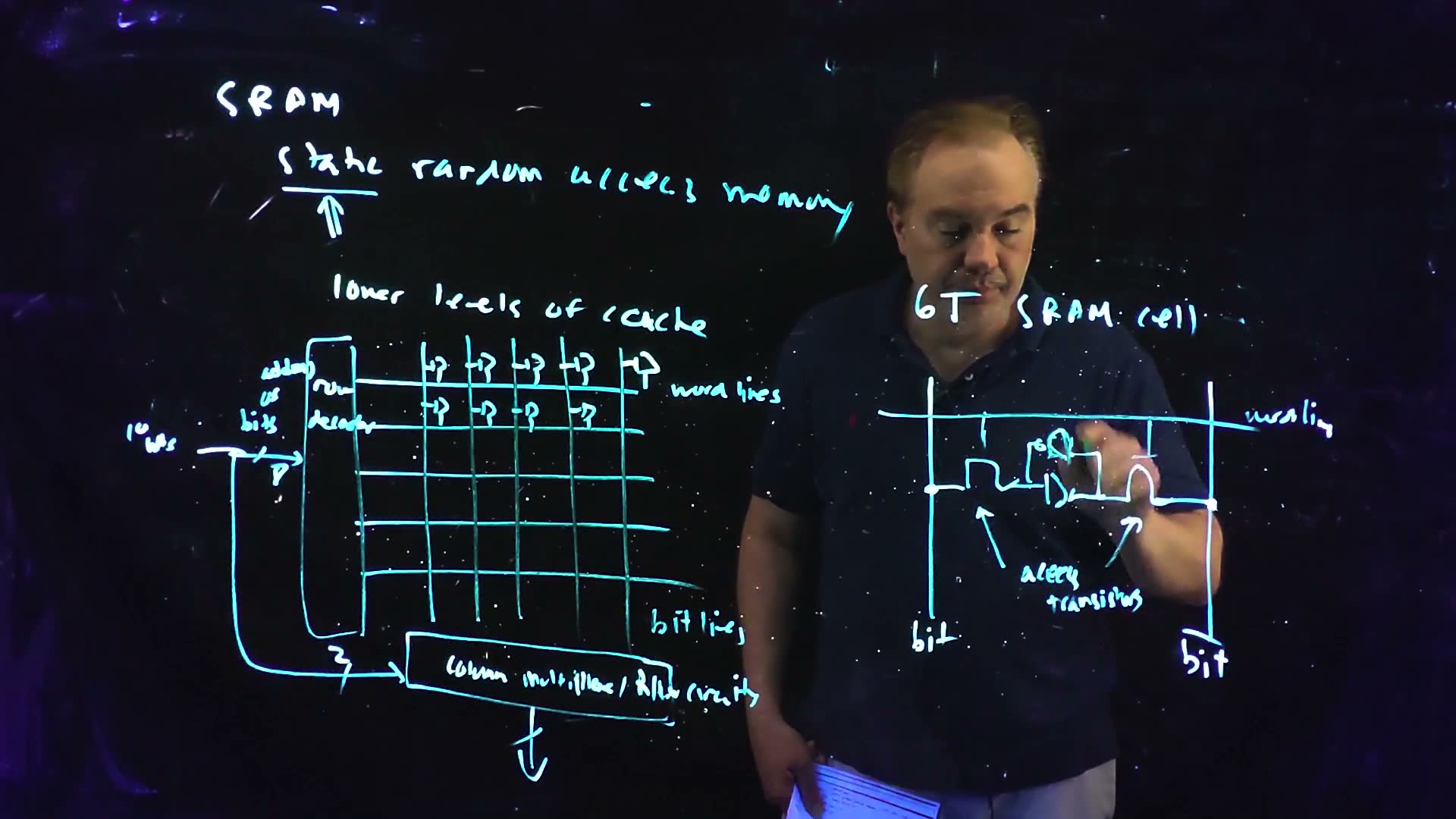
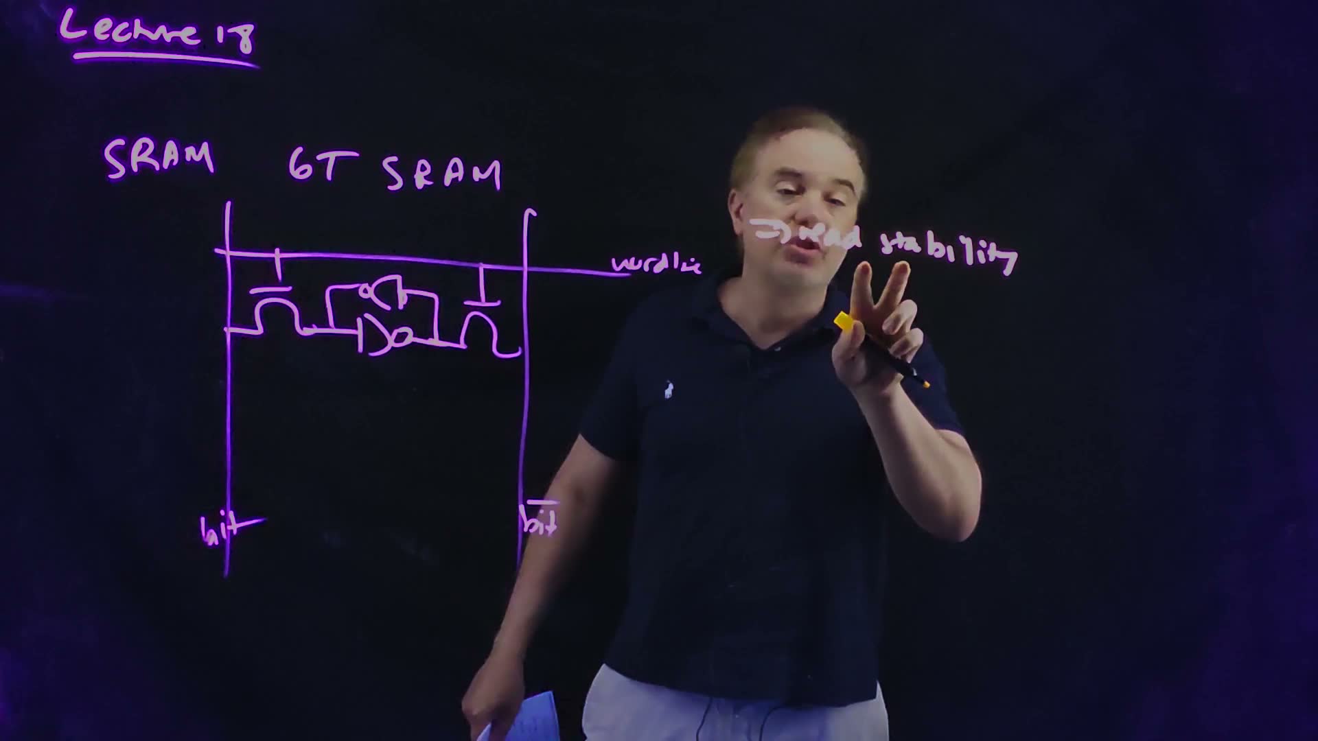
The 6T cell, redrawn from the boards (Lecture17 @ 64:30, Lecture18 @ 01:33). (a) As the boards draw it: bit on the left and on the right, the word line WL across the top, the two access NFETs (gates on WL) from the bitlines to the inner nodes and , and two cross-coupled inverters between the nodes. (b) The same cell with each inverter drawn as its PFET over its NFET: six transistors. One device of each kind is labelled with its width: (the cell’s PFET), (the pull-down NFET) and (the access NFET); the other half is the mirror image.
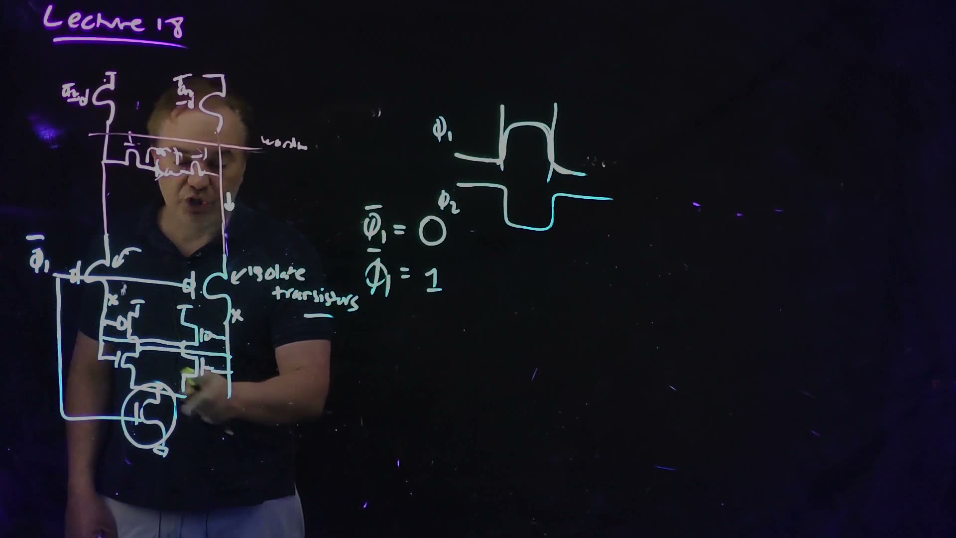
The board (Lecture17 @ 64:30)
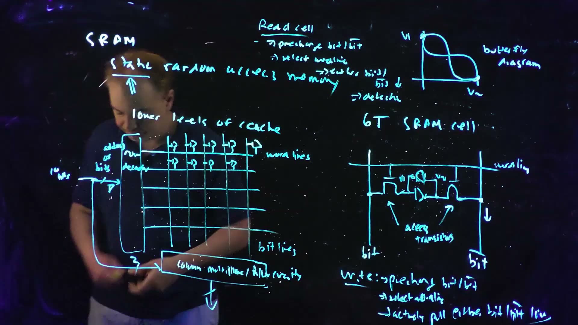
Fair copy of the board above (Lecture17 @ 64:30), mark for mark in its own layout. All black: one cyan pen wrote the whole board. The board draws each transistor as a gate bar over a channel bump and each inverter as a small D shape with a bubble. “address bits” is written in three pieces beside the decoder. The lower-left corner (the bus marked 2 with its slash, and the left end of the column-multiplexer box), under the lecturer’s hands here, is read on 60:47; the array is unchanged since then. “⇒ either bit/”, which the hand squeezed in against “memory”, is set a little to its right.
Reading and writing
The board at L17 64:30 writes both sequences board. Follow a cell that holds , .
A read, then a write (board, L17 64:30; speech 61:25–63:56)
- Read: precharge. Before the access, both bitlines are pulled up to and left there.
- Read: select. The decoder raises the cell’s word line, which turns both access transistors on.
- Read: one bitline falls. On the side, meets a bitline that is also high: no voltage across the access device, no current. On the bit side, is held at ground by its pull-down NFET, so current flows from bit through the access NFET and the pull-down into ground, and bit sags. “One of these will pull down. Not both of them” (L17 62:06). The cell is tiny and the bitline is long, so the sag is slow.
- Read: detect. A circuit at the bottom of the column sees which bitline fell (§7, §10). Bit fell, so .
- Write: precharge and select, as for a read.
- Write: pull one bitline low. To write , a driver at the bottom pulls actively to ground; bit is “kept at its precharge value” (L17 63:31). The low drags down through its access device. Once falls far enough, the inverter it drives raises , and the loop flips. Had the cell already held , the same write would store the same value again.
The read and the write as waveforms added (the sequences are the board’s, Lecture17 @ 64:30; a sketch without values). The cell starts with , . Left, a read: WL rises; bit sags slowly by a small amount while stays high; bumps up a little and stays low; WL falls. Right, a write of : WL rises, and on the same clock edge (§8) is driven quickly to 0; falls and rises until they cross; bit stays high; WL falls and the cell holds the new state.
Why only six, and the two requirements
“Density, of course, is paramount” (L17 59:02). An array has millions of cells, so one more transistor per cell costs millions of transistors. Cells with eight or ten transistors exist, but they have not caught on (L18 17:25; §5). The cell stays at six, and “people have figured out ways of using the peripheral circuits to compensate” (L17 59:32): that is the rest of this chapter.
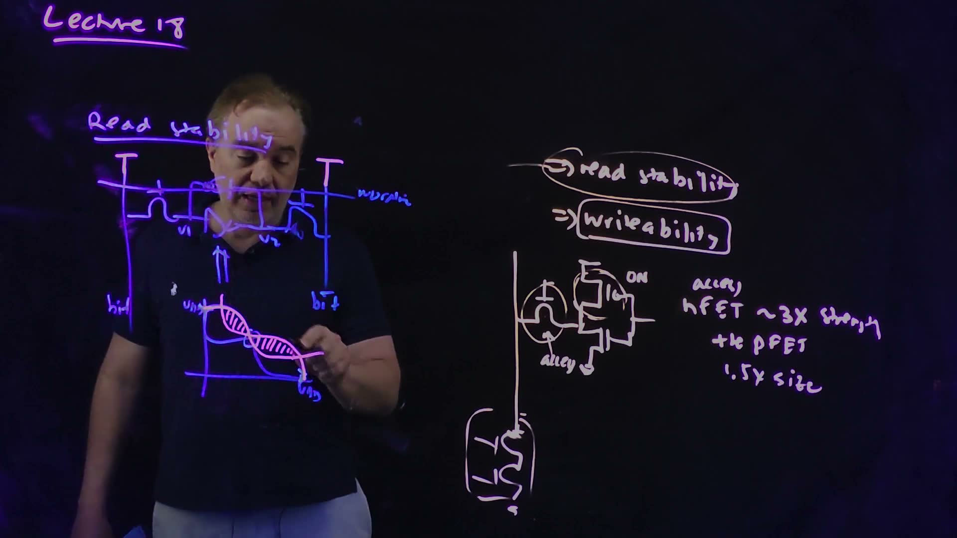
Six minimum-area devices leave two requirements board (L18 02:18):
- Read stability. Reading must not flip the cell. During a read the access device pushes current into the 0 node; the node must stay low (§3).
- Writability. Writing must flip the cell. During a write the access device must pull the 1 node down against the cell’s own PFET (§2).
Both are fights between the access transistor and a device inside the cell, and they ask opposite things of it: strong enough to win the write, weak enough to lose the read.
A worked example (the board’s sequences, with this guide’s labels). The cell holds , . In a read, which access device carries current? Only bit’s: its bitline is at and its node at 0, while ‘s device has on both sides. Bit falls, stays high. To write , pull low: now ‘s access device carries the current, from into the bitline, and bit’s device carries almost none until the cell flips.
Traps.
- “The word line selects a column.” It selects a row: every cell on it connects to its bitlines at once. The bitlines are the columns.
- “In a read both bitlines move.” Only the bitline on the side holding 0 falls.
- Reading the state from the wrong side. A 0 on shows as bit falling; a 0 on as falling.
Check yourself Why are both bitlines precharged high before a read, rather than low?
A low bitline would write the cell: on the side holding 1, the access device would pull that node down, exactly as a write does. A high bitline is harmless on the side holding 1 (no voltage across the access device) and only slightly disturbs the side holding 0, where the pull-down holds the node (§3). And a 0 node can pull a high bitline down, which is the read signal; it could not pull a low one any lower.
Check yourself (Two steps.) An array has 256 rows and 256 columns. How many access transistors connect to each bitline, and how many access-transistor gates load each word line?
Each bitline runs down one column and meets one cell per row, with one access device on its side: 256 drains per bitline. Each word line runs across a row and meets 256 cells, and each cell has two access devices with their gates on it: 512 gates per word line. §12 uses this count for the word line’s load.
Check yourself A cell holds V1 = 1. A write pulls bit low. What happens, and which device carries the current at first?
Bit’s access device conducts from into the low bitline, fighting the cell’s PFET that holds up. If the access path wins (§2), falls below the other inverter’s threshold, rises, and the cell flips to .
2. Writability: the access NFET must beat the cell’s PFET
You need
The write fight and its divider (Chapter 13 §7). When two on paths fight over one node, one from and one to ground, treat each as a resistor and the node sits at the divider’s voltage:
An NFET of width pulling down is ; a PFET of width pulling up is , because holes are about half as mobile as electrons, so a PFET must be twice as wide to be as strong (Chapter 7). Devices in series add. The write succeeds when falls below the switching threshold of the inverter the node drives. The model compares strengths; it does not predict exact voltages.
The cell (§1): two access NFETs () from bit and to and , and two inverters (PFET , pull-down NFET ).
The question. A write pulls one bitline to ground. The node on that side holds 1, and the cell’s own PFET is holding it there. Who must win, and by how much?
The fight
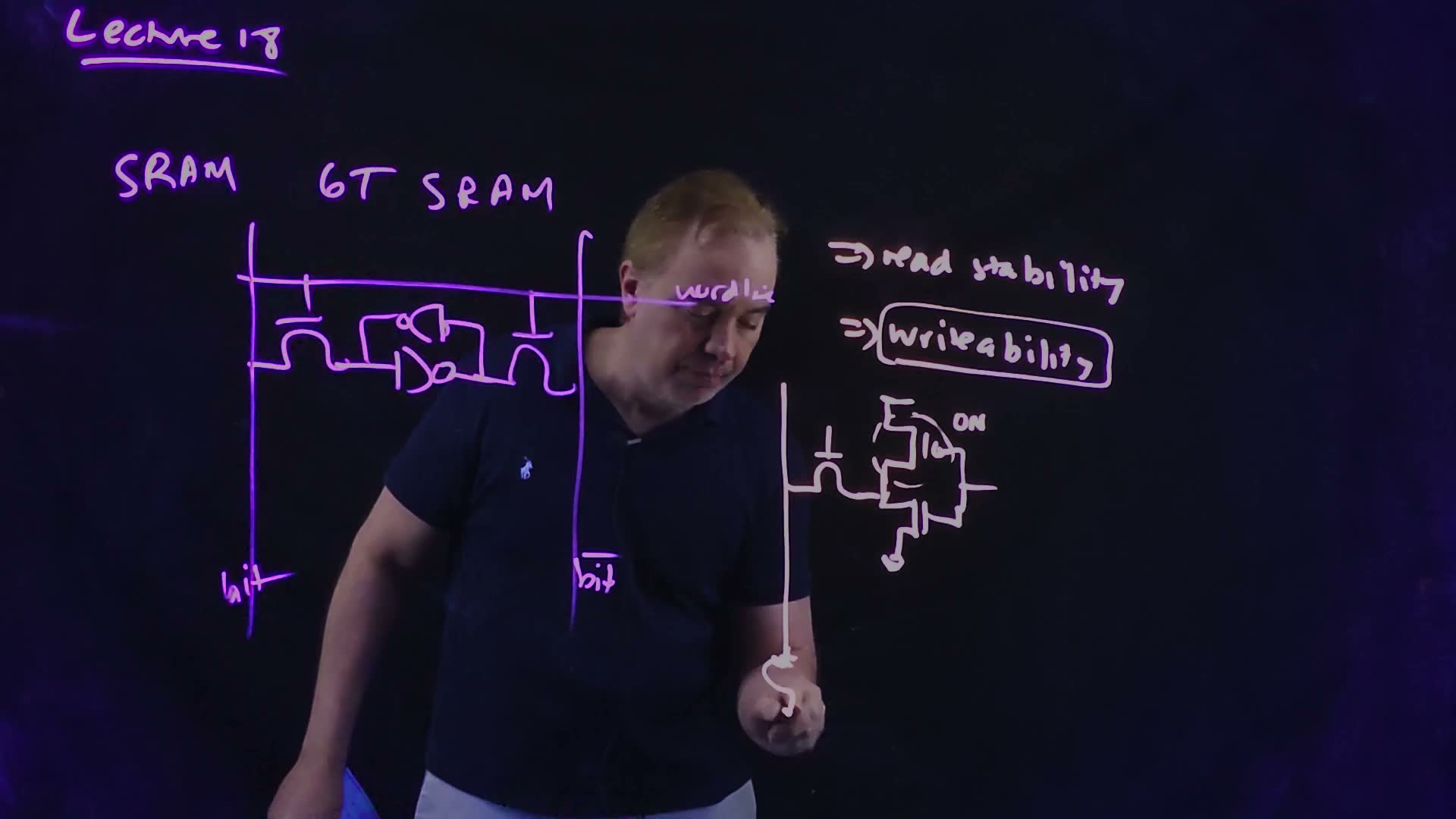
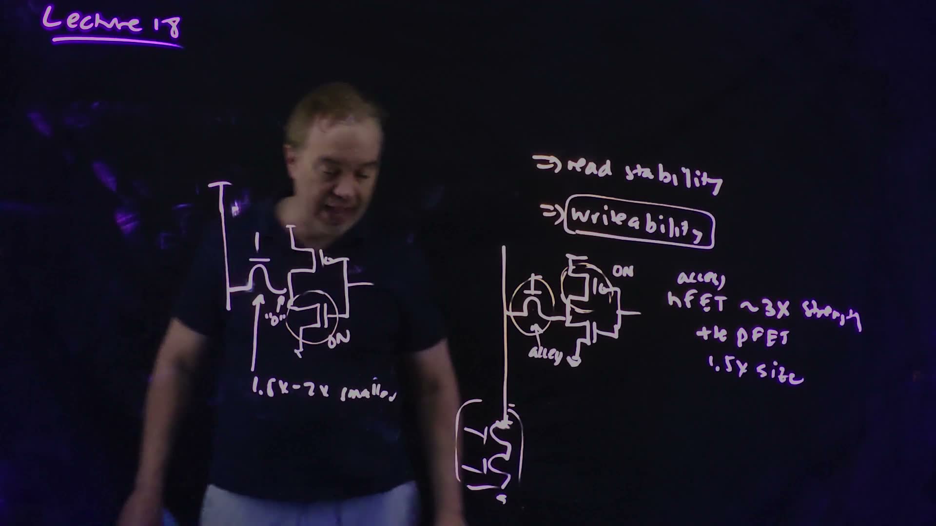
The writability fight (board, 02:12–04:30)
- The scene. Write a 0 into the node that holds 1, say . The driver at the bottom of the column pulls to ground through “a couple of transistors” (02:34; §8 builds them). The word line is high, so the access NFET connects to .
- Who holds the node up. is the output of the inverter whose input is . Its NFET is off, and its PFET is on: the board marks it “ON”. The PFET pulls toward .
- Who pulls it down. The access NFET, in series with the driver, pulls toward ground. “This path beats this one” (03:09): the access path must be the stronger, assuming the driver is strong.
- When it has won. need not reach 0. It must fall below the switching threshold of the inverter it drives; then rises, the PFET that was holding up turns off, and the loop finishes the flip by itself.
The writability fight, redrawn from the board (Lecture18 @ 04:20). (a) is pulled to ground by the two series NFETs of the write driver (gates at 1). The access NFET (gate WL = 1, width ) connects it to , which holds 1 and is being pulled down. The inverter driving is drawn as its devices: its PFET () is on and pulls up; its NFET is off (dashed); both gates are at . (b) The same fight as a divider added: from to , then and the driver’s resistance in series to ground.
The ratio: three times as strong, one and a half times as wide
The board’s rule board (04:20): “access nFET ~3X strength [of] the pFET, 1.5x size”. The lecturer first says “3x the size”, then corrects himself: “3x the strength, sorry, which means 1.5x the size difference, right? Because the PFET is going to be a weaker device” (04:06).
Why 3× strength is 1.5× width (derive)
- Strength per width. An NFET of width has resistance : strength . A PFET of width has : strength .
- Set the ratio. Access strength over PFET strength . The board wants 3.
- Solve. , so . A strength ratio and a width ratio differ by the mobility factor of 2.
Memorize the rule and its reason: access about 3× the PFET’s strength, 1.5× its width, because a PFET of the same width is half as strong.
How far down the node goes
The divider added (Chapter 13’s model) says where the node settles while the fight lasts. With an ideal driver (bitline at 0), and . At 3× strength, :
That is far below the switching threshold of the cell inverter the node drives, which sits below because the cell’s pull-down is far stronger than its PFET (§3): the write wins with margin. The margin matters because every device in series with the access NFET (the driver’s stack in §8, the column multiplexer in §9) adds to , and because the devices vary from cell to cell (§5).
Derive it on the exam in three lines: the PFET’s resistance, the pull-down path’s resistance (access plus every series device), the divider.
A worked example added (the example cell, for example: µm, µm).
The example cell's write
- Pull-up. The PFET: .
- Pull-down, ideal driver. The access NFET alone: .
- Divider. : the board’s ratio gives a quarter of the supply.
- Without the ratio. Make the access NFET as wide as the PFET, µm: and . Still below in this crude model, but closer to that lowered threshold , with less room for the driver, the multiplexer and the device spread.
The board (Lecture18 @ 04:20)
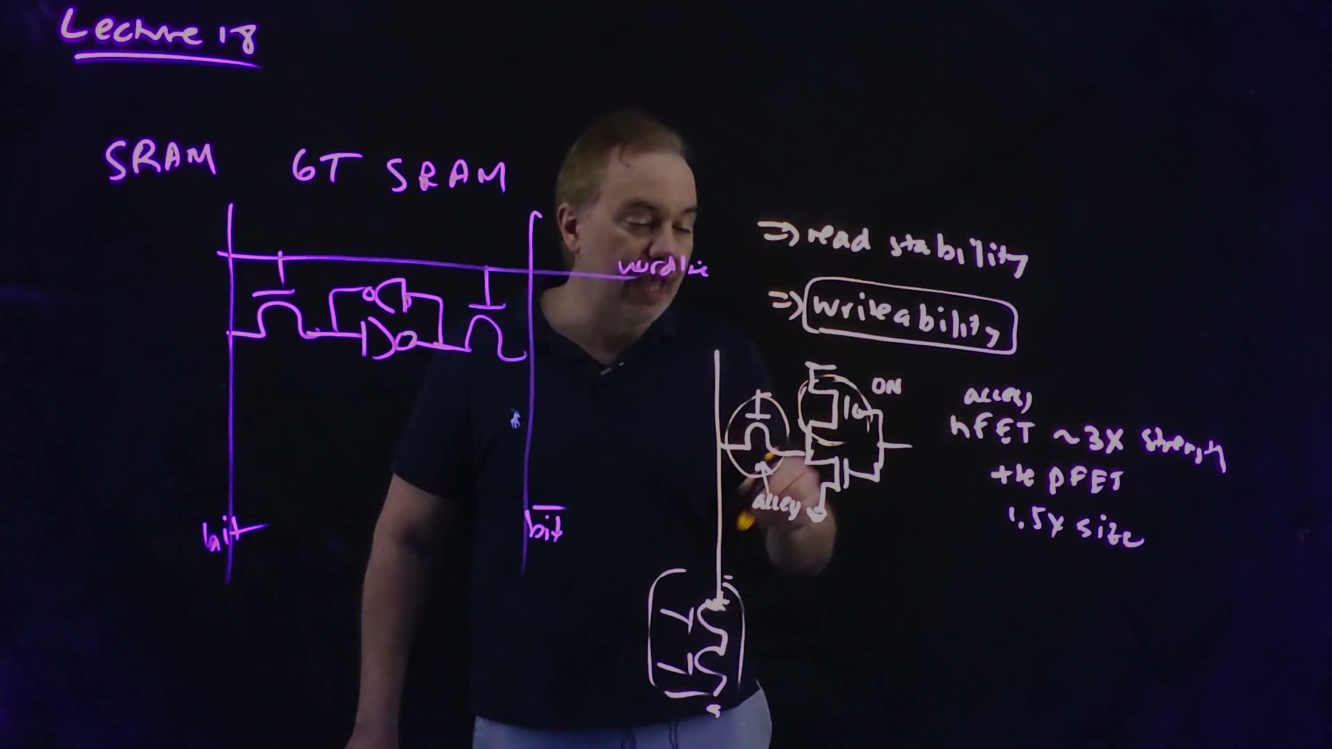
Fair copy of the board above (Lecture18 @ 04:20), mark for mark in its own layout. All black: a violet pen wrote the title, “SRAM”, “6T SRAM” and the cell; a pale cream pen wrote everything from “read stability” on. The cream writes the next topic beside the cell rather than a layer over it, so it takes no accent. The board draws each transistor as a gate bar beside a channel bump, a supply as a short T bar and ground as a small triangle. In the sketch, the access NFET and the cell’s PFET (marked ON) are ringed separately, and the two-NFET stack at the foot of the bitline is ringed too. “wordline”, washed out by the lecturer’s face here, is read on 01:33; the “access” label and the lower edge of its ring, under his hand, on 06:40.
Traps.
- Reading “3X” as a width ratio. 3× is the strength; the width ratio is 1.5×.
- A stronger PFET “to hold the data better.” The cell’s PFET is exactly the device the write must overpower; strengthening it makes the cell unwritable.
- The access NFET alone. It does not fight alone: the driver’s devices are in series with it, and each one raises .
Check yourself If a PFET were a third as strong as an NFET of the same width, what width ratio Wa/Wp would make the access NFET 3× as strong as the PFET?
Access strength over PFET strength , so 1.0.
Check yourself (Two steps.) For example: the example cell (Wp = 0.2 µm, Wa = 0.3 µm) is written through two series 0.6 µm NFETs below the access device. Where does the node settle?
Pull-down: . Pull-up: . Divider: 0.40 , up from 0.25 with an ideal driver: the series devices ate more than half the margin to , which is smaller than the 0.25 to .
3. Read stability: the access NFET must lose to the pull-down
You need
The divider (§2; Chapter 13’s model). Two on paths fighting over a node leave it at , with for an NFET pulling down. Rough: it compares strengths.
An NFET pulling up is weak (Chapter 13 §7). Its source is the node it is raising, so its gate-to-source voltage shrinks as the node rises, and it cannot pull higher than . The course’s estimate treats it as , like a PFET.
The switching threshold (Chapter 6). An inverter’s output flips when its input crosses : near for a balanced inverter, lower when its NFET is the stronger device.
The question. During a read the bitline sits at and the access device connects it to the node that holds 0. That node’s pull-down holds it at ground. How high does the node rise, and what keeps it from flipping the cell?
The fight
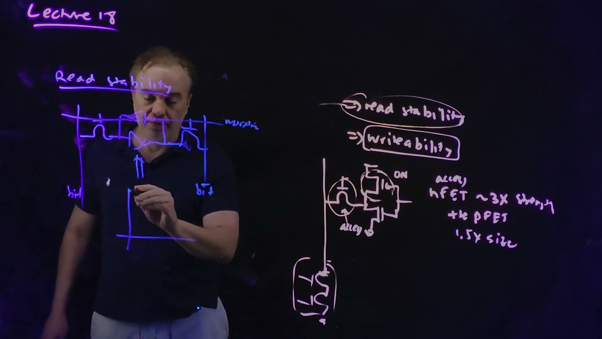
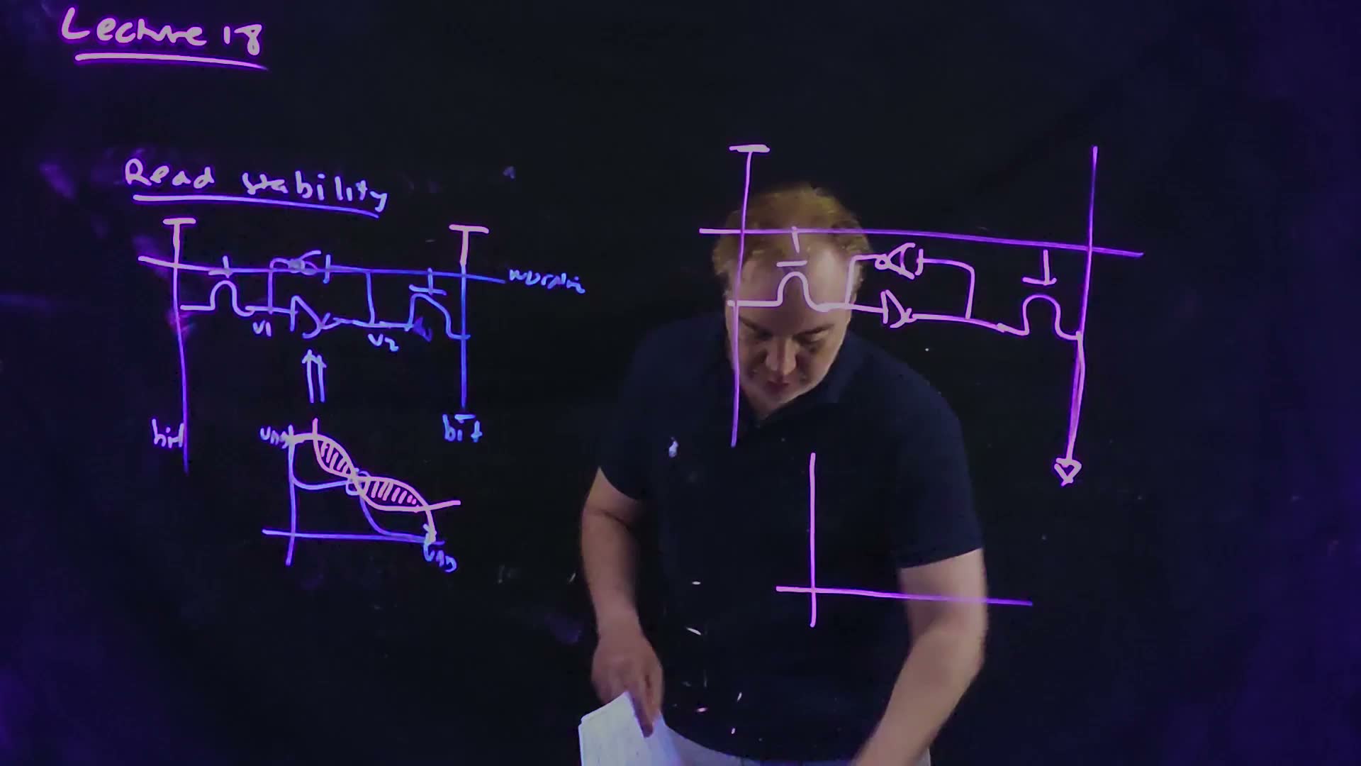
The read-stability fight (board, 04:40–06:40)
- The scene. The bitline was precharged to (the board draws its precharge device at the top). The word line is high (“1”). The node holds 0 (“0”), and the inverter driving it has its pull-down NFET on (the board marks it “ON”), because that inverter’s input is the other node, at 1.
- The fight. Current flows from the bitline, through the access NFET, into the node, and through the pull-down to ground. The node is the middle of a divider: the access NFET pulls it up, the pull-down pulls it down.
- The danger. The node rises a little. If it rises past the threshold of the inverter it drives, that inverter’s output (the other node, at 1) starts to fall, which turns the pull-down off, and the read flips the cell.
- The rule. “Weaken this path relative to this one” (05:56): the access NFET must be the weaker, “1.5 to 2x smaller … than the NFET” (06:23). Both are NFETs, so the width ratio is the strength ratio.
The read-stability fight, redrawn from the board (Lecture18 @ 06:40). (a) bit is precharged to . The access NFET (gate WL = 1, width ) connects it to , which holds 0 and is pushed up. The inverter driving is drawn as its devices: the pull-down NFET () is on and holds low; the PFET is off (dashed); both gates are at . (b) The divider added: from to , then to ground.
How high the node rises
The read bump as a divider (derive)
- Pull-down. The pull-down NFET pulls down: .
- Pull-up. The access NFET pulls up, so it is weak: .
- Divider. . Divide top and bottom by and write : .
The board’s range: gives , gives . With equal widths, , the node would reach .
Why the margin matters more than the bare number. The cell’s inverters are skewed: their pull-down NFET is the strongest device in the cell and their PFET the weakest, so their threshold sits well below (the skew argument of Chapter 11 §7, in reverse). The bump must stay below that lowered threshold, and random variation (§5) moves the threshold further from cell to cell.
Memorize the rule; derive the bump in three lines (above).
Both rules together
§2 says the access NFET must be about 3× as strong as the PFET; this section says the pull-down must be 1.5–2× as strong as the access NFET. Together they order the cell’s three devices:
The two rules constrain different pairs (access against PFET, access against pull-down), so they never conflict. With such tiny devices, reaching the ratios can take “non-minimum length” on some of them (15:33): a longer channel makes a device weaker without making it narrower than the rules allow.
Memorize the order: pull-down strongest, access in the middle, PFET weakest.
The example cell’s sizes added (for example; the ratios are the board’s, Lecture18 @ 04:20 and 06:40): the six-transistor cell with PFETs of 0.2 µm, access NFETs of 0.3 µm and pull-down NFETs of 0.6 µm. One bracket joins an access NFET and the PFET on the same node, (the write fight); the other joins the same access NFET and the pull-down, (the read fight).
A worked example added (the example cell, for example). , so , which is 0.20 V at V. On a past final (FN10-5b) the cell’s NFETs are both 1 µm, so and the bump would be : that cell ignores the read rule. The question asks only for the bitline’s delay, which depends on the series path of the two NFETs, not on where the node settles, so the estimate does not care.
The board (Lecture18 @ 06:40)
Fair copy of the board above (Lecture18 @ 06:40), mark for mark in its own layout, on the coordinates of the 04:20 copy: the right half is that board’s, unchanged. All black: only “Lecture 18” is in the violet pen; the pale cream pen wrote the rest. The cell, “SRAM” and “6T SRAM” have been erased, and the read-stability sketch stands in their place. The quoted “0” at the node, with the short stroke and dot beside it, is copied as drawn.
Traps.
- A stronger access NFET to speed the read. It discharges the bitline faster and lifts the 0 node higher: the read gets faster and less stable.
- for the access NFET pulling up. It pulls up weakly, about . With the estimate for would be , past the cell’s lowered threshold; with it is .
- “The two rules conflict.” They constrain different pairs and are met together by the order pull-down > access > PFET.
Check yourself What cell ratio β keeps the read bump below 0.15 VDD?
means , so 2.83: beyond the board’s 1.5–2.
Check yourself (Two steps.) For example: a designer widens the example cell's access NFETs from 0.3 to 0.45 µm to speed reads (Wpd = 0.6 µm, Wp = 0.2 µm). What happens to the read bump, and to §2's VX with an ideal driver?
Read: , 0.27 , up from 0.20. Write: , , 0.18 , down from 0.25. The wider access device writes more easily and reads less safely: the two requirements pull it in opposite directions.
4. The butterfly: hold, read and write
You need
The butterfly diagram (Chapter 13 §5). Plot one inverter’s transfer curve, against , and on the same axes the other inverter’s, mirrored ( against ). Where the two curves cross, each inverter’s output is the other’s input: the loop’s equilibria. A storage loop has three crossings: two stable states at the corners and a metastable one in the middle. The curves enclose two eye-shaped lobes, the “wings”.
A write on the butterfly (Chapter 13 §7). A writer fighting one inverter squashes that inverter’s curve; when the squashed curve no longer reaches the old state’s corner, only one crossing is left and the loop must go there.
The two dividers (§2, §3). During a read each 0 node rises to ; during a write the node being pulled down settles at , for the example cell with an ideal driver.
The question. §2 and §3 looked at one node in one fight. What do the two fights do to the whole loop, and how can one number say how safe a read is?
Hold, then read
The sketches here use Chapter 13’s drawing aid added, an S-curve for each inverter. It is a picture, not a device model; only the lifted lows and capped highs come from the dividers.
From hold to read (board, 07:41–10:11)
- Hold. The word line is low, both access devices are off, and the cell is Chapter 13’s loop: “a bistable … a metastable state here … two stable states” (07:41–08:27). The thin curves in the figure: two lobes, three crossings.
- Read. Both access devices turn on, with both bitlines at . Whichever node is low is now pushed up by its access device: that inverter’s low output is lifted to , for . Both inverters are affected (either node can be the low one), so both curves’ low ends rise. The thick curves: “the wings … are going to get smaller” (08:28–09:41).
- Measure the wings. “The largest square that I can fit inside of these butterfly wings is … quantitatively a way that people look at the noise margins of SRAM cells” (09:41). The side of that square is the static noise margin (SNM) added (the name is the textbooks’): a noise voltage smaller than the side cannot push the loop out of its lobe. In the sketch, the hold square is and the read square, for , .
- Squeeze to nothing. A weaker pull-down lifts the lows further. For the read square is ; for , . If a lobe closes, the read has only one stable crossing left: reading the cell writes it.
Hold and read on the butterfly added, computed from Chapter 13’s drawing aid with the read low lifted to (§3’s divider, ); a sketch, not a device model. Axes across and up, to . Thin: the hold curves. Thick: the read curves, whose low ends sit at . The largest square in each lobe: dashed for hold (side ), solid for read (side ). Dots mark the read curves’ crossings: two stable (filled), one metastable (hollow).
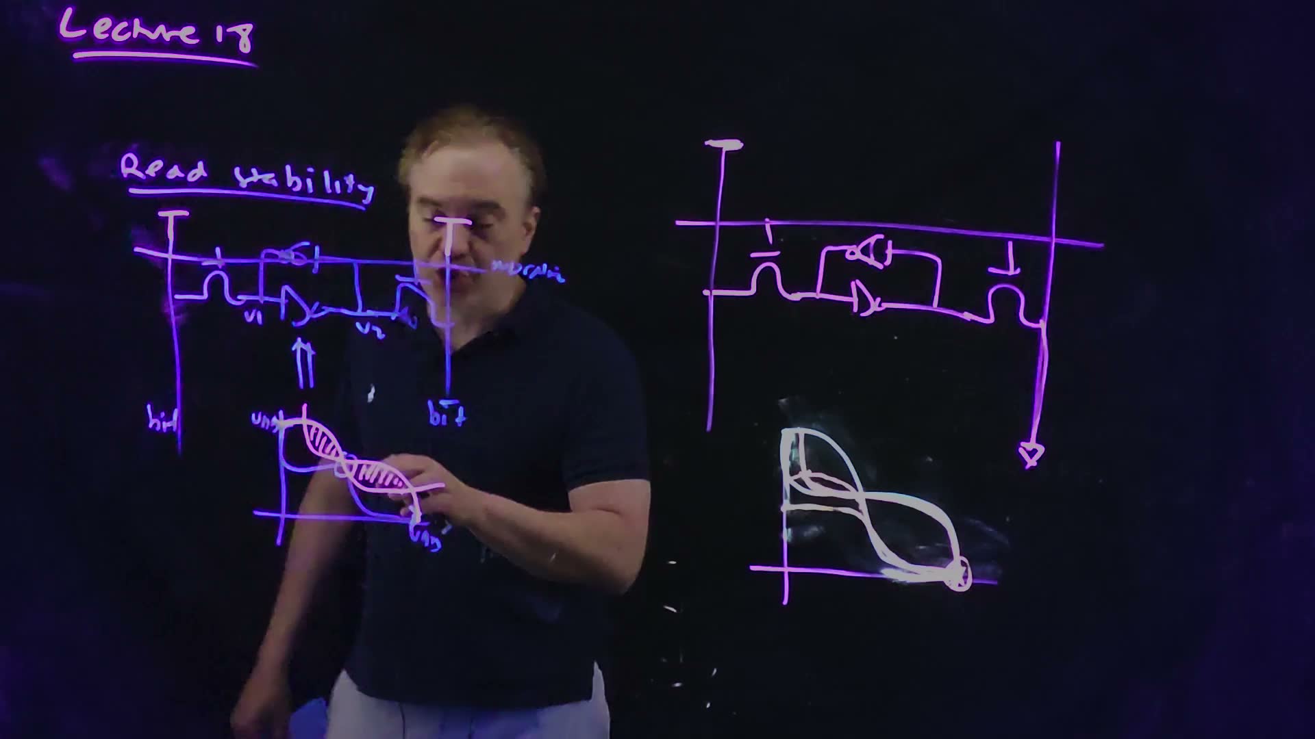
The board (Lecture18 @ 19:23)
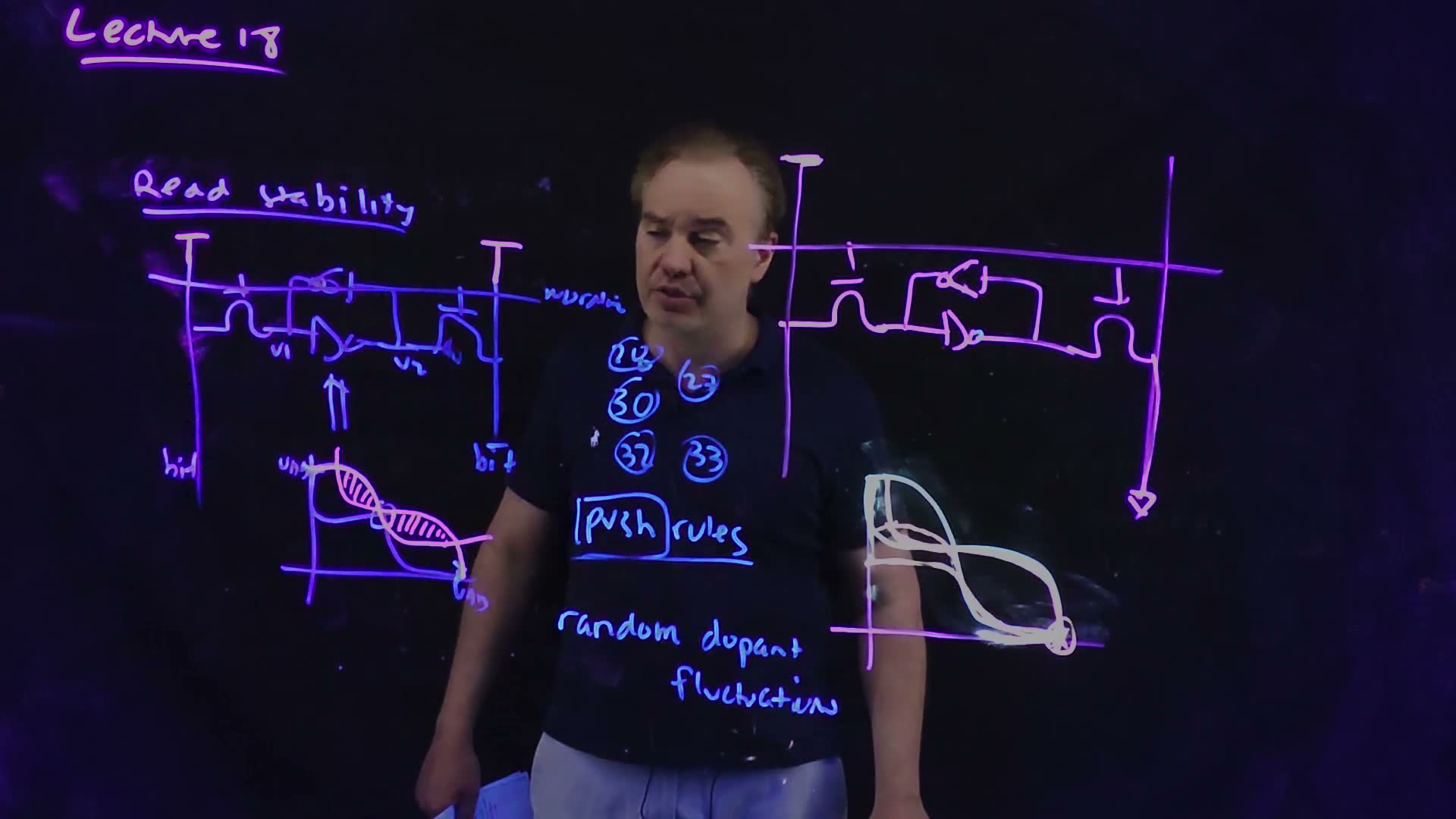
Fair copy of the board above (Lecture18 @ 19:23), mark for mark in its own layout. Black is the violet pen: both cells, the hold butterfly and both pairs of axes. It also stands for the blue pen of the variability notes in the middle, which writes the next topic beside the drawings rather than a layer over them. Magenta is the pink pen, the read layer: the precharge T’s on the read cell’s bitlines, the two read curves and the hatching of their lobes. Orange is the pale cream pen, the write layer: the T on the write cell’s bit, the write butterfly and the ring on its single crossing. The write butterfly was drawn, wiped and redrawn, and its smeared strokes are copied as strokes. The ringed numbers are dopant counts (Section 5).
Write
The write on the butterfly (board, 10:47–13:30)
- The scene. To write into a cell that holds , pull bit low and keep at its precharge (the mirror of §2’s scene, which wrote through ).
- The side behaves as in a read. Its access device sees a high bitline, so the curve of the inverter driving has its low end lifted, as in step 2 above.
- The bit side is capped. The inverter driving is fighting the low bitline: its output can rise only to the divider’s level, it “is only going to be able to make it up to this” (12:31). Its curve is squashed down to , for the example cell.
- One crossing. The capped curve no longer reaches the upper-left corner, so the old state’s lobe has vanished. One crossing remains, near , : the new state. The cell is written.
- A failed write. “If for some reason … I still have these two states, then … that cell is not writable” (13:00–13:30). In the sketch, a cap of (a far too weak access path) leaves three crossings, and the old state at survives. The change from one crossing to three happens between and in this sketch: an illustration, not a design number.
The write on the butterfly added, computed from the drawing aid (a sketch, not a device model). In both panels the curve of the inverter driving is read-lifted (, thin); the curve of the inverter driving is shown undisturbed (dashed grey) and capped at (thick). Left, (§2’s divider): one crossing, the new state , . Right, : three crossings, and the old state (, ) survives: not writable.
“In read stability, I don’t want the butterfly diagram to pull apart. In writability, I do” (13:30). A read must leave both lobes open; a write must close one.
Memorize the definition: the static noise margin is the side of the largest square that fits in the smaller lobe of the read butterfly. Remember that the numbers in these sketches are not device numbers.
Try it added. The widget sets the three widths of the cell. The read lift and the write cap come from §2’s and §3’s dividers, and the curves are the drawing aid. Widen the access NFET and watch the read square shrink while the write gets easier. The PFET alone cannot break the write from these widths: at the slider’s end, 0.60 µm, , and the sketch still writes. Narrow the access NFET to 0.10 µm first; then a PFET of 0.40 µm gives , and the write fails.
Traps.
- The hold square as the margin. The read is the worst case: its lobes are smaller. The SNM that matters is the read SNM.
- “In a write one curve moves.” Both change: one is read-lifted, the other collapses.
- The sketch’s threshold as a design limit. The 0.71–0.72 comes from the drawing aid’s steepness; real curves move it.
Check yourself During a read, only bit̄ is precharged (bit is left floating at 0 V by mistake). Which part of the read butterfly would still change as in §4, and why is the cell in danger anyway?
Only the inverter whose 0 node sits on the side gets its low lifted by a high bitline, so only the curve of the inverter driving is lifted. But the bit side now has a low bitline on an open access device: if holds 1, that is a write. The precharge of both lines is what makes a read a read.
Check yourself (Two steps.) With β = 1.5, where is the read's lifted low VL, and does the read square rise or fall against β = 2?
0.25 , higher than 0.20. The lows rise further, the lobes shrink, and the read square falls: 0.103 against 0.127 in the sketch.
5. Variability, push rules and the remedies
You need
The threshold depends on the dopants under the gate (Chapter 6 §8). A transistor’s threshold voltage is set by the charge of the dopant atoms in its channel region. Devices drawn alike are not quite alike: their thresholds scatter, and so do their strengths.
The read square (§4). The static noise margin is the side of the largest square in the smaller lobe of the read butterfly; it shrinks as the read lifts the lows.
The question. §2–§4 set the cell’s ratios on nominal devices. Why does a cell drawn with the right ratios still fail, at random, one in a million?
Push rules and tiny devices
SRAM cells are drawn with push rules board (14:28–15:33): design rules the foundry tunes for the SRAM cell alone, tighter than the rules for “normal logic”. The cell’s devices are the smallest on the chip, sometimes with non-minimum lengths to reach the ratios.
Countable dopants
Random dopant fluctuation (board, 15:53–16:43)
- Count them. In a tiny device the dopant atoms under the gate are few enough to count. “Say I have … 30 … dopants … Some device might have 28, some … 32, some … 27, some … 33” (16:11; the board rings 28, 27, 30, 32, 33).
- How big the spread is added. For atoms placed at random, the count scatters by about the square root of its mean (Poisson statistics, background): , an 18 % spread. So 27 and 33 are ordinary, not rare.
- Each count gives its own threshold. The two inverters of one cell no longer match, and the access device no longer has its nominal strength against its neighbours.
- Margins rest on ratios. §2–§4’s margins are ratios of strengths. A random mismatch can close the read lobe or keep the write’s old crossing in a single cell, and in an array of millions some cell is that unlucky one.
A mismatched cell during a read added, computed from Chapter 13’s drawing aid (a sketch, not a device model). Both curves are read-lifted to , but the inverter driving has its threshold moved from to ; its undisturbed symmetric read curve is dashed grey. The lobes are no longer equal: the upper-left square has side , the lower-right . The cell’s margin is the smaller.
A worked example added. Shift one inverter’s threshold by in the read sketch with . The symmetric cell had two squares of ; the mismatched one has and . Its noise margin is the smaller, : half the nominal, from one shift.
The remedies
In the lecturer’s order (speech, 17:25–19:45):
- More transistors per cell. Eight- and ten-transistor cells separate the read path from the cell’s nodes. “None of them have really caught on” (the density cost).
- Bigger devices. Fewer dopants matter less in a bigger device, but the cell grows: “highly undesirable”.
- Redundancy. Build spare cells; a self-check after manufacture finds the cells that fail and swaps in the spares (18:11).
- Supply tricks. Raise the cell’s supply during an access, which strengthens it for the read; lower it while the cell only retains data, so “the leakage power … is more controlled” (18:37).
“Six transistor cells continue to be used, and these other tricks are employed” (19:12). This term’s class makes the same point about few dopants in small devices (Fall 2026 Lecture 2), and about SRAM’s sensitivity to relative strengths at skewed corners (Lecture 5).
Traps.
- “A cell that meets the ratios always works.” The ratios are nominal; mismatch is random and per cell.
- “Bigger is free.” Every remedy that grows the cell is multiplied by the whole array; that is why the periphery does most of the work.
Check yourself Why does raising the cell's supply only during an access help, without costing much leakage?
Leakage is paid all the time, by every cell. The boost lasts only for the access, and only the accessed row needs it; the rest of the time the supply can even be lowered to save leakage while the cells retain their data.
Check yourself (Two steps.) In the mismatched read sketch, which stored state is the vulnerable one, and in which operation?
The vulnerable state is the one whose lobe is smaller: the upper-left lobe, high and low, with a square of . It is vulnerable during a read, when the lows are lifted; in hold the lobes are larger.
6. Two phases for the periphery: precharge and access
You need
Two-phase clocks (Chapter 14 §3). Two clocks, and , are high in turn and never together. Between falling and rising, and between falling and rising, both are low: the non-overlap gaps. A generator can widen them on purpose.
The question. The cell needs its bitlines precharged before every access, and the access must not start until the precharge has stopped. How does one clock cycle organize the two?
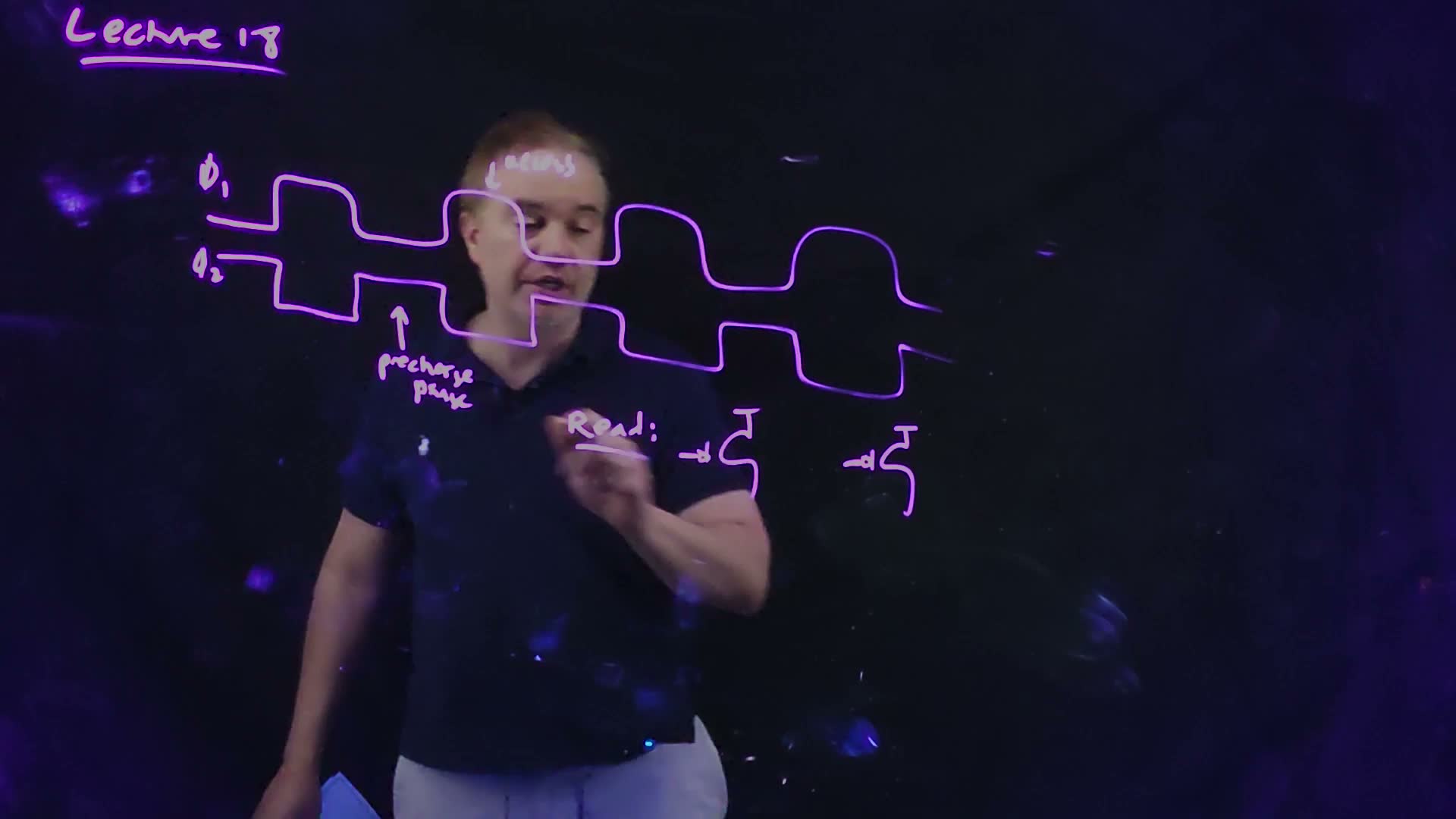
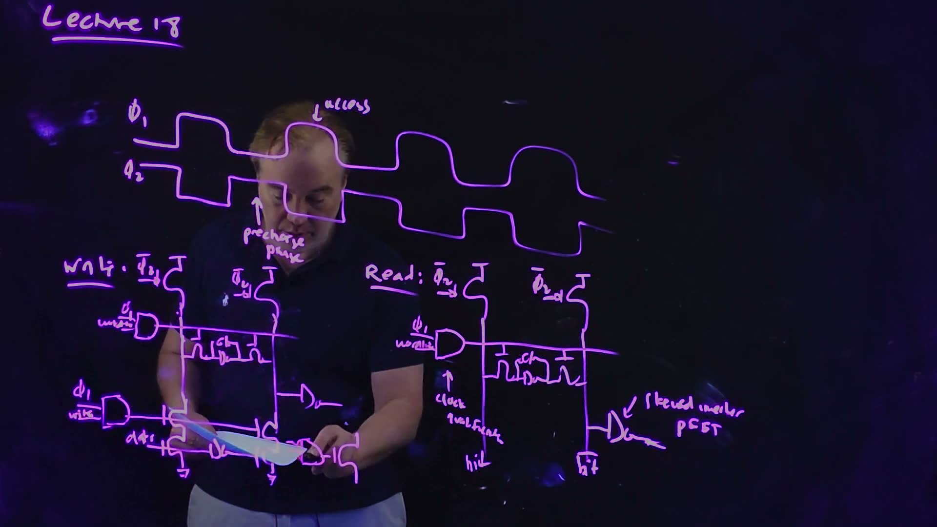
Precharge and access (board, 20:09–22:16)
- Two phases. The read and write circuits, “the data path for the SRAM”, run on two clocks “nominally 180 degrees out of phase” (20:09). While is high the bitlines precharge; while is high the cell is accessed: its word line is up, and it is read or written.
- Precharge on . The precharge PFETs pull the bitlines to . Their gates are driven by , so they are on exactly while is high.
- Why not . With ideal complementary clocks, and are the same signal. Driving the precharge from gives “the ability, should I choose to, to create non-overlap windows between φ1 and φ2” (21:48–22:16).
- The gap. added With a gap, precharge ends when falls, and the word line can rise only when rises; between them sits , when neither is on. §12 spends that gap.
The two phases of the periphery, redrawn from the board (Lecture18 @ 21:42) with non-overlap gaps added (the board draws the clocks complementary). Rows , and over two cycles. Brackets mark each high (the access phase) and each high (the precharge phase). marks the gap from falling to rising.
A worked example added (§12’s example decoder). Its stages I–III must finish between falling and rising, and they take : the gap must be . The precharge on has stopped by then, so the whole gap is the decoder’s (Check 1). The other numbers come with the circuits, §7–§12.
Traps.
- Precharging on “because it is the same”. Only while the clocks are exactly complementary; with a gap, the choice decides what the gap can be used for.
- Precharge PFETs with on the gate. A PFET is on when its gate is low; to be on during it needs .
Check yourself (Two steps.) Suppose the precharge PFETs were driven by φ1 (on while φ1 is low) and the word line by φ1. Does this work with complementary clocks, and what changes when a gap is added?
With complementary clocks, “ low” is exactly “ high”, so the precharge stops as the access starts: it works. With a gap, the precharge (on whenever is low) now also runs through both gaps; it still stops when the word line rises, but the gap can no longer separate the end of precharge from the start of the access. The precharge-on- version ends the precharge at falling, a whole before the access, and that time is free for the decoder (§12).
Check yourself What would happen if the precharge PFETs were still on when the word line rose?
They would hold the bitlines at while the cell tried to pull one down: the read signal would fight the precharge and never develop, and a write driver would fight it too, burning current.
7. Reading a column: the clock-qualified word line and the skewed inverter
You need
A stage’s delay from its gain (Chapter 8 §1). A stage’s delay, in units of the fan-out-of-one delay , is its gain: the capacitance it drives divided by the input capacitance of the normalized inverter, the inverter with the same pull-down strength (NFET , PFET , input ). Devices in series combine like resistors: . Capacitances can be counted in µm of gate width, with fF/µm. The delay is to the 50 % point.
Skewed inverters (Chapter 11 §7). Making one device much stronger than the other moves the switching threshold toward that device’s rail: a strong PFET moves it up toward .
The two phases (§6): precharge while is high, access while is high.
The question. How does a column read its cell: what turns the word line on at the right time, what detects the falling bitline, and how long does the bitline take?
The read column
The read circuit (board, 22:16–24:31)
- Precharge. Two PFETs, gates on , pull bit and to during .
- A clock-qualified word line. The row decoder’s output for this row is ANDed with before it drives the word line. “Clock qualification … basically it’s a glorified term for AND” (22:44). The decoder’s output may be valid (or still changing) during precharge; the AND keeps the word line down until the access phase.
- A single-ended detector. An inverter hangs from . It is skewed: its PFET “much stronger than the NFET … to move the switch point toward VDD” (23:44–24:31). A small sag on already flips it.
- Its polarity. “The bit bar is actually flipped here”: the inverter on outputs the sense of the bit side. If holds 0, falls and the output goes to 1; if holds 1, stays high and the output stays 0.
The read column, redrawn from the board (Lecture18 @ 23:56). Precharge PFETs on at the tops of bit and ; the word line driven by an AND of and the decoder’s row select (the clock qualification; is this guide’s label); one cell and “⋮” for the others; at the foot of a skewed inverter, , to the output.
The board (Lecture18 @ 23:56)
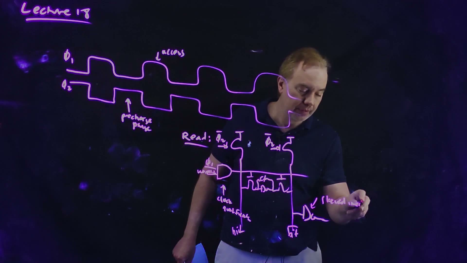
Fair copy of the board above (Lecture18 @ 23:56), mark for mark in its own layout, all in black: one violet pen wrote the board. “skewed inv” is copied as written so far; by 25:40 it reads “skewed inverter”, with “PFET” under it. The clocks’ last cycle, washed out by the lecturer’s face here, is read on 25:40. The board draws each precharge PFET as an S-shaped channel with a bubble on its gate bar, and the cell’s devices as bumps under T-shaped gates.
How long the bitline takes
The bitline is long and heavily loaded; the cell that discharges it is tiny. Treat the discharge as one gate stage added.
The bitline as a gate stage (derive)
- The drive. The current flows through the access NFET and the pull-down NFET in series. Their equivalent width is .
- The normalized inverter. An inverter with this pull-down strength has input .
- The load. The bitline’s capacitance, in µm of gate: .
- The delay. To : , in .
- A smaller swing. Near the cell’s current is roughly constant, so the bitline falls roughly linearly, and the time is proportional to the swing: a detector that switches after needs .
Derive both, from Chapter 8 §1 and the constant-current picture.
A worked example added (the example column, for example: µm, µm, fF, fF/µm).
The example column's read
- Series width. µm.
- Normalized input. µm.
- Load. µm.
- To . .
- With the skewed inverter. If it switches at , the bitline needs to fall only instead of : , 0.4 of the time.
A past final asks this estimate for its own cell and bitline (FN10-5b); the memory practice page (FM1) solves it.
Traps.
- The access device alone. The pull-down is in series with it; is smaller than either width.
- The wrong swing. is to ; a detector that switches elsewhere needs the swing it actually waits for.
- The polarity. The detector sits on ; its output is the bit side’s value. Trace one stored value through before writing a waveform.
Check yourself Why does the AND of the word line with φ1 matter even when the decoder's output is already correct?
The decoder’s output can be valid, or still changing, during precharge. Without the AND, the word line would rise while the precharge PFETs are still on: the cell would fight the precharge, and a changing address could open the wrong row. The AND confines the access to .
Check yourself (Two steps.) For example: double the example column's rows, so the bitline is 240 fF. What are the bitline's time to VDD/2 and the time with the skewed inverter at 0.8 VDD?
Load: µm over the same µm normalized input: 200 . With the skewed inverter: 80 . The delay grows linearly with the rows: the reason arrays are cut into banks (§13).
8. Writing a column: the stack, the one-device driver and φ1-stable data
You need
The write fight (§2). The node that holds 1 is pulled down through the access NFET and every series device below it, against the cell’s PFET:
Each series device raises toward the threshold.
Latches (Chapter 13 §2). A latch clocked by is transparent while is high and holds while it is low, so its output cannot change during .
The question. What pulls the bitline low for a write, gated so that it acts only during the access and only on the right side, and how many devices may it put in series with the access NFET?
The two-high stack
The write column (board, 25:03–27:40)
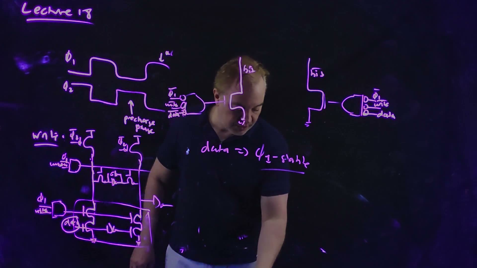
- The column as for a read. Precharge PFETs on ; the word line from the AND of and the row’s decode; the read inverter on .
- A stack on each bitline. Two NFETs in series from the bitline to ground. The upper one’s gate comes from an AND of and write; the lower one’s gate is data on the bit side and (data through an inverter) on the side.
- Write = 0. Both upper NFETs are off: the column only reads.
- Write = 1, during . The upper NFETs are on, and data picks the side: data = 1 pulls bit low, data = 0 pulls low.
The polarity, traced board (the board’s wiring, as FN17-6 prints it). Data = 1 pulls bit low, so the cell’s bit-side node takes 0 and takes 1. A later read: , so stays high, and the read inverter on outputs 0. The column returns the complement of the data written. That is harmless (the next stage can invert, or the wiring can swap data and , or the detector can sit on bit), but a waveform question built on this circuit expects it: data_in high, data_out low.
Fewer devices in series
The stack is two devices in series below the access NFET, and the column multiplexer (§9) adds a third. Each one raises . The lecture collapses each side to one NFET, and moves the logic into a gate that drives it board (27:41–29:45):
- bit’s NFET is driven by NOR(, , );
- ‘s NFET by NOR(, , data).
The board draws each NOR as an AND with bubbled inputs. By De Morgan, a NOR of complements is the AND of the true signals:
Derive it in one line. The driver is on only when , write = 1 and data = 1: the stack’s function with one device in the bitline’s path. The NOR switches on ‘s rising edge, in parallel with the word line’s AND, as the stack’s AND(, write) did; it adds no gate to the clock path and removes a device from the bitline’s.
The write column, redrawn from the board (Lecture18 @ 27:40 and 31:37). (a) The stacks: precharge PFETs on , the word line from an AND of and , one cell, and at the foot of each bitline two series NFETs to ground, the upper gates from an AND of and write, the lower gates data (bit side) and ( side); the read inverter on . (b) One device per side: bit’s NFET driven by NOR(, , ), ‘s by NOR(, , data) (the board’s bubbled-input ANDs, drawn as NORs). (c) The data comes from a latch clocked by .
A worked example added (the example cell, for example: µm, µm, each write-path device 0.6 µm; , the access NFET , each 0.6 µm device ).
The written node with each write path
- Two-high stack. : .
- Stack plus a mux device (§9). : : at or past the cell’s lowered threshold , so the write may fail.
- One NOR-driven device. : .
- One device plus a mux device. : , as good as the stack without a mux.
Removing one series device buys back exactly what the multiplexer costs.
φ1-stable data
The data must not change while is high board (29:56–31:37: “data ⇒ -stable”, boxed). If it changed during the access, the driver would switch sides halfway through a write, and the cell could be left with the wrong value or half-written. The board’s answer: take data from a latch clocked by (“D Q”, ). That latch changes only while is high, so its output is still throughout : Chapter 13’s two-phase discipline.
The board (Lecture18 @ 31:37)
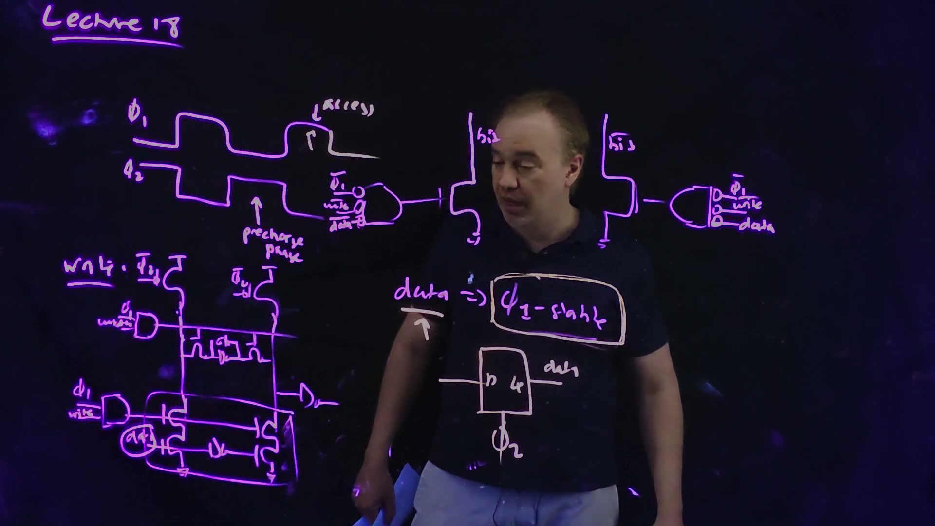
Fair copy of the board above (Lecture18 @ 31:37), mark for mark in its own layout, all in black: one violet pen wrote the board, the ring on “data” and the loop round the write devices included. The one-device drivers and the boxed “-stable”, behind the lecturer here, show through and need no restoring (the same on 31:02). The clocks keep their first cycle and a half from 23:56; the tails were wiped and redrawn short. The board draws the drivers’ NORs as ANDs with bubbled inputs (Section 8), and grounds as small triangles. The ring on “data” is drawn wider than the board’s, to hold the typeset word.
Traps.
- The polarity reversed. Data drives the bit side’s device in the board’s circuit; trace one value (data = 1 → bit low → ) before drawing a waveform.
- Data from a latch. It changes during the access, exactly when it must be still.
- “The NOR slows the write.” It switches on ‘s rising edge, in parallel with the word line’s AND, as the stack’s AND(, write) did: it adds no gate to the clock path, and it takes a device out of the bitline’s.
Check yourself (Two steps.) Write = 1, data = 0, φ1 = 1, with the board's one-device drivers. Which NFET conducts, which bitline falls, and what does the read inverter output on the next read of that cell?
bit’s NOR has inputs , , : output 0, off. ’s NOR has inputs 0, 0, data = 0: output 1, so ‘s NFET conducts and falls. The cell takes , . On the next read, pulls down and the inverter on it outputs 1: the complement of data = 0.
Check yourself Why must the driver's NOR include φ̄1, when the word line is already qualified by φ1?
Without it the driver would pull its bitline low whenever write and data are set, including during the precharge phase: it would fight the precharge PFETs, burn current, and leave the bitline low when the next access began.
9. Column multiplexing: the circuit and its cost
You need
The address split (Chapter 18 §10 teaches it). A memory of words of bits built as rows by columns () holds words on each row. Its address bits split as : the row bits go to the row decoder, the column bits choose one of the words through a :1 column multiplexer. Chapter 18’s 1024 × 32 example built as 256 × 128 uses bits.
Pass transistors as a multiplexer (Chapter 10 §7). NFETs in series with each input, gated by one-hot select lines: exactly one select is high, and its input passes.
The write path’s divider (§8): every device in series with the access NFET raises .
The question. Chapter 18 split the address and named the column multiplexer. What is it as a circuit, and what does it cost the column?
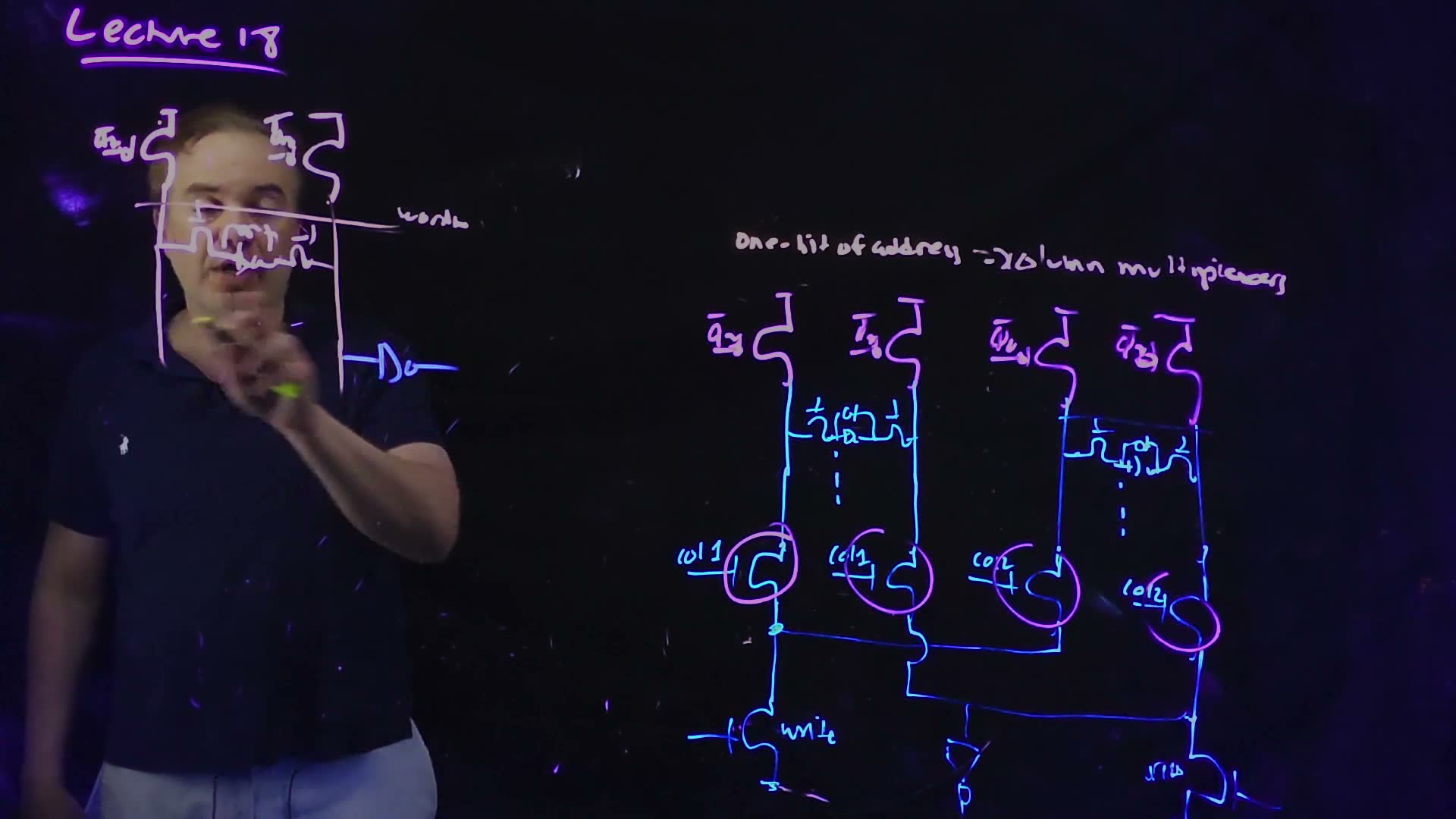
The column multiplexer (board, 31:55–37:18)
- One bit of address. “One-bit of address → column multiplexers” (board). With 128 columns and one column bit, two columns share one set of read and write circuits, and the word is 64 bits (32:44–33:12). In Chapter 18’s terms, .
- The circuit. Two columns, each with its own precharge PFETs and cells. Below the cells, an NFET in series with each bitline: both of column 1’s are gated by col 1, both of column 2’s by col 2. Below them the two bit lines join into one node, and the two lines into another.
- Shared circuits. One write device hangs from each joined node (§8’s one-device drivers), and the read inverter hangs from the joined node.
- The selects. col 1 and col 2 are the decoded column address: a full decode (§11) of the column bits, so exactly one is high.
- The second benefit (spoken, 49:56–51:24). The read and write circuits, and the sense amplifiers of §10, are much wider than a cell. With multiplexing they are shared among columns and need not fit in one column’s narrow pitch.
- The cost. “It adds this another device … into the stack” (36:35): the mux NFET is in series with the access NFET and the write device.
A 2:1 column multiplexer, redrawn from the board (Lecture18 @ 37:18). Two columns (bit₁, , bit₂, ), each with precharge PFETs on and a cell. Below the cells, a series NFET on each bitline, gated col 1 (column 1) and col 2 (column 2). bit₁ and bit₂ join (bit₁’s wire hops over , as on the board) and go to one write NFET, gate ; and join and go to the other, gate , with the read inverter on that shared node. The two write devices are §8’s one-device drivers.
The board (Lecture18 @ 37:18)
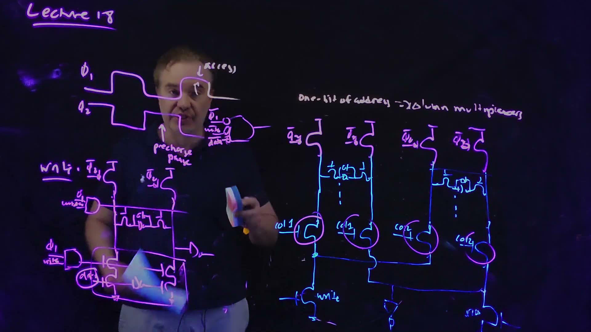
Fair copy of the board above (Lecture18 @ 37:18), mark for mark in its own layout. Black is the violet pen: the write board at the left, as at 31:37 (the one-device drivers are wiped, and the left driver’s AND stays with its output cut short), the multiplexer’s four precharge PFETs with their labels, and the rings round the four mux devices. Teal is the blue pen, the multiplexer itself: the bitlines and cells, the mux devices with col 1, col 1, col 2, col 2, the joined bitlines (column 1’s hops over the wire joining the two bits), the two write devices and the read inverter. The title, in the pale cream pen, is black. The write stacks’ middle, behind the papers in the lecturer’s hand here, is copied from 36:46. The right write device runs off the frame’s bottom edge.
What it costs added (§8’s divider, the example cell, for example: every write-path device 0.6 µm). With the two-high stack, the mux device takes from to . With the one-device driver, from to . That is why §8 removes a stack device before the multiplexer adds one.
A worked example. The board’s: 128 columns with one column bit give a 2:1 multiplexer and a 64-bit word. In Chapter 18’s terms, column bit. The cost: one more series device in the write path, as above.
The split itself, with its worked examples and the past final’s FN10-10, is Chapter 18’s (§10); this section adds the circuit it selects.
Traps.
- “The mux’s cost is a bigger decoder.” It costs the write path a series device. A 4:1 mux is still one device per path, but its selects need a 2-to-4 decode.
- “The detector sees the full bitline through the mux.” Through an NFET the shared node charges only to (an NFET pulling up, §3; the point of §10’s Check on the isolation devices), which can sit below §7’s switch point of : the skewed inverter would see every read as a fall. Behind an NFET mux the detector must switch below , or the shared node needs its own precharge, or the read path goes through PFETs or transmission gates.
- col 1, col 2 as address bits. They are the decoded one-hot lines; column bits make of them.
- Column bits as . They are : the multiplexer chooses words, not bits.
Check yourself 128 columns hold 16-bit words. What is the multiplexer's ratio, how many column bits are there, and how many select lines must the column decoder drive?
: an 8:1 multiplexer, 3 column bits, decoded into 8 one-hot select lines.
Check yourself (Two steps.) For example: the example cell with the one-device driver (0.6 µm). How much does VX rise when a 0.6 µm mux device is added, and how wide must the mux device be to keep VX at or below 0.35 VDD?
Without the mux, ; with it, 0.40 . For : . The access and driver take , leaving for the mux device: , so 2.6 µm, more than four times the driver’s width, and larger than the whole cell: the price of a series device.
10. Sense amplifiers: differential, regenerative, and their offset
You need
The cross-coupled pair (Chapter 13 §5). Two inverters in a loop have two stable states and a metastable one between them. Started slightly off balance, the loop runs away to the nearer stable state, faster the farther off balance it starts.
The bitline’s delay (§7). The cell discharges the bitline as one stage: to ; for a swing , (constant current near ). The example column: .
Switching energy (Chapter 6 §6). Restoring a node of capacitance by draws charge from the supply, so energy .
The question. The bitline falls slowly. Can the column decide which way the cell leans long before the bitline has fallen far, and what limits how early?
The clocked sense amplifier (board, 37:23–48:45)
- Differential. A sense amplifier compares bit with instead of comparing one line with a threshold. Noise that moves both lines together (coupling, supply bounce) cancels in the difference (37:23–39:20).
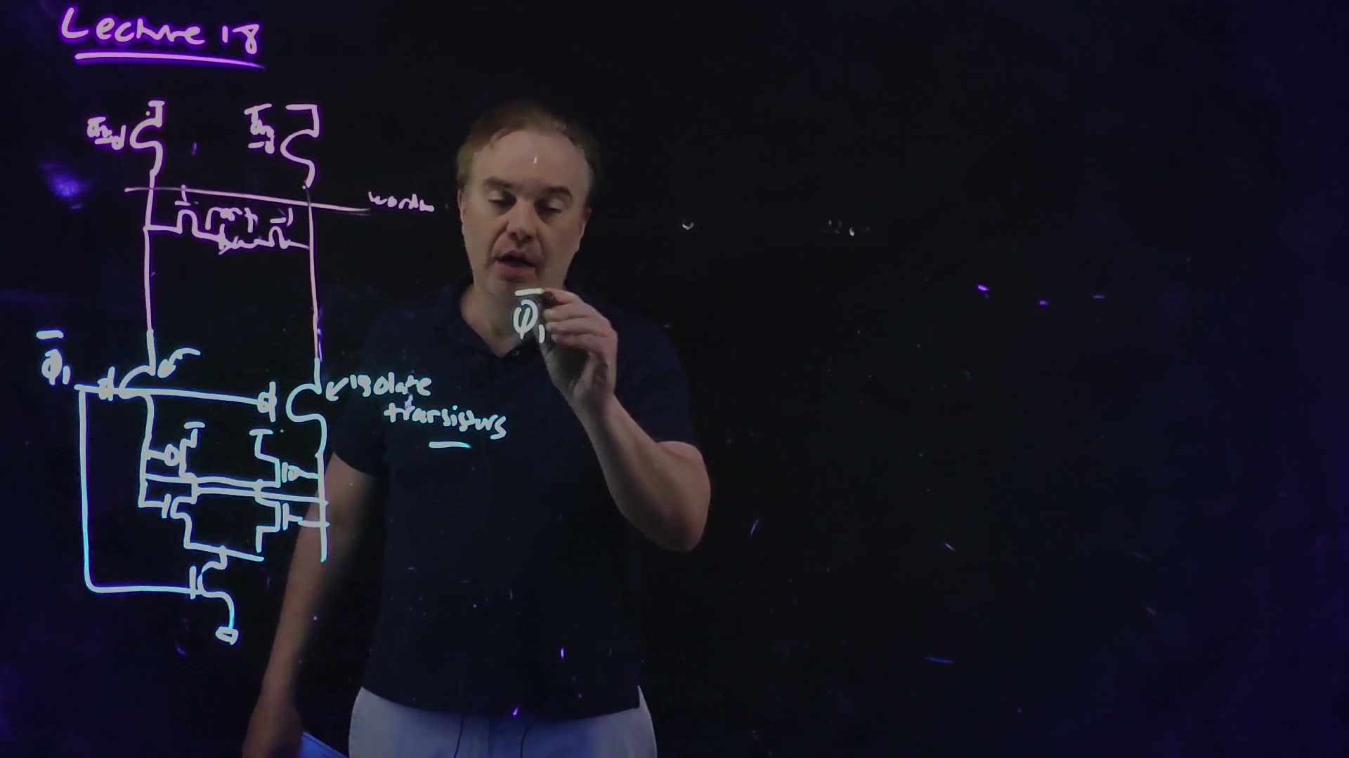
- The circuit. Below the cells, a PFET in series with each bitline, gates on : the isolation devices (“isolate transistors”). Below them, two cross-coupled inverters with sense nodes and , whose NFETs share a source; a tail NFET from that source to ground, gate also on (40:09–41:10).
- Don’t wait. “Waiting for this to get pulled all the way to ground is going to take a long time” (42:05). The amplifier needs only a small difference.
- During (). The isolation PFETs are on and the tail is off: the sense nodes follow the bitlines, and the cell’s small difference appears between and .
- At the end of (). The isolation PFETs turn off, cutting the sense nodes from the bitlines (which precharge once rises), and the tail turns on. The pair, started off balance by , regenerates to full rail: “that can happen very fast. It has nothing to do with gain bandwidth product” (46:30).
- The payoff. The bitlines swing only : a shorter access, and less charge to restore.
- The catch: offset. Mismatch between the pair’s devices (§5) makes the amplifier lean one way by itself, an input offset voltage. “These offsets can be quite large. They can be 50 to 100 millivolts” (48:15). The swing must exceed it, which erodes the advantage, and many SRAMs read single-ended again (47:37–48:45).
The clocked sense amplifier, redrawn from the board (Lecture18 @ 44:13; labels from 46:37 and 48:37). A column with precharge PFETs on , the word line and a cell. Below it, an isolation PFET in series with each bitline, gates on one wire; the sense nodes and (this guide’s names for the board’s x marks); two cross-coupled inverters between them, their NFETs meeting at a common node; a tail NFET from that node to ground, gate on .
The sense amplifier’s sequence added (from the board’s description, 43:28–46:57; a sketch). Rows , , WL, the bitlines and the sense nodes. While is high, bit sags by and the sense nodes follow. When falls, the bitlines are cut off and precharge, and the sense nodes regenerate: falls to 0 while holds . The dotted line at marks the swing the sag must pass before the amplifier fires.
Derive it from Chapter 6: the precharge draws of charge from .
A worked example added (the example column, for example: , fF, V).
Sensing 100 mV
- Time. The swing must exceed the offset; take mV, the board’s upper figure. , against 40 for the skewed inverter (§7) and 100 to . At 50 mV it would be .
- Energy. fJ per bitline per access, against 60 fJ for a swing of .
The board (Lecture18 @ 48:37)
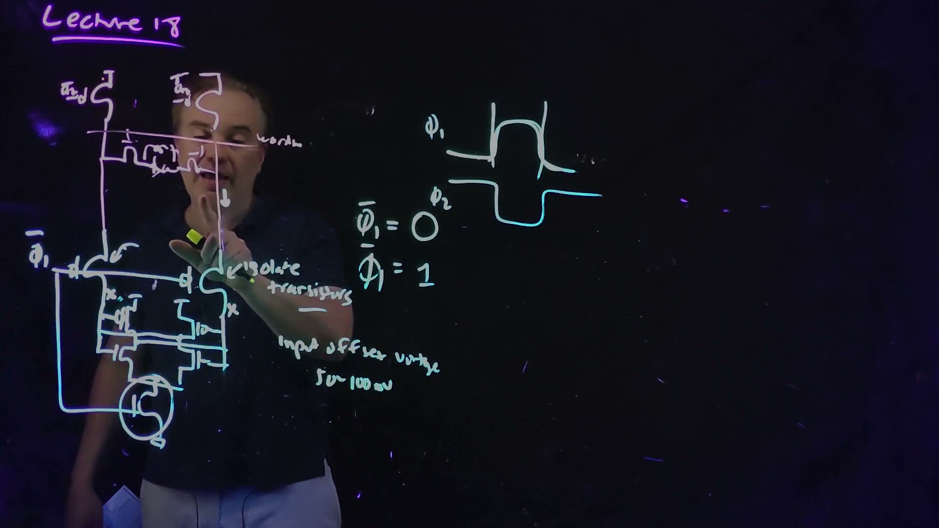
Fair copy of the board above (Lecture18 @ 48:37), mark for mark in its own layout. Black is the pale cream pen’s read column, drawn earlier: the precharge PFETs, “wordline”, the cell and the bitlines; “Lecture 18” is violet. Teal is the cyan pen, which adds the sense amplifier under the column and the notes beside it: the wire to the two isolation PFETs, the x marks on the sense nodes, the cross-coupled pair, the ringed tail NFET, the arrow on , the two clock states, the and waveforms with long vertical marks at the edges of the pulse, “input offset voltage” and “50∼100 mV”. The board draws each transistor as a channel bump beside a gate bar, a PFET with a small bubble, and writes the second with a capital . Nothing is restored: the lecturer’s hand washes out the right isolation device and the start of “isolate transistors”, and 47:52 has the same strokes clear; only “50∼100 mV” is new since then.
Traps.
- Firing before exceeds the offset. The amplifier resolves its own bias, not the cell’s data: a wrong read.
- Isolation devices left on during regeneration. The pair would have to swing the whole bitline, slowly, and fight the precharge.
- “A sense amplifier is a linear amplifier.” Its speed comes from positive feedback (regeneration), not from gain and bandwidth.
Check yourself Why are the isolation devices PFETs rather than NFETs?
They must pass the bitlines’ levels near to the sense nodes. A PFET passes a high level fully; an NFET would stop a threshold below (Chapter 10’s degraded high), right where the small signal lives.
Check yourself (Two steps.) For example: with a 75 mV offset on the example column, what is the earliest the amplifier may fire, and what restore energy does each bitline then cost?
Time: 15 of bitline sag. Energy: 9 fJ.
11. Decoders: AND gates, predecoding and clock qualification
You need
AND from NAND and NOR added (De Morgan, background). : a NOR of complements is an AND. So a NOR of NAND outputs is the AND of all their inputs: .
Pseudo-NMOS (Chapter 10 §10). An always-on PFET (gate grounded) pulls a line up; NFETs pull it down. The line is low whenever any NFET on it conducts: a NOR. Chapter 18’s PLA planes are built this way.
The question. How does the row decoder raise exactly one word line out of , and how is it built so that it is not one huge, slow gate per row?
Decoders (board, 51:24–53:38)
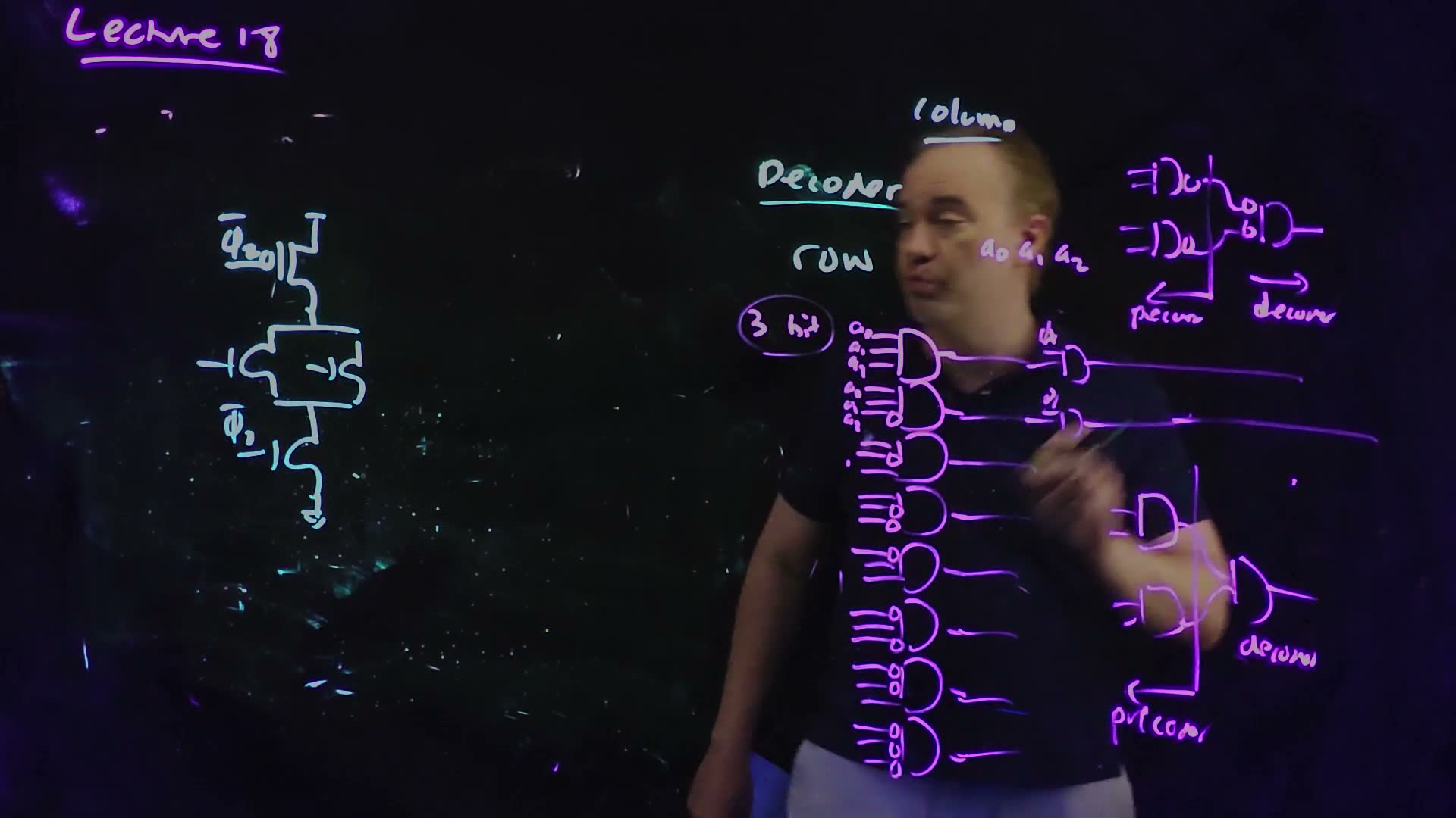
- One AND per row. “Decoders are nothing but a glorified set of AND gates” (51:24). For 3 bits, eight 3-input ANDs; each takes every address bit, true or complemented, so that exactly one AND is high for each address. The board bubbles the inputs in a binary count down the column.
- Clock qualification. Each AND’s output is ANDed with before it becomes a word line (§7).
- Two levels. A wide AND is slow, so split it. A predecoder ANDs small groups of address bits; the decoder ANDs one predecoded line from each group (53:04). In CMOS the natural form is NAND then NOR: the NOR of NAND outputs is the AND of everything (the board’s “precoder” and “decoder”).
A 3-bit decoder, redrawn from the board (Lecture18 @ 55:51). Eight 3-input ANDs, inputs , , with bubbles in a binary count; each output ANDed with (the board draws two of these; all eight are drawn here) into a word line labelled with its product, from to .
Two-level decoding, redrawn from the board (Lecture18 @ 55:51). (a) Two 2-input ANDs (the predecoder) into a 2-input AND (the decoder). (b) The CMOS form: two NANDs into a NOR. The vertical line separates the predecoder from the decoder.
Counting a predecoded decoder
An 8-bit decoder with 2-bit predecoding (added)
- Groups. Split the 8 address bits into groups of 2.
- Lines per group. Each group of 2 bits is fully decoded into one-hot lines: predecoded lines in all.
- Decoders. Each of the word lines needs one line from each group: a 4-input gate.
- Fan-out. A given line of one group is used by every row whose bits in that group match it: decoders.
Derive the counts each time from the picture: groups, lines per group, one line per group per decoder.
A decoder driving a ROM
The same full decoder, driving a grid of pull-down devices on pseudo-NMOS columns, is a ROM added (a bridge to a past final, FN12-10d). Each address raises one row; a device at a crossing pulls its column low when its row is selected; a column with no device on the selected row stays high. Read it row by row.
A small ROM added: a 2-to-4 decoder (four 2-input ANDs on , ) drives four rows. Two pseudo-NMOS columns , each have a PFET with its gate grounded at the top. NFETs from a column to ground, gated by a row, sit at row –, row –, row – and row –; row has none.
Reading the ROM, row by row (added)
- . Row is selected; it has a device on only: .
- . Row has no device: .
- . Row has devices on both: .
- . Row has a device on : .
The board (Lecture18 @ 55:51)
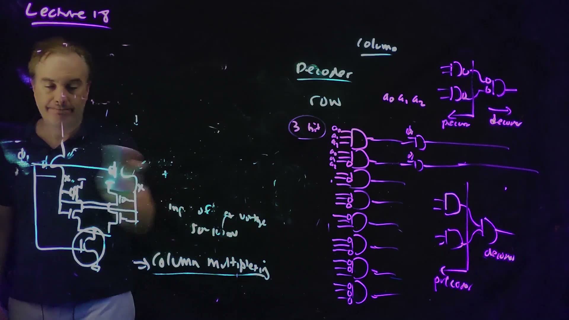
Fair copy of the board above (Lecture18 @ 55:51), mark for mark in its own layout. Black is the violet pen: “Lecture 18”, “3 bit” with its ring, , and the decoders: eight three-input ANDs with bubbles on the complemented inputs, the first two ANDed with into long word lines, two NANDs into an AND with bubbled inputs, and two ANDs into an AND, each pair split by a line into “precoder” and “decoder”. Teal is the cyan pen: the titles “column”, “Decoder” and “row”, and at the left what remains of the sense-amplifier board as it is wiped, with “⇒ Column multiplexing”. The wipe has taken the read column, “isolate transistors” and the clock states; the copy keeps what remains, down to the letters left of “input offset voltage” and “50∼100 mV” and a few short pieces of the column. The right isolation device’s gate and the right PFET’s top bar show through the lecturer’s hand and are copied as they stand at 55:08. “precoder” is the board’s shortening of “predecoder”, the word the lecture uses. The tiny input labels the board writes beside the first two ANDs are left out: typeset, they would overlap.
Traps.
- The fan-out of a predecoded line as all decoders. Each decoder takes one line per group, so a line feeds only the rows that match it: .
- Leaving out the clock qualification. While the address changes, two decoder outputs can be high for a moment; without two word lines could rise together.
- Reading a ROM device as a 1. A device pulls its column low.
Check yourself A 6-bit decoder uses 3-bit predecoding. How many predecoded lines are there, how many inputs does each word-line gate have, and how many gates does each line feed?
groups of lines: 16 lines. One line per group: 2 inputs. Fan-out 8.
Check yourself (Two steps.) In the ROM figure, which address gives an all-ones output word, and why? Which gives all zeros?
Address 01: its row has no device, so nothing pulls either column low and both PFETs hold them high. All zeros: address 10, whose row has a device on both columns.
12. The race-based NOR
You need
Precharge and evaluate; the race (Chapter 11 §4–§5). A dynamic gate’s node is precharged high while its clock is low and can only fall while its clock is high (its foot NFET on). If its output drives an NFET of a second dynamic gate that evaluates at the same time, the second gate sees a high input at the start of every evaluation, even when the first node is about to fall: it can discharge by mistake. That is the race; domino logic puts an inverter between the stages to avoid it.
The half latch (Chapter 11 §8). A weak PFET from to a dynamic node, gated by the inverter after it, holds a high node high against leakage and noise.
The two phases with a gap (§6). Precharge while is high, access while is high, and a non-overlap time from falling to rising.
A dynamic stage’s gain (Chapter 12 §2). On its evaluation edge a footed stage pulls down through its input NFET and its foot in series: gain with . An inverter’s rising edge is driven by its PFET, , as strong as an NFET of : gain .
The question. The word line must rise for one row only, and only in the access phase. Can the decoder’s last gate and the clock qualification be one fast dynamic gate pair, and what does the clock have to do to make that safe?
The circuit
The race-based NOR (board, 56:10–57:02)
- Stage 1: the decoder’s NOR. A dynamic NOR of the row’s predecoded lines (two on the board): a PFET from to node , gate , so precharges while is high; the input NFETs in parallel; a foot NFET, gate , so the gate evaluates as soon as falls. (“This is phi one bar … excuse me, phi two bar”, 56:10.) stays high only on the selected row, the one whose inputs are all low; on every other row some input is high and falls.
- Stage 2: the clock qualification. A second dynamic stage: a PFET from to node , gate (precharge while is low); an NFET gated by ; a foot NFET gated by , which the board rings: “clock qualification”. falls only if is high while is high.
- The word line. drives an inverter whose output is the word line, with a half latch (a PFET from to , gate on the word line) to hold high on the unselected rows.
- The board’s stage-2 device. The board draws stage 2’s top device without a bubble. It must be a PFET: an NFET there would conduct together with the foot and short the supply to ground. The redraw draws the bubble.
The race-based NOR, redrawn from the board (Lecture18 @ 58:46; stage 1 as uncovered at 56:46). Stage 1: a dynamic NOR of the predecoded lines , , precharged and footed on , node . Stage 2: precharged by a PFET on (bubble drawn; the board omits it), an NFET gated by , and the foot, the clock qualification; node . An inverter from drives the word line WL, with a half-latch PFET back to . The labels , , and are this guide’s.
The board (Lecture18 @ 58:46)
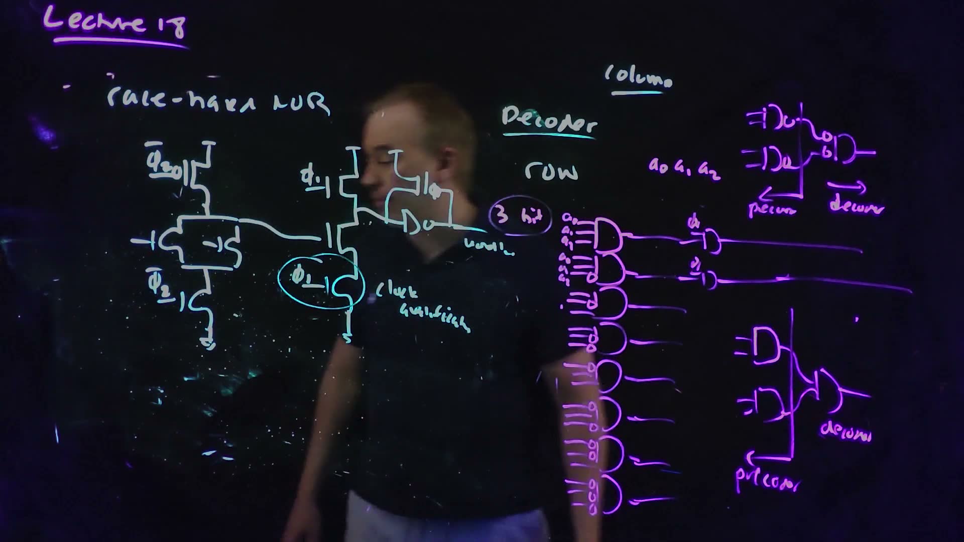
Fair copy of the board above (Lecture18 @ 58:46), mark for mark in its own layout, on the 55:51 copy’s coordinates; its decoder half is that copy’s, unchanged. Teal is the cyan pen: “race-based NOR” and its circuit, and the titles “column”, “Decoder” and “row”. Black is the violet pen’s decoders and “Lecture 18”, and three short pieces of the wiped read column. Stage 1: a PFET on (its bubble is the small o after the label), two input NFETs in parallel and a foot on . Stage 2: the device on is drawn without a bubble, as on the board; it is a PFET, since an NFET there would conduct with the foot and short the rails. Its NFET takes stage 1’s node, and its foot on is ringed: “clock qualification”. The node drives an inverter to “wordline”, with a half-latch PFET whose gate is the inverter’s output. Nothing is restored: the lecturer stands in front of the half latch and the inverter, which show through, and 58:01 has the same strokes. The tiny input labels beside the first two ANDs are left out, as in the 55:51 copy.
The race, and the clock that removes it
Stage 1’s node drives stage 2’s NFET directly: a precharged-high node into a dynamic gate, Chapter 11’s race. “This is often called a race-based NOR because there’s an inherent race condition here” (57:49).
Edge by edge (board 57:19–57:49; the timing is added)
- Precharge ( high). is high on every row; is high (its PFET is on while is low); every word line is low.
- falls. Stage 1’s foot turns on. On the unselected rows starts to fall, taking a time . On the selected row stays high.
- rises, later. Stage 2’s foot turns on. On the selected row is high, so falls and the word line rises: the access begins.
- The race. On an unselected row, if is still high when rises, stage 2 sees a high input and starts to discharge : a glitch on a word line that must stay low, and two rows accessed at once. The fix is the clock: “I can twiddle the phi one, phi two bar relative to the phi one to ensure that this guy evaluates before this guy evaluates … I get rid of the race condition” (57:19–57:49). Make longer than stage 1’s evaluation.
- falls. Stage 2’s PFET turns on, precharges high and the word line falls (on the board’s circuit).
The race-based NOR’s timing added (a sketch, from the board’s spoken sequence, 57:19–57:49). falls at and rises later. on an unselected row falls within , shorter than ; on the selected row (dashed) it stays high. on the selected row falls just after rises and is restored when falls; the word line follows, inverted. On an unselected row stays high; the dotted dip marked ✗ is what would happen if were still high when rose.
Derive it from the edge-by-edge picture: an unselected row’s must be low before stage 2’s foot opens. Precharging stage 1 on rather than (§6) is what makes the gap available.
Two remarks. First, a variant: if stage 2’s PFET is gated by the line instead of (as on the 2017 final’s circuit, FN17-6), is precharged only while is high, so the selected word line stays high from rising until rises, through the second gap. Both versions work; the board’s word line falls with . Second, the clocked design is not the only one: SRAMs can be self-timed with a replica column that triggers the end of the access, “but they’re far more complex” (54:20–55:21; Chapter 18’s replica rows are the same idea).
The decode path’s delay
The critical edges run through the predecoder and the race NOR on the unselected rows (they must finish before ), and through stage 2 and the word-line driver on the selected row (after ). Add them as Chapter 8 does, one gain per stage.
A decode path for a 64-row array added (for example; the shape of the course’s design-project decoder with this guide’s sizes, in µm). I: a domino NOR2 predecoder (precharge PFET 4 on , inputs and foot 8). II: its inverter (PFET 30, NFET 5), each output feeding 16 race NORs. III: the race NOR3 (precharge PFET 2 on , inputs and foot 3). IV: stage 2 (PFET 6 on , NFET 12, foot 12 on ). V: the word-line driver (PFET 40, NFET 6) into . Under each stage, its gain: 2.92, 1.07, 2.67, 2.56, 0.81. The dashed line marks the edge: stages I–III before it, IV–V after.
A worked example added (for example: the path in the figure, fF/µm; the word line has 20 fF of wire and 64 cells with 0.3 µm access devices).
The example decode path, stage by stage
- I, the predecoder falls. Drive: input 8 in series with foot 8, , normalized input 12. Load: the inverter, . Gain .
- II, the predecoded line rises. Driven by its PFET of 30, normalized input . Load: 16 race NOR inputs of 3, . Gain .
- III, the unselected race NORs fall. Input 3 in series with foot 3, , normalized input 4.5. Load: stage 2’s NFET, 12. Gain .
- IV, stage 2 falls on the selected row. 12 in series with 12, , normalized input 18. Load: the driver, . Gain .
- V, the word line rises. The word line’s load: two access gates per cell, fF, which is 48.4 µm. Driven by a PFET of 40, normalized input 60. Gain .
- Add. . Before (stages I–III, the minimum ): . After (IV–V): .
Derive it from the cell: two access gates per cell. Memorize the factor of 2.
On a past final (FN10-5a). The 2010 final asks for this kind of path, with its own sizes, for a word line of 256 cells with 1 µm access transistors and 100 fF of wire. Its answer key writes the word-line load as “100fF + 256(2fF)”, one access device per cell (612 fF). A 6T cell puts two access gates on the word line: fF. Driven by the paper’s 100 µm PFET, the last stage’s gain is , not the key’s 2.04, and the path comes to , not . The memory practice page (FM1) solves the question.
On a past final (FN17-6). The 2017 final prints a four-row version of this decoder with one column. Its scan hides the bars on in the W0 and W2 decoders, under their drain wires. Read W0 = NOR(, ), W1 = NOR(, ), W2 = NOR(, ) and W3 = NOR(, ). W1’s and W3’s labels are clear, and with them this is the only reading in which every address selects exactly one row. FM1 traces the waveforms.
Traps.
- One access device per cell on the word line. The example path would then see fF and a last-stage gain of 0.49 instead of 0.81: the 2010 key’s slip.
- Adding the stages of different rows as if they were one gate. The path mixes edges: the unselected rows’ race NORs before , the selected row’s stage 2 and driver after it. Each stage’s critical edge is the one that must finish for the access to work.
- Stage 1 precharged on . Then it could evaluate only from rising, together with stage 2: no gap to win the race.
Check yourself What goes wrong on an unselected row if tNO = 0?
Stage 2’s foot opens while that row’s is still high, so starts to discharge before falls: the unselected word line glitches up, and two rows may be accessed at once, which corrupts a read and can write the wrong cell.
Check yourself (Two steps.) For example: the array of the worked example grows to 128 columns (64 rows still). What are the new word-line load, the last stage's gain, the path's total, and the minimum tNO?
Load: 173.6 fF, 86.8 µm. Gain: 1.45. Total: 10.65 (summed from the unrounded gains; the rounded terms add to 10.66). The minimum is unchanged, 6.65 : stages I–III do not see the word line.
Check yourself In the variant whose stage-2 PFET is gated by φ̄2, when does the selected word line fall?
When rises: only then does fall and turn the PFET on, restoring high. Through the gap after falls, floats low and the word line stays high.
13. Putting it together: the access time
You need
The bitline (§7): to , the access and pull-down NFETs in series; a smaller swing takes . The example column: 100 to , 40 with a skewed inverter at .
Sensing (§10): a sense amplifier fires once the swing exceeds its offset, 50–100 mV; 20 at 100 mV on the example column.
The decode path (§12): one gain per stage, added; the example path is 10.0 .
The question added. How long is one read, from the address to the data, and does it fit in a processor’s cycle?
The access time of the example array (added)
- Add the parts. A read is the decode path, then the bitline’s swing, then the detector. With the skewed inverter: . With a sense amplifier at 100 mV: (the amplifier’s own regeneration, a few , is left out).
- Convert. The course’s finals take FO4 ≈ 3 (FN10 states it). Single-ended: FO4. Sensed: FO4.
- Against a cycle. A processor cycle of 12–15 FO4 is 36–45 . The single-ended array needs more than a cycle; the sensed one fits.
- The bitline dominates. In both, the bitline is two to four times the decode: optimize it first.
The example array’s access time added, computed from §7, §10 and §12 (for example). Two bars on one axis in : SE, single-ended with the skewed inverter: decode 10.0 (hatched) and bitline 40.0, total 50.0; SA, with a sense amplifier at 100 mV: decode 10.0 and bitline 20.0, total 30.0. Dotted lines at 36 and 45 mark cycles of 12 and 15 FO4 at 3 per FO4.
Derive it by adding the parts; memorize that the bitline usually dominates.
The remedies, each from this chapter or the last:
- Sense a small swing (§10): the bitline term falls in proportion to .
- Shorter bitlines: fewer rows per bank (Chapter 18’s organization); the bitline term falls in proportion to the rows.
- Self-timing (§12): end the access when a replica column says the data is ready, not at a fixed clock edge.
- Pipelining (Chapter 14): spread the access over two cycles, with the decode in one and the bitline in the next.
Traps.
- Optimizing the decoder first. In these numbers the bitline is the larger term.
- Mixing FO4 conventions. State the conversion you use; FN10 gives FO4 ≈ 3 .
Check yourself (Two steps.) For example: halve the example column's rows, so its bitline is 60 fF. What is the new single-ended access time, in τinv and in FO4?
Bitline to : ; with the skewed inverter, . Access: 30.0 , 10.0 FO4: halving the rows does what the sense amplifier did. (The decode loses a predecode bit too, which this estimate ignores.)
Check yourself Which single change to the example array helps the access time most: halving the decode path's delay, or sensing 50 mV instead of 100 mV?
Halving the decode saves . Sensing 50 mV saves on the sensed array: the bitline term is the larger lever.
On the exam
Three past finals test this chapter, about 57 points in all. The memory practice page (FM1) solves them; the 2010 and 2017 decoders are the course’s design-project decoder of §12.
| Part | Points | What it asks | Sections |
|---|---|---|---|
| FN10-5a | 10 | the decode path’s delay through a domino predecoder and a race-based NOR, in (the key undercounts the word line: §12) | §12, §11 |
| FN10-5b | 10 | the bitline’s delay to through the cell’s two NFETs | §7 |
| FN10-5c | 6 | the access time in FO4, why it is a problem in a 12–15 FO4 cycle, and one remedy | §13, §10 |
| FN10-10b | 6 | the column-multiplexing bits for a 4k × 16 memory built as 256 × 256 | Chapter 18 §10; the multiplexer it selects, §9 |
| FN17-6a | about 8 | the decoder’s and the column’s waveforms over write and read cycles | §12, §8, §7 |
| FN17-6b | 8 | the clock condition that removes the race | §12 |
| FN12-10d | 9 | a ROM: a full decoder into pseudo-NMOS columns, read row by row | §11 |
At the finals’ pace of 0.7–0.9 minutes a point, FN10-5 is an 18–23 minute question.
Memorize.
- The cell’s strength order, pull-down > access > PFET, and both ratios with their reasons: access about 3× the PFET’s strength (1.5× its width, the PFET half as strong per width); pull-down 1.5–2× the access device.
- The read and write sequences: precharge both bitlines, raise the word line, then one bitline falls (read) or is pulled low (write).
- The butterfly: read lifts both lows and shrinks both lobes; a write caps one side and closes the old state’s lobe. The static noise margin is the side of the largest square in the smaller read lobe.
- Precharge on , access on ; the word line is the AND of and the decode.
- The board’s write column: data on the bit side, so a read through the inverter on returns the complement of the data written.
- Two access gates per cell on the word line.
- A sense amplifier’s offset: 50–100 mV.
- The race in words: an unselected row’s first stage must fall before opens the second stage’s foot.
Derive (with the path).
- The two dividers (§2, §3): from against ; from against .
- The bitline (§7): series width, normalized input , load ; a smaller swing in proportion.
- The address split (Chapter 18 §10): .
- Predecode counts (§11): groups of lines; fan-out .
- The race condition (§12): of the stages between falling and rising.
- The decode path and the access time (§12, §13): one gain per stage, the word line with two gates per cell; add the bitline; FO4 ≈ 3 where the paper says so.
Method cards. The memory families (the decode path’s delay; the bitline and the access time; address bits; decoder and column waveforms; ROM tables) have their playbook cards: SRAM access path, memory addressing and ROM decoders and dynamic row decoders.
The lecture’s boards
The boards of Lectures 17 and 18 used in this chapter (24 frames)