7. Delay models and static CMOS gates
Lecture 6 described how an inverter switches: a curved trajectory across the I–V curves, a 50% delay, a slew. That picture is accurate but far too slow to use for every gate on a chip. Lecture 7 replaces it with the model designers actually use for quick estimates: every transistor is a “resistance” that shrinks with its width, every gate input is a capacitance that grows with its width, and delay is one times the other. The lecture shows how to measure the two numbers for a technology, then builds the logic gates beyond the inverter (static CMOS: NOR, NAND, AOI), and finally uses the model to compare them. The comparison gives the lecture’s last and most important idea: a NAND or NOR is slower than an inverter of the same strength by a fixed factor, its logical effort.
After this chapter you can:
- explain the simplified delay model and why its “resistance” is really a constant of proportionality between load and delay;
- use in fF/µm and , in kΩ·µm to compute the delay of any transistor driving any load;
- describe the two fan-out-of-four simulations that measure and , and say why drain capacitance must be zeroed in one of them;
- state what makes a gate static CMOS, build complementary NOR, NAND and AOI gates as duals, and check their truth tables;
- explain pin swapping, why tall stacks are avoided, and how a static gate can be non-complementary;
- derive , size a stack for equal drive, and find the logical effort of NAND (4/3) and NOR (5/3);
- write a gate’s delay as its gain times .
Boxes and equations marked board were written in the lecture. Parts marked added are explanations or examples this guide adds.
Before you start
You need these ideas from earlier chapters. Each is restated here.
- Gate capacitance (Chapters 4 and 5). A transistor’s gate is a capacitor of area with per unit area, so .
- Current grows with width (Chapter 4). Every I–V model has . Twice the width carries twice the current, so it charges a load in half the time.
- PFETs are weaker (Chapter 5). Holes are slower than electrons, so a PFET delivers about half the current of an NFET of the same width. An inverter’s PFET is made twice as wide ( against ) for equal rise and fall.
- FO1 and FO4 (Chapter 5). The delay of an inverter driving one copy of itself (fan-out of one), or four copies (fan-out of four).
- Delay and slew (Chapter 6). Delay is measured from the input’s 50% point to the output’s: for a falling output, for a rising one. A saturated ramp is a waveform that is flat, ramps linearly, and is flat again.
Notation. and are the NFET and PFET widths. A sizing written “16/8” means a PFET 16 µm wide and an NFET 8 µm wide, as on the lecture’s boards; “4(16/8)” means four times that, 64/32. The board writes and ; this chapter writes them the same way. is the FO1 delay (Section 7).
1. From trajectories to a simple delay model
The idea. Treat the pull-up and pull-down as a switch with a resistor, so that every delay is a “resistance” times the capacitance being driven.
The trajectory, once more
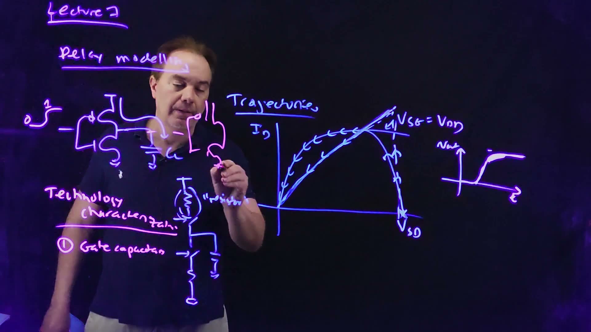
The lecture starts where Lecture 6 ended (00:25). An inverter’s input switches from to 0, and its PFET charges the load. On the PFET’s I–V curves the operating point rises quickly to the full-overdrive curve, , then rides that curve down (01:10). The output rises almost linearly at first, then slows into a tail as the PFET leaves saturation for triode (01:41). Lecture 6 called this the trajectory.
The simplified picture
Since the 1980s, designers have used a much simpler picture (02:09) board:
- each pull-up and pull-down network is a switch in series with a resistor;
- switching the input closes one switch, and the load charges (or discharges) through that resistor;
- on the I–V plane, the curved trajectory becomes a straight line: an immediate jump up, then charging along a resistor’s line (02:39).
A constant of proportionality, not a resistor
The lecturer is careful about the word (03:09). The “resistor” is not a real resistor in the circuit. It is a constant of proportionality between capacitance and delay, measured for each technology:
The delay is linear in the load, and the constant has the units of resistance (03:29). Since it is measured as delay ÷ capacitance, it already contains whatever factors the real waveform has.
Units. added . With in kΩ and in fF, the delay comes out in picoseconds directly.
Common mistakes.
- Multiplying by . added For a real resistor and capacitor, the 50% point comes at . Here is defined as measured delay ÷ load, so already is the 50% delay; multiplying again by 0.69 gets the measurement wrong.
- Thinking the model describes the waveform. It predicts one number, the delay, and nothing about the shape.
2. Characterizing a technology: gate capacitance and resistance
The idea. Two numbers per technology are enough: the gate capacitance per micron of width, and the “resistance” times micron of width for each kind of transistor.
Number one: gate capacitance per micron
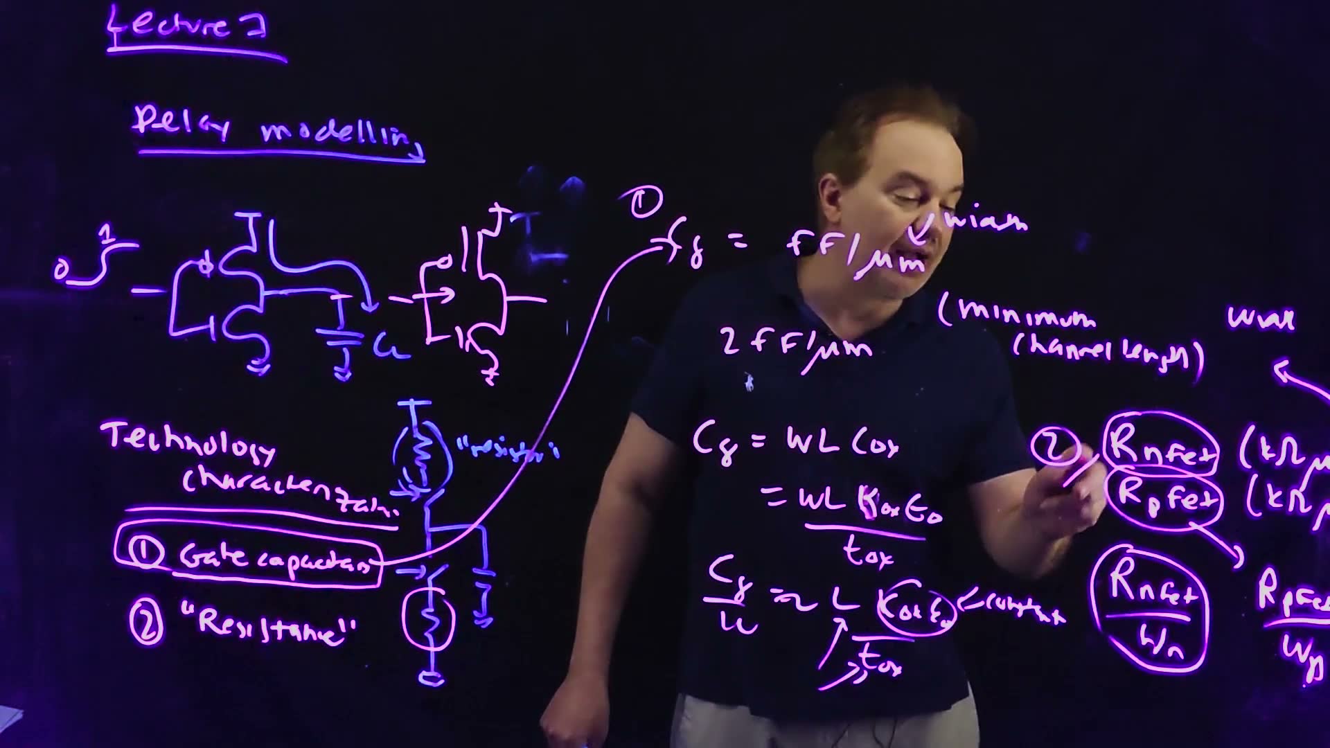
When one inverter drives another, what capacitance does it see looking into the second one’s input (04:15)? The lecture characterizes it as femtofarads per micron of device width, in fF/µm, for a minimum-length device, because almost every logic transistor is minimum length (05:03–05:30) board.
- The number is about 2 fF/µm board, essentially the same for NFETs and PFETs (05:58).
- It has stayed near 2 fF/µm for many technology generations. Recently it has drifted a little, and the problem set’s 90 nm technology gives a slightly different value (06:00).
Why it hardly changes (06:15–07:32):
Gate capacitance per micron of width (board, 06:15–07:32)
- The gate is a capacitor of area board: .
- With the oxide capacitance written out board: . (The lecturer starts to say “epsilon ox” and corrects himself to , the oxide’s dielectric constant.)
- Divide by the width board: . The factor is a constant.
- Under Dennard scaling (Chapter 4), and both shrink by the same factor . Their ratio doesn’t change, so neither does (07:06).
Worked example. added Chapter 4’s device, and :
- .
- Convert: , so .
- : close to the lecture’s 2 fF/µm.
- Scale by : , . doubles and halves, so is still 1.60 fF/µm.
Loads as widths. added Since every gate input is per micron, a load can be written as an equivalent gate width, . At 2 fF/µm, a 50 fF load “is” 25 µm of gate. Past exams use this often.
Number two: resistance times micron
The second number is the “resistance” of each kind of transistor, in kΩ·µm, where the micron is again the channel width (08:05) board. There is one value for the NFET and one for the PFET:
- divide by the actual width to get that device’s resistance: and (08:24) board;
- multiply by the load to get the delay of discharging (NFET) or charging (PFET) it (08:49).
A PFET has half the current drive of an NFET, so a characterized technology should show (09:20).
Worked example. added A technology with and ; an inverter with an 8 µm PFET and a 4 µm NFET drives 20 fF.
- NFET: , so .
- PFET: , so .
- Equal: the 2:1 width ratio exactly cancels the 2:1 resistance ratio. That is why inverters are sized .
Check yourself An NFET 2 µm wide, in a technology with Rnfet = 2.5 kΩ·µm and Cg = 2 fF/µm, discharges a load equal to 12 µm of gate. What is the delay?
The load is . The NFET’s resistance is . Delay .
3. Measuring the two numbers in simulation
The idea. Both numbers come from fan-out-of-four simulations with the technology’s SPICE models: first match a plain capacitor to a gate’s load to find , then time an inverter driving a known gate load to find .
When you get a new technology’s models, you run a few circuit simulations to find , and (09:20). The lecture describes the two set-ups you will build in problem set 3, for its 90 nm technology (10:01, 25:26).
Bench 1: gate capacitance
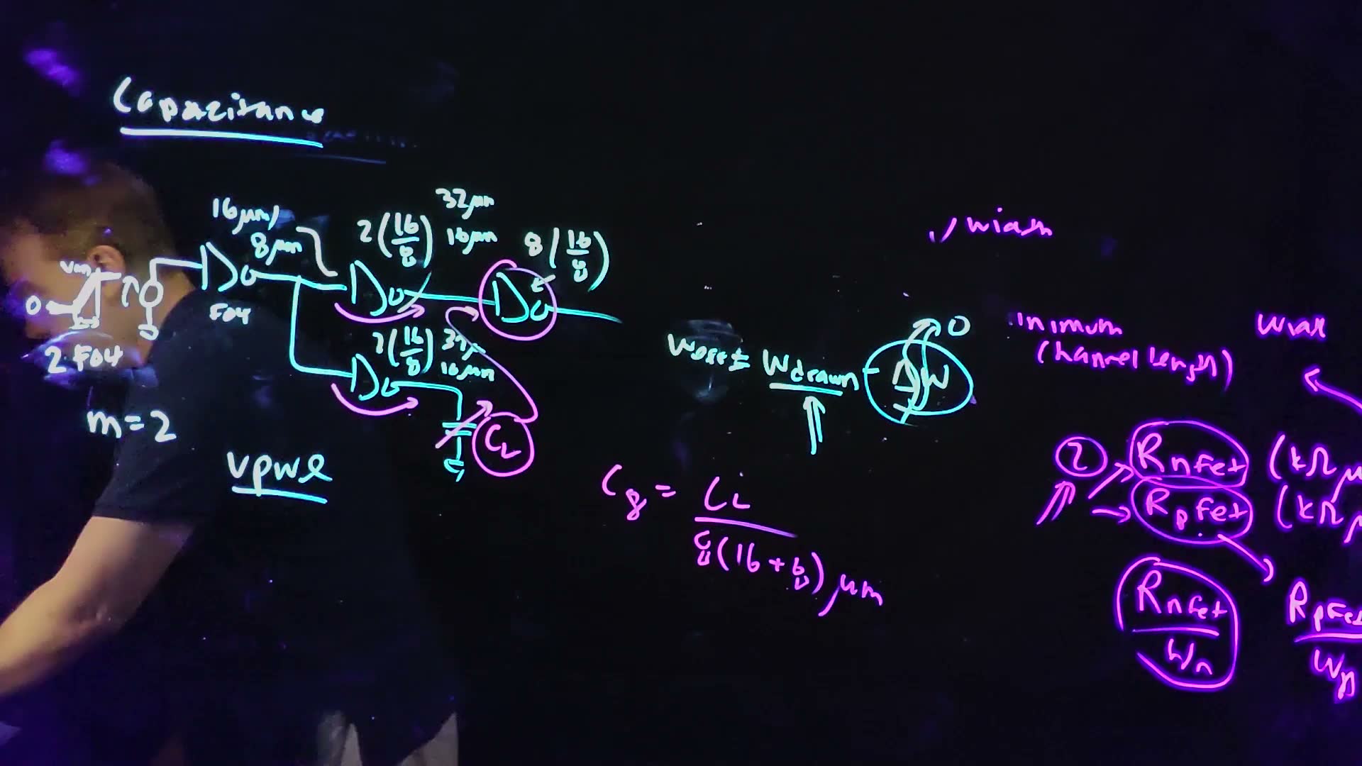
The circuit (10:49–14:23) board:
- A first inverter of 16/8. The lecturer picks “something relatively beefy” on purpose (11:03). The width a transistor really has is the drawn width minus a correction, board, and for very narrow devices matters. Wide devices make it negligible (11:30–12:32). (He says “let me just make it 10 by 8” at 12:32; the board, and his words before and after, say 16 by 8.)
- It drives two inverters of 2(16/8): a 32 µm PFET and a 16 µm NFET each. Together they are four times its own size, a fan-out of four (12:32). In the schematic you can type 32 and 16, or type 16 and 8 and set the multiplier , two devices in parallel (13:26).
- The upper 2(16/8) drives an inverter of 8(16/8), four times its size: fan-out of four again (14:03).
- The lower 2(16/8) drives a plain capacitor .
The input is a saturated ramp from 0 to , entered with the VPWL source (14:32). Its slew time is set to about twice the FO4 delay, which you measure separately: that is roughly the slew of a real gate loaded at fan-out of four (15:06–15:27). The ramp is still too abrupt to be realistic, so the first inverter’s job is to clean it up into a genuine FO4 waveform (16:00).
The measurement (16:32–17:51). Vary until the two 2(16/8) inverters have equal delays, rising or falling, it doesn’t matter. Then is the input capacitance of the 8(16/8) inverter, whose gates total board:
Bench 2: resistance
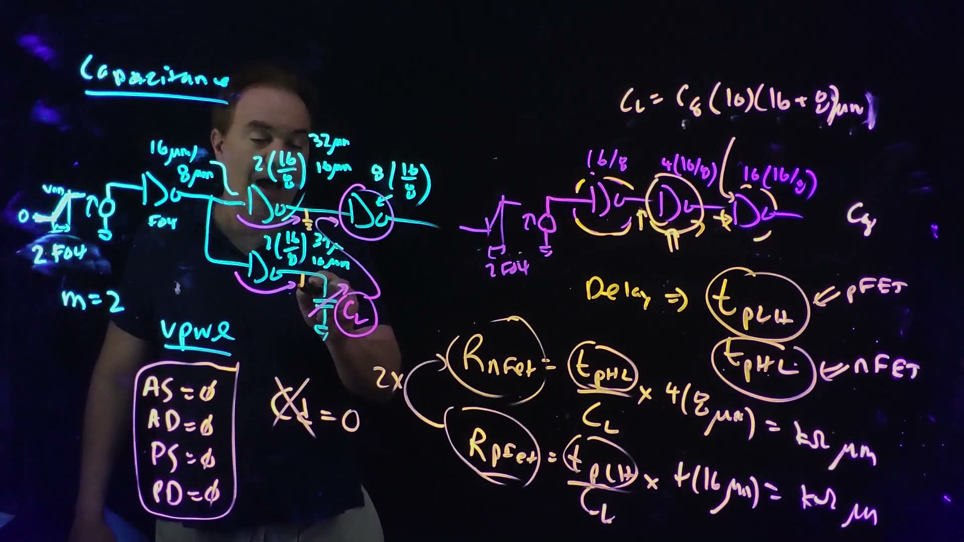
The circuit (18:36) board: three inverters in a row, 16/8, 4(16/8) and 16(16/8), each at fan-out of four, driven by the same kind of ramp. The first cleans up the waveform; the last provides a realistic load; the one being measured is the middle one (19:09).
Measure its two delays (19:38–20:06) board: characterizes the PFET (pull-up), the NFET (pull-down).
R from the middle inverter (board, 20:06–22:23)
- The load is the last inverter’s input board: , using the from bench 1.
- Delay ÷ load gives the NFET’s resistance in kΩ; multiply by its width, board: , in kΩ·µm.
- The same for the PFET, width board: .
- The inverter is sized 2:1 for equal pull-up and pull-down, so the two delays should be about equal, and then comes out twice board (21:40–22:23).
Zero the drain capacitance
This model’s only load is gate capacitance (22:30). Lecture 5 showed how important drain capacitance is, but the quick sizing methods that follow ignore it, and full circuit simulation corrects for it later (22:56). So the characterization must ignore it too.
- In Virtuoso’s instance properties, each transistor has four parameters describing its diffusions: AS and AD, the source and drain areas, and PS and PD, their perimeters (23:14). Setting all four to zero removes the junction capacitance, the main part of the drain capacitance board.
- It matters in bench 2: the middle inverter’s own drain capacitance would add to its load and make come out too large (24:56).
- It doesn’t matter in bench 1: both 2(16/8) inverters have the same drain capacitance, so it affects both delays equally and the match happens at the same (24:30).
Try both benches. Slide the capacitor until the two delays match, read off , and watch the resistances underneath. Then switch the drain capacitance back on.
What to notice.
- Away from the match, the you read is wrong, and both resistances inherit the error: bench 2 divides by a load computed from your .
- Turn the drain caps on: the crossing in bench 1 doesn’t move, but bench 2’s delays grow and both resistances come out 12.5% too large in Technology 1.
- Bench 2’s delay is an FO4 delay, and in this model it equals exactly (Section 7). added
Worked example. added Illustrative numbers, the widget’s Technology 1.
- Bench 1 matches at : .
- Bench 2’s load: .
- Bench 2 measures .
- .
- : twice , as expected.
- Had the drain caps been left in, with (Chapter 5’s ): the middle inverter adds , the delay becomes , and the extraction gives , 12.5% too high.
Common mistakes.
- Dividing by the wrong width. Bench 1 divides by the receiving inverter’s total gate width, . Bench 2 multiplies by the measured inverter’s NFET (or PFET) width, (or ).
- Using for the NFET. A falling output is the NFET’s job: goes with .
- Forgetting to zero AS, AD, PS, PD in bench 2.
Check yourself In bench 1 the two delays match at CL = 150 fF. What is Cg? Bench 2 then gives tpHL = 30 ps. What is Rnfet?
. Bench 2’s load is , so . (HW3-1 asks exactly this, with simulated numbers.)
Check yourself Why does bench 1 still give the right Cg if you forget to zero the drain capacitance, while bench 2 doesn't give the right R?
In bench 1 two identical inverters are compared, and each carries the same drain capacitance, so it adds the same delay to both and cancels in the comparison. In bench 2 the measured delay is divided by the gate load alone, so any drain capacitance is wrongly charged to the transistor’s resistance.
4. Static CMOS gates
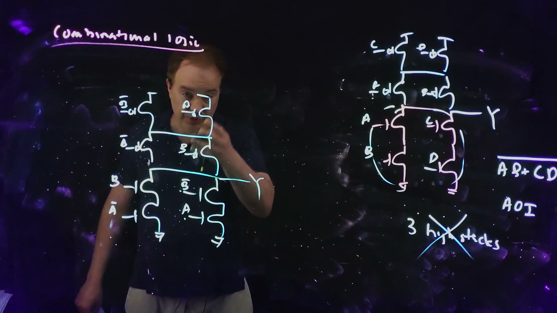
The idea. A static CMOS gate has a pull-up network of PFETs and a pull-down network of NFETs, and for any settled inputs exactly one of them is on. Making the two networks duals of each other guarantees it.
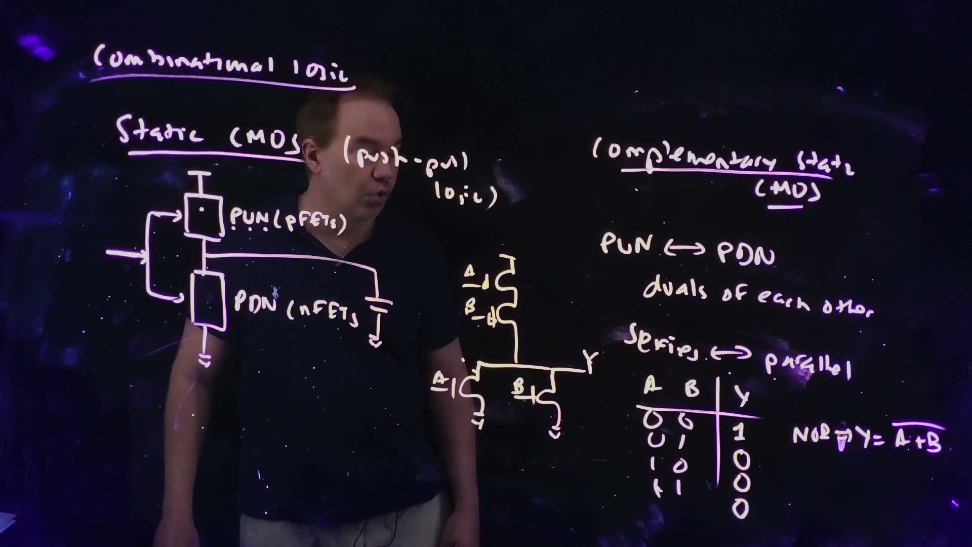
Why we need more than the inverter
So far the only gate is the inverter, and “obviously we can’t make a computer with an inverter”: it is not logically complete (25:54). We need general combinational gates; sequential elements (latches, flip-flops) come later (26:22).
What “static” means
The structure (27:13) board:
- a pull-up network (PUN) of PFETs between and the output;
- a pull-down network (PDN) of NFETs between the output and ground;
- the load capacitance on the output.
The gate is static CMOS if, for every static set of inputs, exactly one network is on (27:44–28:15): either the pull-up connects the output to or the pull-down connects it to ground. Never both, never neither. The other cases are other logic families, both taken up later (28:15):
- both on: ratioed logic;
- both off: dynamic logic.
Static CMOS is also called push-pull logic board: one network pushes the output up, the other pulls it down (28:44).
Complementary static CMOS: duals
The simplest way to guarantee the static condition is complementary static CMOS (28:56) board: the two networks are duals of each other. In terms of switches, wherever one network has a series connection, the other has a parallel one (29:41–30:01) board. Complementary always means static; static does not always mean complementary (29:16; Section 6 shows one).
The NOR (board, 30:01–31:56)
- Pull-down: two NFETs, A and B, in parallel. The dual pull-up: two PFETs in series.
- A = 0, B = 0: both NFETs off, so the pull-down is off; both PFETs on, so the pull-up is on. Y = 1.
- A = 0, B = 1 (or A = 1, B = 0): one NFET is on, so the pull-down is on; one PFET is off, so the series pull-up is off. Y = 0.
- A = 1, B = 1: Y = 0.
- Y is 1 only when neither input is 1 board: , a NOR.
Swap the roles (32:08): NFETs in series, PFETs in parallel. The pull-down conducts only when both inputs are 1, so , a NAND board. The lecturer leaves the truth table to you (32:39); the widget has it.
What to notice.
- For every input combination of NOR, NAND and AOI, exactly one network is green: the readout never says “contention” or “floating”. That is what “static” means.
- Series devices conduct only if all are on; parallel devices if any one is. The pull-up of a NOR is a series stack, so it conducts only for A = B = 0.
Check yourself Write the truth table of the two-input NAND and say which network is on in each row.
A = 0, B = 0: both parallel PFETs on, series NFETs off, Y = 1. A = 0, B = 1 and A = 1, B = 0: one PFET on (enough, they are in parallel), the series NFETs off, Y = 1. A = 1, B = 1: both PFETs off, both NFETs on, Y = 0. Exactly one network conducts in every row, so the gate is static.
Check yourself A gate's pull-up and pull-down are both on for one input combination. Is it static CMOS? What happens to the output?
No. Static CMOS needs exactly one network on. With both on, the output is a contest between the two networks, the situation the lecture calls ratioed logic (28:15); the output settles somewhere between the rails, set by their relative strengths.
5. Pin swapping, AOI gates and the stack limit
The idea. Gates with series stacks can be built in more complex forms, but each stacked device makes the gate slower. The device nearest the output is the fastest, and stacks taller than about three are avoided.

Pin swapping
In a series stack, the order of the devices doesn’t change the logic (33:18–34:15). A NAND is still a NAND with A and B exchanged in its NFET stack; a NOR is still a NOR with its PFETs exchanged. Exchanging them is called pin swapping board.
The delay does change (34:15): for a single input switching, the transistor closer to the output switches with less delay than the one further away. So a late-arriving signal should go to the input nearest the output (34:45–35:23). The lecture states the rule and promises the reason later; Chapter 8 (Lecture 8) gives it.
AND-OR-invert
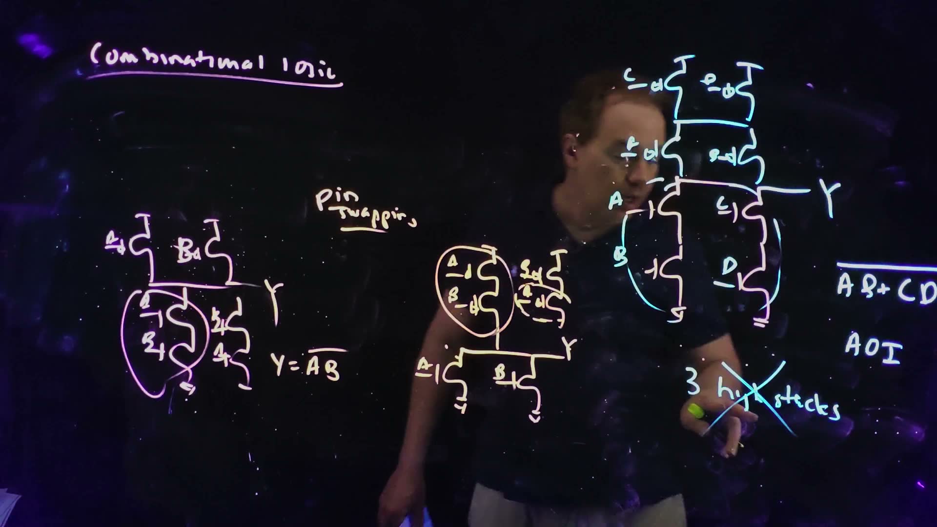
A more complex pull-down (35:49–37:25) board: A and B in series, in parallel with C and D in series. The dual pull-up has A and B in parallel, in series with C and D in parallel. The pull-down conducts when is true, so
an AND-OR-invert (AOI) gate board. Pin swapping applies here too: the AB and CD branches could change places (36:52). Choose AOI in the widget above to try it.
What limits a gate’s complexity
Why not put a whole block of logic into one huge gate (37:25)? Stacks. In a tall stack, the devices far from the output switch very slowly (37:53) board:
- two high: no problem;
- three high: questionable, but sometimes acceptable;
- more than three high: practically never (38:20).
That is what limits how much logic goes into a single stage of static CMOS.
Check yourself A four-input NAND (all NFETs in one series stack) has one input that arrives much later than the other three. Which stack position should it get, and why?
The position nearest the output. A single input switching near the output gives a shorter delay than one switching at the bottom of the stack (34:15), so the late signal should use the fastest input. (MT17-3d asks how the bottom input compares: it is slower. The reason is in Chapter 8.)
6. A static gate that is not complementary
The idea. If the inputs are guaranteed to come with their complements, some of a dual network’s connections become unnecessary. The gate is still static, though no longer a strict dual.
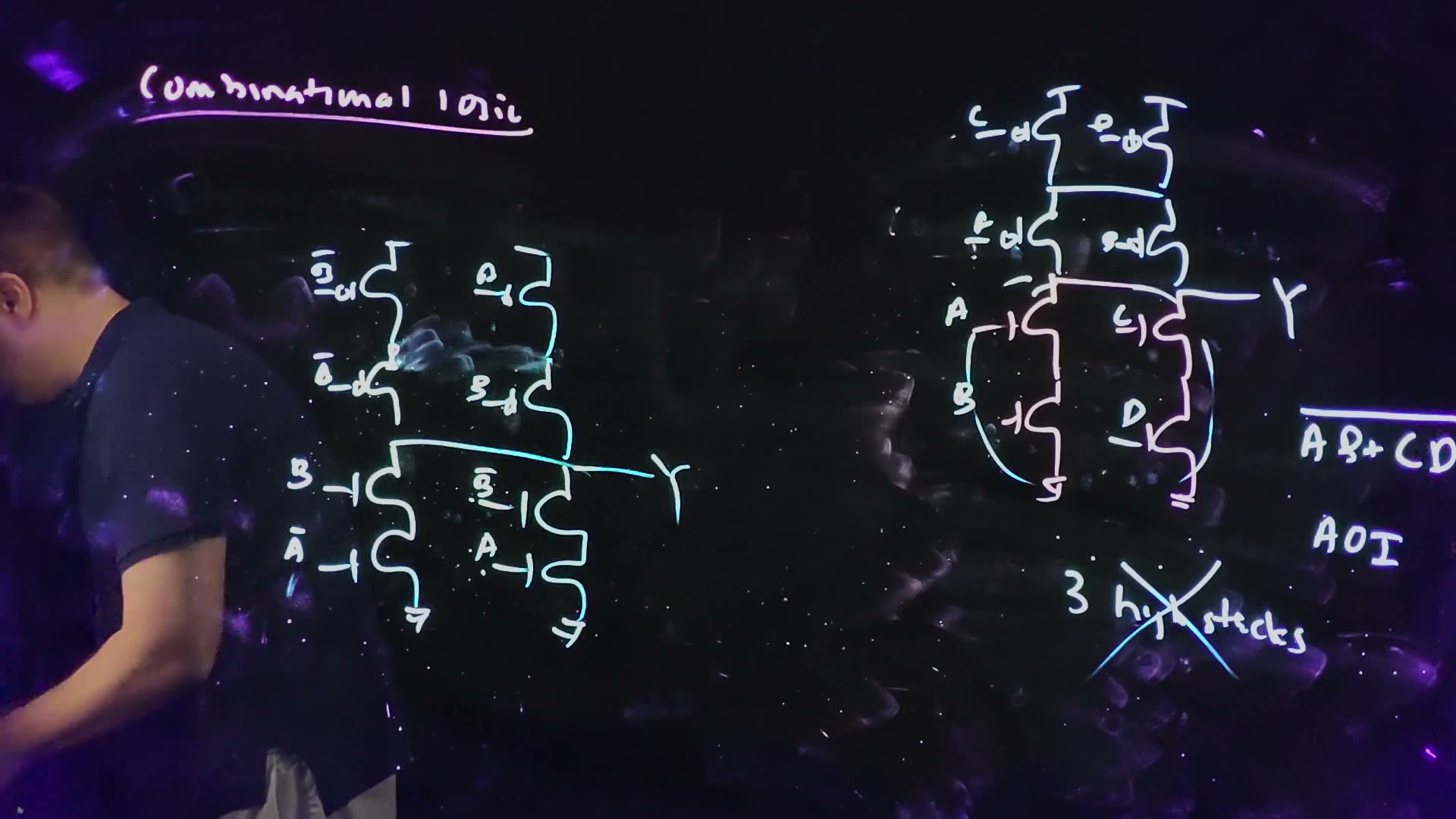
The lecture’s example (38:52–41:15) board:
- the inputs come in complementary pairs: A with Ā, B with B̄, and whatever drives them guarantees that each pair is always opposite (39:31);
- the pull-down: B in series with Ā, in parallel with B̄ in series with A;
- its dual pull-up: B̄ and A in parallel, in series with Ā and B in parallel. Drawn as two columns, B̄ over Ā and A over B, with a link between the middles of the columns (40:08).
The claim (40:20): removing the link changes neither the logic function nor the static behaviour, because the input constraints hold. The result is a static CMOS gate whose networks are not duals (40:44). The lecturer leaves the proof as an exercise.
The proof (added)
- Pull-down: it conducts when , that is, when A and B differ.
- Pull-up with the link: the PFET pairs conduct when and are both true. Multiplying out with : , that is, when A and B are equal.
- Pull-up without the link: the left column (B̄ over Ā) conducts when and ; the right column (A over B) when and . Together: , the same.
- In every one of the four allowed input combinations, exactly one network conducts. The gate is static, and : an XNOR (the lecture doesn’t name it).
Choose the two “constrained gate” settings in the widget of Section 4 and compare the truth tables. Then press “Set all four inputs freely” added: with A = 0, Ā = 0, B = 1, B̄ = 1 the gate without the link has neither network on and its output floats, while the full dual still drives it. The link is only unnecessary because of the constraint.
Check yourself In the constrained gate without the link, take A = 1, B = 0 (so Ā = 0, B̄ = 1). Which devices conduct, and what is Y?
Pull-down: the B̄–A branch has both NFETs on (B̄ = 1, A = 1), so it conducts. Pull-up: the left column needs B̄ = 0 (it is 1), the right column needs A = 0 (it is 1); neither conducts. Only the pull-down is on: Y = 0, as an XNOR gives for unequal inputs.
7. The fan-out-of-one delay
The idea. With the delay model, the FO1 delay of an inverter is just , independent of its size. It becomes the unit in which all gate delays are measured: .
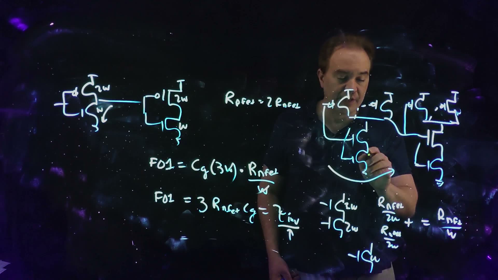
Back to our friend the fan-out of one (41:46): an inverter with a NFET and a PFET drives one identical inverter, with so that rise and fall are equal (42:02).
FO1 from the model (board, 42:19–43:26)
- The load is the next inverter’s input, of gate board: .
- Use the pull-down (the pull-up gives the same): resistance .
- Multiply board: .
- The widths cancel board: .
“Once I know my technology parameters, the and , I also can calculate my fan-out of one delay. Isn’t that nice?” (43:11). This delay is called , the basic unit of delay (43:26) board.
Compared with Chapter 5. added Lecture 5 found and showed that FO4 is less than four times FO1, because the driver’s own drain capacitance is paid only once. This model has no drain capacitance, so here . That is why bench 2’s delay in Section 3 equals .
Worked example. added With the numbers of Section 3, and : , and , the delay bench 2 measured. With the lecture’s 2 fF/µm and : .
Any load in units of τ_inv. added An inverter with NFET (PFET ) driving has delay : the load divided by the inverter’s own input capacitance, in units of . An extra fixed load (a wire, a side branch) just adds to .
Common mistakes.
- Counting only the NFET of the receiving inverter. Its input is the gate of both devices, .
- Expecting a bigger inverter to have a smaller FO1. It drives a bigger copy; the widths cancel. Size helps only against a fixed load.
- Assuming every exam uses . Some problems state that the NFET and PFET have equal strength; then the balanced inverter is and . added
Check yourself Cg = 1 fF/µm, Rnfet = 1 kΩ·µm, Rpfet = 2 kΩ·µm. A 2W/W inverter with W = 2 µm drives an identical inverter plus a 4 fF side load. What are τinv and the delay?
. The load is , the resistance , so the delay is . In units of : , and . (MT23-1d uses this stage delay.)
Check yourself A chain of four identical 2W/W inverters, each output also carrying a wire of Cx. τinv = 20 ps, Cg = 2 fF/µm. What is the delay through the chain for Cx = 0, and for Cx = 6 fF with W = 2 µm and with W = 10 µm? Which W minimizes the delay?
: every stage is an FO1, so , whatever . With the wire, each stage is . : , a stage is , the chain . : , a stage is , the chain . The delay keeps falling as grows: the wire becomes negligible next to the gates. (MT17-4a–b, MT21-4a, FN10-4a, MT24-2e.)
Check yourself With Rpfet = 2Rnfet and Cg = 2 fF/µm, an inverter with a 2 µm PFET and a 1 µm NFET drives 50 fF. Find both delays in units of τinv. Repeat with an 8 µm PFET.
50 fF is 25 µm of gate. Falling: . Rising with 2 µm: , also . Rising with 8 µm: ; the falling delay is unchanged. (MT17-3a–b is this problem with equal-strength devices, where .)
Check yourself An inverter sized Wp/Wn = n µm/1 µm drives an identical inverter (Rpfet = 2Rnfet). Write its falling and rising delays in units of RnfetCg. Which gives the smaller sum of the two, n = 2 or n = 1.5?
The load is µm of gate. Falling: . Rising: . For : . For : , smaller: a narrower PFET loads the previous stage less, and that wins more on the falling edge than it loses on the rising one. (MT21-4c finds the best , , by calculus; the exam kit does it.)
Check yourself From HW3 you have Cg = 1 fF/µm, Rnfet = 3 kΩ·µm and Rpfet = 6 kΩ·µm. An inverter with an 8 µm PFET and a 4 µm NFET drives an identical inverter. Estimate tpLH and tpHL.
The load is . and . (HW4-1b does this with its own characterized values.)
8. Sizing stacks and logical effort
The idea. To give a NAND or NOR the same drive as an inverter, the stacked devices must be made wider. Wider devices mean more input capacitance for the same drive, so the gate is slower than an inverter by a fixed factor: its logical effort.
Two devices in series
Treat stacked transistors like resistors in series (45:29) board:
The stack rule (board, 45:29–46:28)
- Two NFETs in series, each of width . Each has resistance .
- In series the resistances add board: .
- That is the resistance of a single NFET of width board.
- So a stack of two needs each device twice as wide to keep the strength of one device. (“Zero order”, the lecturer adds (46:00).)
added The same counting for a stack of three: each device , since .
NAND driving NAND
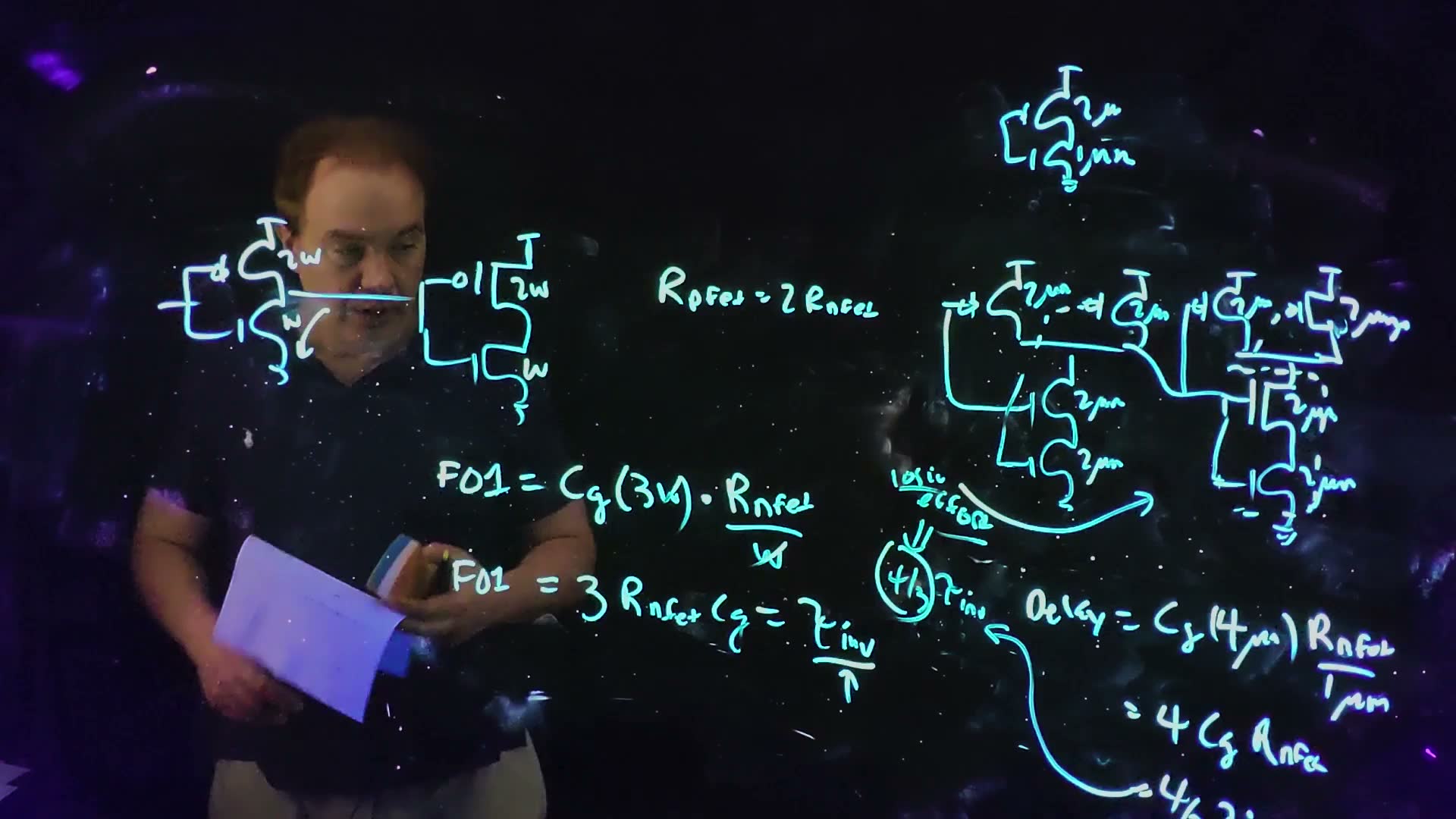
Size a NAND to match a 2/1 µm inverter (46:28–47:12) board:
- its two NFETs are in series, so each is 2 µm: together they act like the inverter’s 1 µm NFET;
- its two PFETs are in parallel, each 2 µm, like the inverter’s 2 µm PFET. added Why not 1 µm each, since two in parallel make 2 µm? Because when only one input falls, only one PFET turns on, and it alone must match the inverter’s pull-up. Sizing is for the worst case.
Now let the NAND drive an identical NAND (47:25):
NAND logical effort (board, 47:47–50:31)
- One input of the receiving NAND is the gate of one 2 µm NFET and one 2 µm PFET: of gate board.
- The driving NAND pulls down with the strength of a 1 µm NFET, .
- Delay board: .
- Since board: delay .
Why 4/3 (49:16). The NAND has the same drive strength as the 2/1 inverter, but it presents 4 µm of input capacitance instead of 3 µm. Building the more complex function needed a stack, the stack needed larger devices, and larger devices are more capacitance to drive. (At 49:03 the lecturer says “four thirds the drive strength”; he means four thirds the delay, as he said a sentence earlier and as the board writes.)
This number, , is the logical effort of the NAND (49:47) board. It is a property of the gate’s structure: with every device instead of 2 µm, the same calculation gives again (50:03).
NOR driving NOR
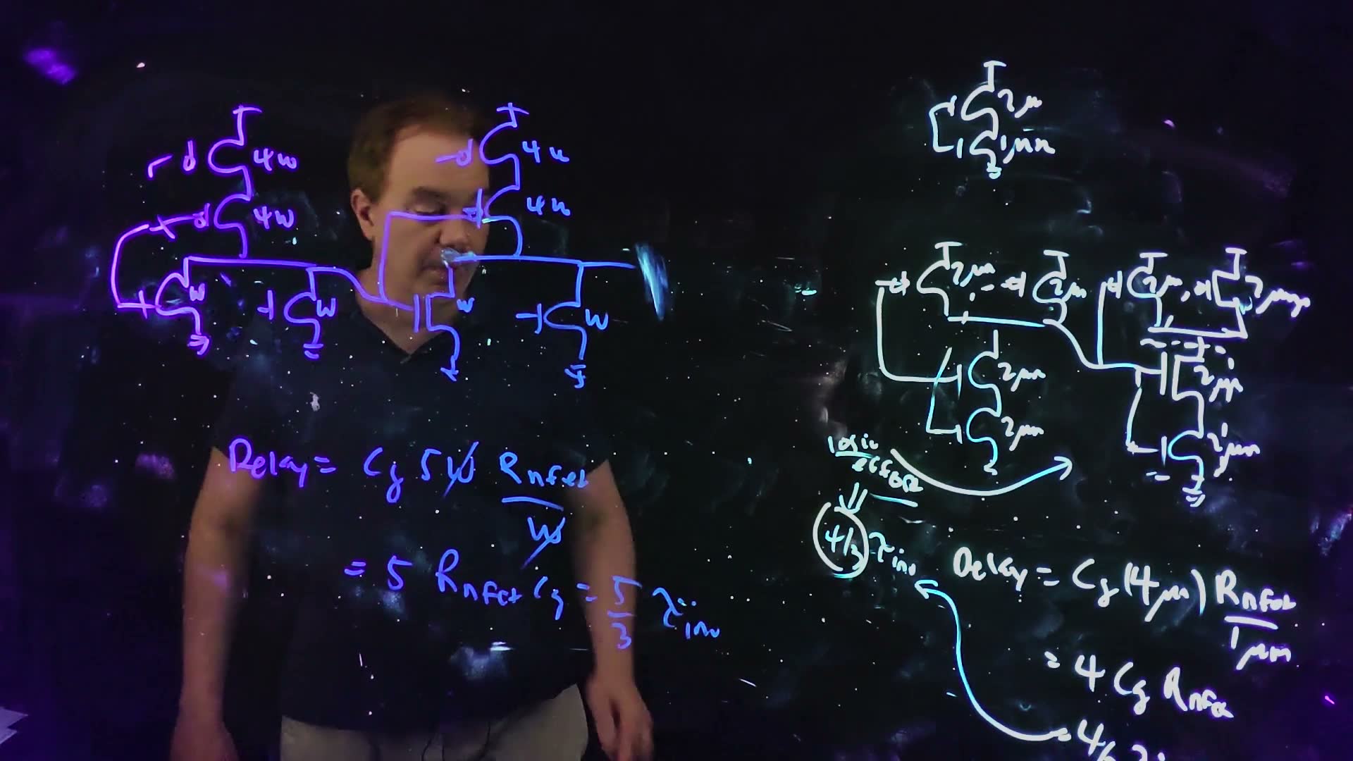
Will the NOR’s logical effort be better or worse (50:35)? Worse: the NOR stacks the PFETs, which are already twice as large, and stacking doubles them again (51:06).
NOR logical effort (board, 52:43–53:52)
- NFETs in parallel, each : one alone has the strength of the inverter’s NFET.
- A single PFET would need ; two in series need twice that: each board.
- One input: of gate.
- Delay board: .
The logical effort is 5/3, worse than the NAND’s 4/3, “just as we suspected” (53:52).
Compare the gates, and see what the fan-out and an extra load do:
What to notice.
- With fan-out 1 the delays are , and , whatever , or : logical effort is a pure number.
- Each line’s slope is its logical effort. NOR2 and NAND3 lie on top of each other: both have .
- Add an extra load and the delay depends on again; a larger helps (Section 7’s chain).
Worked example. added With (Section 3’s technology): a NAND driving a NAND takes , a NOR driving a NOR . The NAND is the faster of the two.
Common mistakes.
- Counting all four transistors of the receiving gate. One input connects to one NFET and one PFET; only those are its load.
- Sizing the parallel devices as if they all turn on together. A single one may be the only one on.
- Forgetting that the PFET doubling and the stack doubling multiply in the NOR: .
Check yourself Size the AOI gate of Section 5 for the drive of a 2W/W inverter, and find its logical effort for input A.
Pull-down: each branch is a stack of two NFETs, so each is . Pull-up: two parallel pairs in series, a stack of two PFETs in the worst case, so each PFET is . Input A drives one NFET and one PFET: of gate. .
Check yourself A four-input NAND has all four NFETs and all four PFETs 4 µm wide; it drives 50 fF, with Cg = 2 fF/µm and Rpfet = 2Rnfet. Find the falling and rising delays in units of τinv.
50 fF is 25 µm of gate. Falling: four 4 µm NFETs in series act as one 1 µm NFET, so . Rising: one 4 µm PFET, . (MT17-3d, with equal-strength devices in the original.)
9. Electrical effort and gain
The idea. A gate’s delay is the product of two factors: its logical effort (how much harder its structure is to drive than an inverter’s) and its electrical effort (how much load it drives compared with its own input). The product is the gate’s gain, and the delay is gain × .

Let the NAND drive two NANDs of its own size (54:35):
Gain (board, 54:57–56:20)
- The load doubles: two inputs of 4 µm each board: .
- Delay board: .
- The is the logical effort, board.
- The extra factor 2, from fanning out to two gates of the same size, is the electrical effort, board. In the Sutherland and Sproull book they are called and (55:53).
- Their product is the gain of the gate board: .
The gain is “the factor that I multiply by , the unit inverter delay, to get the delay of that gate given its loading” (56:20).
What comes next (56:31). The next lecture uses gains to estimate the delay of any path through logic “very quickly and easily”, and then to choose the transistor widths along a critical path that minimize its delay: gain-based tuning, also called the method of logical effort, after the Sutherland and Sproull book on the course reserves (57:04). added Since each gate’s delay is its own gain times , a path’s delay is the sum of the gains along it, times .
Worked example. added With : the NAND driving two NANDs takes . Set the widget of Section 8 to NAND2 with fan-out 2 to see it.
Check yourself An inverter (2 µm PFET, 1 µm NFET) drives one input of a NAND sized like the lecture's (every device 2 µm). The NAND drives 60 fF. With Cg = 2 fF/µm and Rpfet = 2Rnfet, what is each stage's gain, and the total delay in τinv?
Inverter: , , gain . NAND: ; 60 fF is 30 µm of gate, so and the gain is . Total: . Check the NAND directly: . (MT17-5a and MT23-5a add gains this way along four stages.)
Check yourself A NOR (logical effort 5/3) drives three NORs of its own size. What is its gain? With τinv = 15 ps, what is its delay?
, so the gain is , and the delay .
Formulas to remember
| Formula | Meaning |
|---|---|
| ; | the simplified delay model; is a fitted constant (no ln 2) |
| gate capacitance per micron; constant under scaling | |
| , in kΩ·µm, | resistance times width; divide by |
| bench 1: match to an 8(16/8) input | |
| , | bench 2, ; AS = AD = PS = PD = 0 |
| exactly one of PUN, PDN on | static CMOS (both on: ratioed; both off: dynamic) |
| PUN and PDN duals: series ↔ parallel | complementary static CMOS |
| , , | NOR, NAND, AOI |
| late signal on the device nearest the output; stacks ≤ 2, maybe 3 | pin swapping; the stack limit |
| the unit of delay; FO4 = in this model | |
| stack of : each device wider | equal drive |
| , | logical effort, |
| delay , | gain |
The lecture’s boards