M6. Past midterms: dynamic and domino logic
This page works every past-midterm problem on dynamic and domino logic. The family has grown on each recent exam: 8 of 150 points in 2017 (a single delay), 32 of 150 in 2023 (a whole question), 50 of 200 in 2024 (a whole question, the largest on the paper). Both recent questions use a p-type dynamic stage, the polarity that Lecture 12 introduces for NP domino, so read Chapter 12, Section 6 first if it is new to you.
Every answer below is re-solved here; none is copied from an answer key. Where a key disagrees, the folded note on the key at the end of the part explains why, and the table at the end lists them all. Two problems from past finals follow the midterm questions as extra drills, because the midterms have only one domino-sizing problem and none on clocking two dynamic stages.
After this page you can:
- read the function of a dynamic stage, n-type or p-type, and follow a cascade of them to its outputs;
- find the one edge each stage makes along a path, and notice when a question names an edge the circuit cannot make;
- compute an evaluate delay by and by dynamic logical effort, with the whole stack counted from the rail to the node, in either strength convention;
- resize a path whose widths also sit beside fixed loads or fixed devices, where equal gains are no longer exact;
- explain what skewing the inverter after a dynamic node does to its noise margins, and add the half latch that protects the node;
- time two dynamic stages on two clocks: the race, and the collision a footless stage risks.
Before you start
How to use this page. Each section restates one exam question with its source page (MT23-3b, p8 is Fall 2023, question 3b, physical PDF page 8) and its points, and shows the exam’s own figure. The page opens with a short How to approach section: how to recognize a dynamic-logic question, the moves in order, why the formulas apply, and the traps. Then every part is worked the same way: what it asks, the idea behind the method, the solution in steps (each step gives its reason first), a check on the result, the answer, and one thing to remember. Try each part on your own first; open the Hint if you are stuck, and step through the solution before you press “Show all”. The answer key’s verdict is folded at the end of each part. The chapters teach each method in full, and every solution links the section.
| Question | Parts | Points | Chapters |
|---|---|---|---|
| MT24-5 | function, delay, resizing | 50 (of 200) | 8, 11, 12 |
| MT23-3 | function, delay, noise margins, half latch | 32 (of 150) | 6, 7, 11, 12 |
| MT17-3c | evaluate delay | 8 (of 150) | 7, 11, 12 |
| FN12-8 (final) | delay, sizing | 30 (of 200) | 8, 12 |
| FN17-2 (final) | race, collision, function | 25 (of 250) | 11, 12 |
MT21 has no dynamic question. The other parts of MT17-3 (static inverters and a NAND4) are on page M3.
Conventions the exams use
- n-type and p-type stages (Chapter 11, Section 4; Chapter 12, Sections 5–6). An n-type stage is precharged to 1 by a clocked PFET and evaluates through NFETs; its node is , where is the network’s conduction function, and the domino inverter after it gives . A p-type stage is pre-discharged to 0 by a clocked NFET and evaluates through PFETs, which conduct on 0s; its node is . Which clock phase evaluates depends on how the clocked devices are wired: read it from the figure.
- The logical edge (Chapter 12, Section 1). In evaluate an n node can only fall and a p node can only rise. So along a path each stage makes exactly one edge, and the inverter after an n node rises, the one after a p node falls. Find the edges before you choose a resistor.
- Strength conventions. “The nFET and pFET have the same strength” (MT17-3, MT24-5): the balanced inverter is W/W, , and a -high stack of equal devices has , n-type or p-type. With (MT23-3, FN12-8, FN17-2): , for an n stage and for a p stage (Chapter 12, Section 2).
- Stacks. Count every device between the rail and the node, the footer (n) or the clocked header (p) included; the precharge or pre-discharge device is off during evaluate and never counts. Equal devices in series: (Chapter 7, Section 8).
- Delay , or ; the two agree. MT23-3b’s key multiplies by 0.69; where it matters this page gives both. Loads are written as widths: µm of gate.
- Names. Node names added on this page: X and Z in MT24-5 (the outputs of its stages 1 and 2). The exams’ own names (W1–W9, M1–M9, Vn, Y1, Y2, I–IV) are kept.
How to approach a dynamic-logic question
Recognize it by the clock. Some transistors have clk (or , or ) on their gates: a clocked PFET from to a node, a clocked NFET from the node or the network to ground, and a network of logic transistors between them. Often an inverter follows the node. The exams ask “what logic function does this circuit perform”, “the delay from A falling to Y falling”, “resize … to minimize the delay”, “how do the noise margins compare”, “add a transistor”, or, on the finals, how two clocks must be timed. The family carried 8 of 150 points in MT17, 32 of 150 in MT23 and 50 of 200 in MT24, the largest question on that paper.
The moves, in order.
- n-type or p-type, and which phase evaluates. Read the clocked devices. A clocked PFET above an NFET network precharges the node to 1: an n-type stage, which evaluates while that PFET is off. A clocked NFET below a PFET network pre-discharges the node to 0: a p-type stage, which evaluates while that NFET is off. Whether that is clk = 1 or clk = 0 depends on which clock drives the device, so read it from the figure.
- The node’s function. Write the network’s conduction function : series devices are AND, parallel ones OR, and a PFET conducts on a 0. An n node is ; a p node is . Then follow the inverters.
- The one edge each stage can make. In evaluate an n node can only fall and a p node can only rise; the inverter after an n node rises, the one after a p node falls. Mark the edges along the path before you pick any device, and check that the edge the question names is one the path can make.
- The delay, with the whole stack. Count every device in series from the rail to the node: the footer (n) or the clocked header (p) is in, the precharge device is out. Then use or .
- Resizing. For each width you may change, ask what it drives and what it loads. If it also loads a fixed branch, or sits beside a fixed device, the path effort moves with it and equal gains are no longer exact: balance the parts that change.
- Noise. The inverter after a dynamic node is skewed toward the edge that carries the logic. That moves its threshold toward the node’s resting value and shrinks the margin that protects the node. A half latch holds the resting value.
- Two clocks. A second dynamic stage must not start evaluating before the first has finished (a race), and a footless stage must not precharge while its input is 1 (a collision).
Why these formulas.
- The function. In evaluate the precharge device is off, so the node changes only if the network conducts. An n node is pulled to 0 exactly when its NFETs conduct, so it is ; a p node is pulled to 1 exactly when its PFETs conduct, so it is (Chapter 11, Section 4; Chapter 12, Section 6).
- The delay. The course models a conducting transistor of width as a resistor , with in kΩ·µm; 1 kΩ × 1 fF = 1 ps. Devices in series carry the same current, so their resistances add, and of them act like one device of width (Chapter 7, Section 8). The evaluate delay is then (Chapter 11, Section 4). The model fits best when the device nearest the node switches last, with the nodes below it already at the rail (Chapter 8, Section 10).
- Dynamic logical effort. Compare the stage with the balanced inverter that pulls as hard as its evaluate path added: for an n stage, and the mirror, , for a p stage. For a -high stack of equal devices that is at equal strengths, and (n) or (p) with . An input drives only its own devices, never a PFET partner, which is why a dynamic stage beats a static gate (Chapter 12, Sections 2 and 6). The path delay is , with the load over the input (Chapter 8, Section 2).
Decisions to make on the way. The strength convention: it sets ( at equal strengths, with ) and every . Which edge the path makes. Which node a load hangs on, and which gates sit on each node. Whether to multiply by 0.69: the chapters don’t; say so when a key does.
Traps. An edge the circuit cannot make (MT24-5b, FN17-2c). Dropping series devices because an internal node is “precharged” (MT23-3b). Leaving out the footer or header, or counting the precharge device. The wrong strength convention (MT17-3c: 9.375 or 6.25 ). for on a p node (MT23-3c). Holding fixed while the widths you change move a branch (MT24-5c). Delayed reset when no inverter follows the first stage (FN17-2b).
1. MT24-5: a dynamic full adder
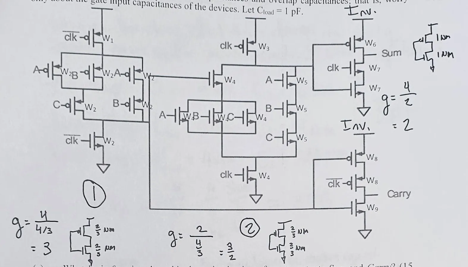
MT24-5, p10–12 (Fall 2024, 50 points). Consider the dynamic logic circuit shown above. In this technology, the nFET and pFET have the same drive strength. The gate capacitance per unit width is 1 fF/µm. Assume that the FO1 delay is ps. A minimum width device is 1.0 µm. Please ignore source-drain diffusion capacitances and overlap capacitances; that is, worry only about the gate input capacitances of the devices. (a) What logic function does this dynamic circuit perform to outputs Sum and Carry? (15 points) (b) Estimate the delay of the critical path from A falling to Sum falling. In this case, assume Sum is loaded with 500 fF of capacitance and let . (15 points) (c) Now resize and with the goal of minimizing the delay of this path. What is the new path delay? (20 points)
(The stem also says pF; part (b) replaces it with 500 fF on Sum.) Read the circuit once, stage by stage, before answering anything.
Reading MT24-5 stage by stage
- Clocks first, because they decide what kind of stage each one is. W1 (a PFET) and the bottom NFET W2 of stage 1 are on ; W3 (a PFET) and the bottom W4 of stage 2 are on clk; one W7 of the Sum stage is on clk, one W8 of the Carry stage on .
- Precharge, clk = 0, to find each node’s resting value. , so W2 is on and pre-discharges stage 1’s node, which we call X, to 0; W3 is on and precharges stage 2’s node, Z, to 1. The clocked W7 (gate clk = 0) and W8 (gate ) are off, so Sum and Carry are cut off from one rail and hold their values.
- Evaluate, clk = 1, to find the type of each stage. W1 turns on and W2 off: X is no longer held at 0 and can only be pulled up through PFETs, so stage 1 is a p-type stage, and X rises if its PFETs conduct. W3 turns off and the footer W4 on: Z can only be pulled down through NFETs, so stage 2 is an ordinary n-type stage, and Z falls if its NFETs conduct. This is Lecture 12’s NP arrangement (Chapter 12, Section 5), with the header PFET and the pre-discharge NFET both on , as they must be: the p stage evaluates in the same phase as the n stage.
- Networks, because they give the functions and the stacks. Stage 1, from W1 down to X: (A ∥ B) in series with C, all in parallel with A in series with B. Stage 2, from Z down to the footer: the NFET gated by X in series with (A ∥ B ∥ C), all in parallel with A, B, C in series (the W5 devices).
- Output stages, because they set the last edge and the loads on X and Z. Sum: the PFET W6 (gate Z) pulls Sum up; the two W7 NFETs (gates clk and Z) pull it down. Carry: the two W8 PFETs (gates X and ) pull up; W9 (gate X) pulls down. In evaluate the clocked devices are on, so these are inverters, Sum and Carry ; in precharge they hold. So X carries three gates (the X-input NFET, one W8 and W9) and Z two (W6 and the lower W7).
MT24-5a: the functions
MT24-5a, p10 (15 points). What logic function does this dynamic circuit perform to outputs Sum and Carry?
Hint
What it asks. The Boolean functions that appear at Sum and Carry once the circuit has evaluated, as functions of A, B and C. “Dynamic circuit” tells you to read each node in the evaluate phase, stage by stage, with the polarity you found above.
The idea. In evaluate the precharge device is off, so a node changes only if its network conducts. Write each network’s conduction function: series devices are AND, parallel ones OR, and a PFET conducts when its gate is 0, so a PFET gated by A contributes . An n node is pulled to 0 when its NFETs conduct, so it is the complement of its network’s function; a p node is pulled to 1 when its PFETs conduct, so it equals its network’s function (Chapter 11, Section 4; Chapter 12, Section 6). The tempting slip is to treat stage 1 like an n stage and complement it: that swaps Carry and its complement.
Sum and Carry
- Stage 1’s network, with each PFET’s input complemented. A PFET conducts when its gate is 0, so A contributes , and so on. Series is AND and parallel is OR, so the network conducts when .
- Simplify, to recognize it. By De Morgan, and , so the sum is .
- X and Carry. A p node equals its network’s conduction function: , the complement of the majority. The Carry stage inverts X: Carry .
- Stage 2 and Sum. Its NFETs conduct on 1s: the X-input NFET in series with the parallel A, B, C gives , and the three series W5 devices give , so the network conducts when . An n node is the complement of that, and the Sum stage inverts it again: Sum .
- Read Sum by the number of inputs at 1, because X depends only on that count. None: and , Sum = 0. One: X = 1 (no majority) and , Sum = 1. Two: X = 0 and , Sum = 0. Three: , Sum = 1. Sum is 1 for an odd count: .
Check. A full adder must satisfy Sum + 2·Carry = A + B + C, the number of inputs at 1, in binary. Zero ones: 0 + 0 = 0. One: 1 + 0 = 1. Two: 0 + 2 = 2. Three: 1 + 2 = 3. ✓ All eight rows pass.
Answer: Sum and Carry : a full adder. Stage 1 computes and stage 2 reuses it, which is why its network is so small.
Remember. An n node is NOT f, a p node is f; then count the inverters. When a later stage takes an earlier node as an input (X here), it is reusing a result: say what that result means.
The answer key agrees
MT24-5b: the delay
MT24-5b, p11 (15 points). Estimate the delay of the critical path from A falling to Sum falling. In this case, assume Sum is loaded with 500 fF of capacitance and let all of to be 2 µm.
Hint
What it asks. The delay along the path A → X → Z → Sum, with every width 2 µm and 500 fF on Sum, in units of ps and then in ns. The words “A falling to Sum falling” name the two edges, and the first job is to test them: each dynamic stage can make only one edge in evaluate, so the edges along the path are fixed by the circuit, not by the question.
The idea. Find the edge each stage makes, because the edge decides which devices carry the current, and so the logical effort. Then add the stage gains: delay (Chapter 8, Section 2). Each compares the stage with the balanced inverter that pulls as hard as the devices making that edge, with the whole stack from the rail counted (Chapter 12, Sections 2 and 6). Each is all the gate on the node over the stage’s input. With equal strengths the balanced inverter is W/W, a -high stack has , and . The tempting move is to take “Sum falling” as given and use the W7 pull-down. That is an edge the clock makes, not A.
Which edges, then the efforts
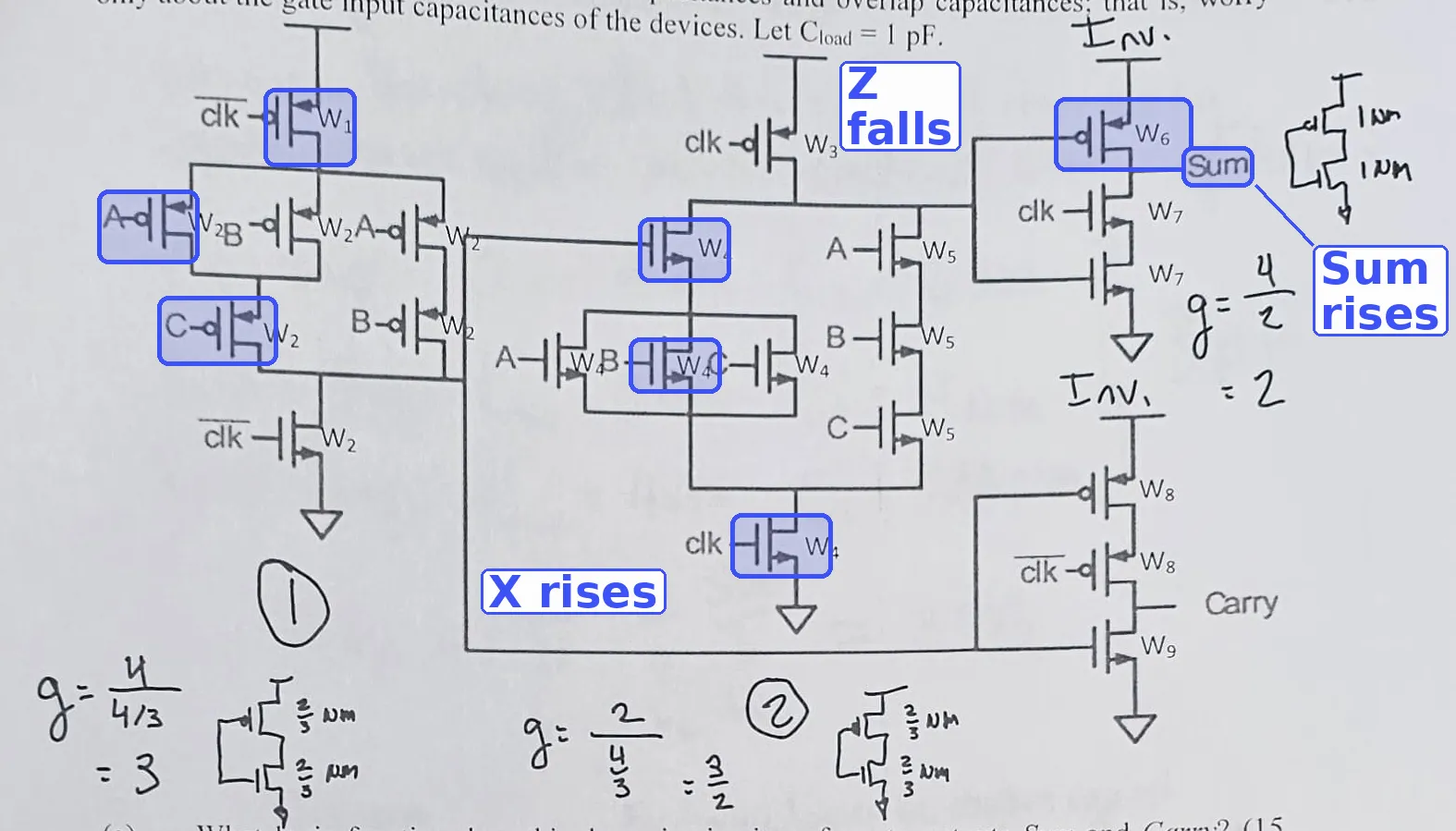
- Follow the edges from A. Inputs to a p stage evaluate by falling: A falling can turn on its PFETs, so X can only rise. X rising turns on stage 2’s X-input NFET, so Z can only fall. Z falling turns W6 on and the lower W7 off, so Sum rises. (A also drives stage 2’s A NFETs directly, but A falling only turns them off, and an n node cannot rise in evaluate.)
- Test it on one input pattern. B = 1, C = 0, and A falls from 1 to 0 during evaluate. Before: a majority, so X stays 0, Z stays 1 and Sum is pulled to 0 through the two W7s as soon as clk rises. After: no majority, X rises, Z falls through the X-input NFET and B, and Sum rises to .
- So the path ends with Sum rising. Sum can fall only through the W7 stack while Z stays high, and that happens when the clock rises, not because A fell.
- Stage 1’s effort, with the header counted. The current that lifts X flows from through W1, A and C (or W1, A and B): three 2 µm PFETs in series, . The W/W inverter with that pull-up has input . A appears twice in the network, so it drives two PFETs, 4 µm: .
- Stage 2’s effort, with the footer counted. Z discharges through the X-input NFET, one of A, B, C and the footer: again three 2 µm devices, , reference . X drives one 2 µm NFET: .
- The Sum stage on its rising edge. W6 alone pulls Sum up, so the reference is a 2/2 µm inverter (4 µm). Z drives W6 and the lower W7, : .
- Electrical efforts: every gate on each node. X drives the X-input NFET and the Carry stage’s W8 and W9 (the other W8 is on ): ; the Carry stage is a branch off the path. Z drives W6 and W7: . Sum: .
- Add the gains. Delay .
Check. The big term by : W6 is driving , that is with . ✓ Both routes agree, as they must: logical effort is the same model in other units.
Answer: about ns, almost all of it the 2 µm PFET W6 driving 500 fF. The edge this path makes at the output is Sum rising.
Remember. In a dynamic path the edges are set by the stages, not by the question’s wording: n nodes fall, p nodes rise, and each inverter flips the edge. If the named edge is impossible, say in one line which edge you compute and why.
The answer key differs
It uses (a reference inverter with 1 µm devices, the strength of the two W7s in series) and gets 12.875 ns (). That is Sum’s falling edge, which a falling A cannot cause. Its , and all three values are right. The rubric gives 13 of the 15 points to the values, the values and the delay formula. If you follow the question’s wording instead, the falling edge gives the key’s .
MT24-5c: resizing W4 and W7
MT24-5c, p12 (20 points). Now resize and with the goal of minimizing the delay of this path. What is the new path delay?
Hint
What it asks. Choose and (every other width stays 2 µm) to make the delay of (b)‘s path as small as possible, and give the new delay. Each name covers several devices: is all five devices labelled W4 in stage 2, both NFETs of the Sum stage. “Resize and ” therefore means two numbers, and the first job is to see where each one enters the delay.
The idea. Write the delay as a function of the two widths, and ask of each width what it drives and what it loads. A width that only adds load to the path belongs at the minimum. A width that drives one stage and loads the one before would normally be set by the equal-gain rule, (Chapter 8, Section 3). But that rule needs a fixed product of gains, and here X also drives the Carry stage, a fixed 4 µm that does not grow with : the branch, and with it , changes as changes (Chapter 8, Section 8). So balance only what changes. Making larger loads X more (stage 1 slows by , with the input of stage 1) and makes stage 2 stronger (its gain, , shrinks, with the load on Z). Their sum is least where the two are equal, which gives . The tempting route, the key’s, is to hold at its part-(b) value and take ; the widths it then picks change that very .
Resizing for the edge this path makes (Sum rising)
- List what each width touches, because a width can speed up only the stage it drives. drives Z: all of stage 2 scales with it, so stays and . It also loads X: . loads Z through the lower W7. But Sum’s rising edge is W6 alone, so the Sum stage’s gain is whatever is.
- Write the delay. .
- is pure load: take the minimum, 1 µm. It appears only on top of stage 2’s fraction. A wider W7 adds gate to Z and does nothing for W6, the only device that lifts Sum.
- Balance what changes. With , , and only moves with ; the 3 is the Carry branch’s fixed share of stage 1. One part grows with and one shrinks, so the sum is least where they are equal: , . That is (the Fall 2026 recitation’s form), with , , , . At the optimum, the delay adds to stage 1 by loading X equals stage 2’s whole gain. The stage gains, 4.84 and 1.84, are not equal, because stage 1 also carries the fixed branch.
- The delay. . Leaving at 2 µm, gives .
- Why the gain is tiny. of the path is W6 driving 500 fF, and W6 is not one of the widths you may change. Shrinking also slows Sum’s other edge, the clocked pull-down when the sum is 0 (); in a real design you would keep it.
The question’s choice of widths only makes sense for Sum’s falling edge, the one the key computes in (b): then drives Sum. Solved that way, with the sizes kept consistent:
If you read Sum's falling edge, as the key does
- The Sum stage now pulls down through the two W7s in series, so its gain is . stays 2 µm, so changes as grows: is not fixed.
- The branch at X moves too. It is , so (and with it ) is not fixed either. The delay is .
- Equal gains, kept consistent. Because moves, set all three gains equal to and solve for the widths that really give : , , and . That gives , , , delay .
- The exact minimum (the widget below) is at , : equal gains are within 2%.
Check. Try the neighbours on the rising edge: the part that moves, , is 3.75 at both and , and 3.67 at . The minimum lies between them, and it is shallow: the whole resizing saves only ().
Answer: on the edge the path of (b) makes (Sum rising), to the minimum, 1 µm, and : ns, barely better than (b), because the fixed W6 sets . On the falling edge the key intends: about ns, with – and –.
Remember. Before resizing, ask what each width drives and what it loads: pure load goes to the minimum. When a width also feeds a fixed branch, balance the delay it adds against the delay it saves; is only a guess.
The answer key differs
It says 2.25 ns with and . It takes from part (b), and , then sizes from and from . But its widths change its : with the first gain is , not 15, and with W6 held at 2 µm the Sum stage’s falling gain is , not 15. Its widths actually give on the falling edge (or even with its own ), not 2.25 ns. Its grading note admits that equal gains are “not exactly correct” with a branch. On the rising edge its widths make the path slower than (b): ns, because a 64.6 µm is pure load.
What to notice.
- On “Sum rises”, drag : the delay only grows. The dashed curve (with re-chosen) bottoms out at the left end.
- On “Sum falls”, press “the key’s sizes” and read : it is not 3375, and the stage gains are far from 15 each.
- In both readings changes as you move , because X also drives the fixed Carry stage. Compare FN12-8b (the second button), where nothing sits beside the resized widths: there stays fixed and the lowest delay has equal gains.
2. MT23-3: a p-type domino XOR
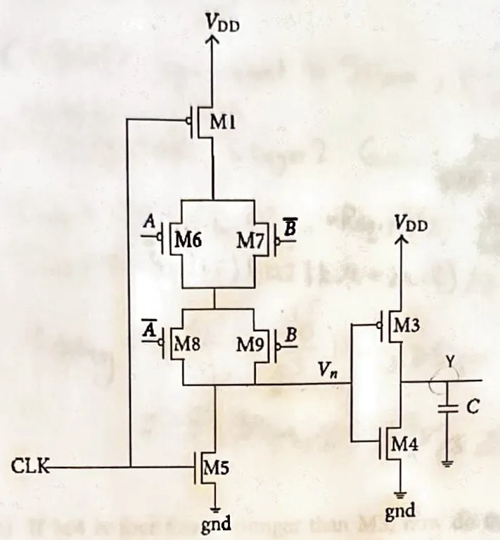
MT23-3, p7–9 (Fall 2023, 32 points). Consider the domino gate shown above. Let , and . Let C = 50 fF. (a) What logic function does this domino gate perform (Y as a function of A and B)? (8 points) (b) If M4 = 10 µm and M1 = M6 = M7 = M8 = M9 = 3 µm, what is the delay from B falling to Y falling? Assume that M4 is four times stronger than M3 (that is, at the same overdrive, it has four times the drain current). (10 points) (c) If M4 is four times stronger than M3, how do the static DC noise margins of this inverter compare with the case the M4 and M3 are sized for equal drive strength? How might this be significant in this circuit? (8 points) (d) How might the on be improved in this circuit with the addition of a transistor? (6 points)
Reading MT23-3
- The clocked devices first, because they decide the stage’s type. CLK drives M1, a PFET from , and M5, an NFET from to ground.
- The two phases. CLK = 1: M5 on, M1 off, so is pre-discharged to 0. CLK = 0: M1 on, M5 off, and the PFET network may pull up. The node rests at 0 and can only rise through PFETs, so this is a p-type stage, and it evaluates while CLK is low, the phase in which an n-type stage on the same clock would precharge (Chapter 12, Section 5).
- The network, because it gives the function and the stack. (M6, gate A ∥ M7, gate ) in series with (M8, gate ∥ M9, gate B).
- The inverter, because it sets the last edge and ‘s load. M3 (PFET) and M4 (NFET) invert to Y, which drives C. So carries the two gates M3 and M4.
MT23-3a: the function
MT23-3a, p7 (8 points). What logic function does this domino gate perform (Y as a function of A and B)?
Hint
What it asks. Y as a Boolean function of A and B, after the gate has evaluated. The words “domino gate” tell you there is a dynamic node and an inverter; the figure tells you that the node is p-type.
The idea. This is MT24-5a’s reading with a single p stage. A PFET conducts when its gate is 0, so write each PFET’s input complemented; parallel devices are OR, series ones AND. A p node is pulled up exactly when its network conducts, so it equals the conduction function, and the inverter complements it (Chapter 12, Section 6). The tempting slip is to read the PFETs as NFETs: that gives the complement of every term, and the opposite answer.
Y
- The upper pair. M6 conducts for A = 0 and M7 for B = 1, and they are in parallel: the pair conducts for .
- The lower pair. M8 conducts for A = 1 and M9 for B = 0: .
- The two pairs in series must both conduct: , the XNOR.
- The node and the inverter. A p node equals its network’s conduction function, so in evaluate , and .
Check. Walk the truth table through the transistors (A B → Y). 00: M6 and M9 on, a path from M1 to , so rises and Y = 0. 01: M6 and M7 on, but M8 and M9 off, so stays 0 and Y = 1. 10: M8 and M9 on, but M6 and M7 off, Y = 1. 11: M7 and M8 on, rises, Y = 0. ✓ That is the XOR.
Answer: .
Remember. For a p stage, complement each PFET’s input, then read series as AND and parallel as OR; the node is that function itself.
The answer key agrees
MT23-3b: the delay
MT23-3b, p8 (10 points). If M4 = 10 µm and M1 = M6 = M7 = M8 = M9 = 3 µm, what is the delay from B falling to Y falling? Assume that M4 is four times stronger than M3.
Hint
What it asks. The delay from B falling to Y falling, in ps, with the widths given and M3 not given: you know only that M4 is four times stronger. Two phrases decide the method: “B falling” picks the PFET that switches, and so the path; “four times stronger” sets M3’s width, which you need for ‘s load.
The idea. Each stage takes : the conducting devices act as a resistor that charges or discharges the node (Chapter 11, Section 4). Devices in series carry the same current, so their resistances add (Chapter 7, Section 8): three 3 µm PFETs at give . The clocked header M1 is one of them: it is on during evaluate and every bit of charge passes through it. The chapters don’t multiply by 0.69; the key does, so give both. The tempting shortcut, the key’s, is to count only M9 because “the intermediate node is precharged”. The node between the pairs does sit at , but with diffusion capacitance ignored it stores no charge: all the charge that lifts still comes from through M1, M6 and M9. The charged node only means that M9, nearest , switches with its source already high, the fast case in which the model fits well (Chapter 8, Section 10).
B falling to Y falling
- M3’s width, from the strength ratio, because M3’s gate is half of ‘s load. “Four times stronger at the same overdrive” means four times the current, so a quarter of the resistance. M4 is , so M3 is : a PFET of .
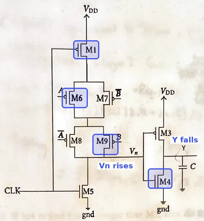
- The edges and the path. In evaluate, B falling turns M9 on and M7 off. For to rise, the upper pair must conduct without M7: A = 0, so M6 is on (and M8 off). rises through M1, M6 and M9 in series, and Y falls through M4.
- Stage 1’s resistance: the series PFETs add. .
- Stage 1’s load: the inverter’s two gates. drives M3 and M4, . Delay .
- Stage 2: M4 alone pulls Y down. .
- Add. Total 35 ps; with the key’s , .
Check. Logical effort gives the same number (Chapter 12, Section 6). . Stage 1: a three-high p stack, , . Stage 2: M4’s balanced inverter is 20/10 µm, so , . . ✓
Answer: 35 ps by , as the chapters compute delays (24.2 ps if you multiply by 0.69, as the key does). Stage 1 is 30 of the 35.
Remember. Count every device between the rail and the node, the clocked header included; series resistances add whatever the internal nodes held. A strength ratio sets a missing width.
The answer key differs
It gives 10.35 “ns”: it counts stage 1 as one PFET (, 6.9 ps with the 0.69) because “the intermediate node is precharged”, and it labels picoseconds as nanoseconds. The charged internal node is why the delay model fits well here; it does not take M1 and M6 out of the path (see the idea above). The key’s stage 2 (3.45 ps with the 0.69) is right.
MT23-3c: the skewed inverter’s noise margins
MT23-3c, p8 (8 points). If M4 is four times stronger than M3, how do the static DC noise margins of this inverter compare with the case the M4 and M3 are sized for equal drive strength? How might this be significant in this circuit?
Hint
What it asks. Two things. First, how the static noise margins of the M3/M4 inverter change when M4 is four times stronger than M3, compared with equal strengths. Second, why that matters “in this circuit”: the inverter’s input is not an ordinary node but , a p-type dynamic node.
The idea. A noise margin runs from where a node sits to where the next gate starts to amplify, the VTC’s −1 points: and (Chapter 6, Section 4). Changing the strength ratio slides the curve sideways and trades one margin for the other; this is MT24-1c’s question with the NFET made stronger instead of the PFET (M3’s noise-margin approach, MT24-1c). The second half is about the node: which margin protects it depends on where it rests and which way noise can push it.
Noise margins and why they matter
- Why the inverter is skewed at all. Y’s falling edge carries the logic ( rises in evaluate), and its rising edge only resets Y during the pre-discharge, which has time. So the inverter after a p node gets the strong NFET (the mirror of Chapter 11, Section 7).
- The curve slides left. The output switches where the NFET’s current matches the PFET’s. A stronger NFET matches the PFET at a smaller input, so the switching threshold moves down, and with it and . and , on the flat ends, barely move.
- The margins follow. shrinks, because its first term fell. grows, because the term it subtracts fell.
- In numbers added. In Chapter 6’s square-law model (, , ; illustrative): equal strengths switch at 2.50 V with ; an NFET four times stronger switches at 2.01 V with and .
- Why it matters here: the node rests at 0 and floats. is a p node. It rests at 0, and when the XNOR is 0 it floats at 0 through the whole evaluate phase, with nothing driving it. Leakage through the off PFETs (Chapter 11, Section 8), charge sharing (Section 10) and coupling can only pull it up, toward the lowered threshold. The margin that protects it is , the one that shrank; and a dynamic node that flips cannot recover until the next pre-discharge.
Check. The mirror of MT24-1c. There a stronger PFET slid the curve right, and grew while shrank. Here a stronger NFET slides it left, so the trade must go the other way, and it does: in the model falls by 0.63 V and rises by 0.84 V.
Answer: is smaller and larger than with equal strengths. It matters because sits at a floating 0 and noise can only push it up: the small is exactly the margin it needs.
Remember. Skewing the inverter toward the logic edge moves its threshold toward the dynamic node’s resting value, and shrinks the margin that protects that value: after a p node, after an n node.
The answer key differs
It states the first part correctly, then ends “With a smaller the noise can switch the inverter”: that should read .
The widget starts with the NFET four times stronger (strength ratio 0.25). Move the ratio to 1 and back, and watch , and the two margins.
MT23-3d: one transistor for the low noise margin
MT23-3d, p9 (6 points). How might the on be improved in this circuit with the addition of a transistor?
Hint
What it asks. One added transistor that improves on : how much noise the resting 0 can take before the inverter misreads it. Part (c) found why it is needed: the node floats at 0 and its margin is small.
The idea. A floating node has no defence: any charge that leaks onto it stays. The cure is to stop it floating, with a weak device that holds the resting value, driven by the inverter’s output so that it turns itself off once the node has really switched. That is Lecture 11’s half latch (Chapter 11, Section 8), drawn there for an n node as a weak PFET to ; a p node needs its mirror. It must be weak, because during a real evaluation the network has to overpower it (Chapter 11, Section 9).
The half latch for a p node
- What is needed. Something that holds at 0 while it should be 0, and lets go when the PFETs really pull it up.
- Mirror Lecture 11’s half latch. For an n node it is a weak PFET from , gated by the inverter’s output. The node here rests at 0 instead of 1, so swap the rail and the device: a weak NFET from to ground, gated by Y.
- At rest it holds. While , Y = 1 and the NFET is on: noise current is drained to ground, and stays at 0.
- In a real evaluation it lets go. The network fights the NFET until passes the inverter’s threshold; then Y falls and turns the NFET off, and the fight ends.
- Keep it weak, because in a real evaluation the PFET network must overpower it before Y can fall and switch it off: about one tenth of the evaluate network’s strength (Chapter 11, Section 9). added Here the worst pull-up path is three 3 µm PFETs, one 1 µm PFET, as strong as a 0.5 µm NFET; a tenth of that is a 0.05 µm NFET, below any minimum width, so it needs a series device or a longer channel.
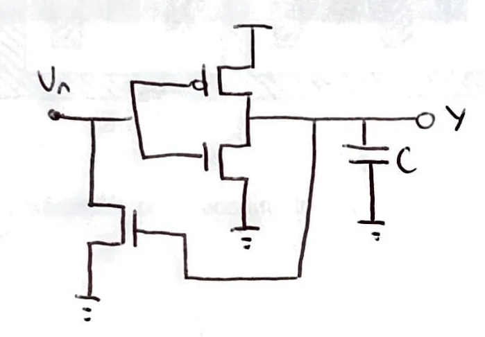
Check. Run the loop through both phases. Pre-discharge: , Y = 1, the NFET is on and only helps M5. Evaluate with the XNOR 0: the NFET keeps holding the 0. Evaluate with the XNOR 1: rises, Y falls, the NFET turns off, and is free to reach . ✓ It never fights a correct result for longer than the switching itself.
Answer: add a weak NFET from to ground, its gate driven by Y: a half latch that holds the resting 0.
Remember. A half latch holds a dynamic node’s resting value, is driven by the node’s own inverter, and is weak. For a p node, everything is mirrored: an NFET to ground.
The answer key agrees
It draws the same circuit (the sketch above).
3. MT17-3c: a footed dynamic stack
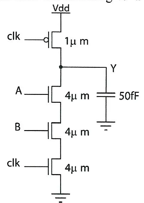
MT17-3, p5–6 (Fall 2017). Consider the following circuits. In each case, please estimate the delays specified as a multiple of the fanout-of-one delay, , for the technology. Assume that the nFET and pFET have the same strength in this problem. [Handwritten addition: assume 2 fF/µm of gate cap.] (c) Calculate the A-rising-to-Y-falling delay in evaluation (clk = 1) for B = 1. (8 points)
Hint
What it asks. The time for Y to fall after A rises, in evaluate (clk = 1) with B already 1, in units of . Two phrases decide the answer: “in evaluation” (so the precharge PFET is off) and, in the stem, “the nFET and pFET have the same strength” (so is the W/W inverter’s FO1 delay). The stem’s handwritten 2 fF/µm turns the 50 fF into gate width.
The idea. The evaluate delay is : the node discharges through the whole evaluate path, the footer included, and the stack rule turns that path into one equivalent device (Chapter 11, Section 4). Then divide by in the page’s convention. The two usual slips are leaving out the footer (Chapter 11 shows it costs 50% here: against ) and using out of habit.
The evaluate delay
- Which devices conduct. In evaluate the 1 µm PFET is off and plays no part. Y falls through A, B and the clocked footer, 4 µm each, in series.
- Why the model fits here. B = 1 and clk = 1 are already on, so the nodes below A are already at ground: A, nearest the output, switches like the top of a stack, the case the model describes well (Chapter 8, Section 10).
- The stack as one device. Three 4 µm devices in series act as one NFET.
- The load in µm of gate, so that it multiplies : .
- in the page’s convention. “Same strength”: the FO1 inverter is W/W, .
- The delay. .
Check. Logical effort gives the same (Chapter 12, Section 2): a three-high n stack at equal strengths has ; A is 4 µm, so , and the gain is . ✓
Answer: (about 9.4). With instead, and the same circuit is : read the convention first.
Remember. Evaluate delay = the whole stack from the node to ground, footer in, precharge device out; then divide by in the question’s strength convention.
The answer key agrees
Check yourself Same circuit, but A = 1 and B rises (clk = 1). Is the delay from B rising larger, smaller or the same as from A rising? What does the course's model give?
Larger. With A on and B off, the node between A and B has been charged from Y through A to about VDD − VT; B must discharge it before Y can fall, and the lecture says the penalty grows roughly as the square of the stack height (Chapter 8, Section 10). The (R/W)C model still gives 9.375 τinv: it describes the device nearest the output and has no term for that internal charge. (MT17-3d asks the same of a NAND4; page M3 solves it.)
4. Extra drill: FN12-8, a domino path
From the Fall 2012 final, adapted as a drill: the midterms have only one domino-sizing problem (MT24-5c). It is re-solved like the rest.
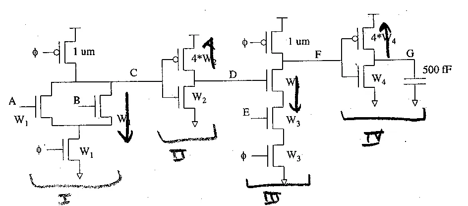
FN12-8, p12–13 (Fall 2012 final, 30 points). Consider the following path of domino logic. The gate capacitance per unit width is 2 fF/µm. The unit width nFET resistance is 4 kΩ, while the unit width pFET resistance is 8 kΩ. Assume that the minimum device width is 0.5 µm. Please ignore source-drain diffusion capacitances and overlap capacitances. (a) Estimate the evaluation delay from A to G if . Assume that (evaluate phase) and that E is high (already evaluated) and B is low. (15 points) (b) Assume that is fixed at 1 µm, but you are free to tune , and . Find approximate values of , and to minimize evaluation delay and estimate the new delay of your resized network. (15 points)
FN12-8a. The evaluation delay (15 points).
Hint
What it asks. The delay from A to G through all four stages in evaluate, with every resizable width at 1 µm, in ns. The conditions pick the path: (evaluate), E already high (so stage III waits only for D), B low (so stage I discharges through A alone). The strengths are 4 and 8 kΩ·µm: .
The idea. A domino path alternates dynamic stages and inverters, and each makes one edge: an n node falls, and the inverter after it rises (Chapter 12, Section 1). Add the stage gains, delay , with in this convention. A dynamic stage’s is for a -high stack, footer counted (Chapter 12, Section 2). The inverters are skewed (PFET 4W over NFET W), and only their rising edge counts, so compare each with the balanced inverter that has the same PFET: 4/2 µm, input 6 µm (Chapter 12, Section 4).
FN12-8a: the evaluation delay
- τ_inv and the load, in the exam’s units. . The load is of gate.
- The logical edges, because they pick the devices: C falls (I), D rises (II), F falls (III), G rises (IV).
- Stage I: A and the footer in series. B is low, so its parallel device doesn’t help. Two 1 µm devices act as 0.5 µm; the reference is ; A is 1 µm: . C drives II’s : , gain 3.33.
- Stage II on its rising edge. Its 4 µm PFET pulls D up; the balanced inverter with that PFET is 4/2 µm (6 µm); its input is 5 µm: . D drives III’s 1 µm D NFET: , gain 0.167.
- Stage III: D, E and the footer, a three-high 1 µm stack: . F drives IV’s 5 µm: gain 5.
- Stage IV, like II: , : gain 41.67.
- Add. Delay .
Check. The big term by : stage IV’s 4 µm PFET is , driving 500 fF, so , and . ✓ It also shows where the time goes: a 1 µm-sized last stage against 500 fF.
Answer: (a) ns.
Remember. In a domino path, mark the edges first: n nodes fall, inverters rise. A skewed inverter’s for its fast edge compares it with the balanced inverter that has the same strong device.
The answer key differs
It adds its own four gains to 50.76 (they add to 50.17), so it gets 1.22 ns. Its gains and its method are right.
FN12-8b. Resizing W2, W3 and W4 (15 points).
Hint
What it asks. Keep at 1 µm, choose , and for the least evaluation delay, and estimate it. Fixing fixes the path’s input; without it, you could make everything huge.
The idea. The equal-gain rule of M4’s MT23-5b applies exactly here. Each inner width is the load of one stage and the size of the next, so it cancels from the product of the gains: is fixed. With a fixed product, the sum is smallest when every gain is the same, : making one stage faster forces another to be slower by a larger factor (Chapter 8, Section 3). This is what MT24-5c lacked: there a fixed branch at X moved ; here nothing sits beside the resized widths.
FN12-8b: resizing W2, W3, W4
- F is fixed, so find it. With fixed, A’s input is 1 µm and the load 250 µm: . . Nothing branches off and every stage keeps its proportions, so whatever – are.
- Equal gains. ; delay .
- Size back from the load, because the last stage’s equation has only one unknown. IV: , so . III: , so . II: , so .
- Stage I checks the work. . ✓ Every width is above the 0.5 µm minimum.
Check. From 1.20 ns to 315 ps, about 3.8 times faster, by resizing alone. A gain of 3.28 per stage is inside the 3–4 that Chapter 8 aims for (Section 4), so four stages are about right for this .
Answer: (b) , , , about 315 ps. FN12-8b is also the second case of the widget in Section 1.
Remember. No branch and nothing fixed beside the resized widths: is fixed, take , size back from the load, and let the first stage check the arithmetic.
The answer key differs
It gives 128.94 for the product of the gains (it is 115.7, or 115.9 with its rounded gains). From it gets 323 ps and , , . Its method is right.
5. Extra drill: FN17-2, two dynamic stages on two clocks
From the Fall 2017 final, adapted as a drill on the race and the collision (Chapter 11, Sections 4–5; Chapter 12, Section 7).
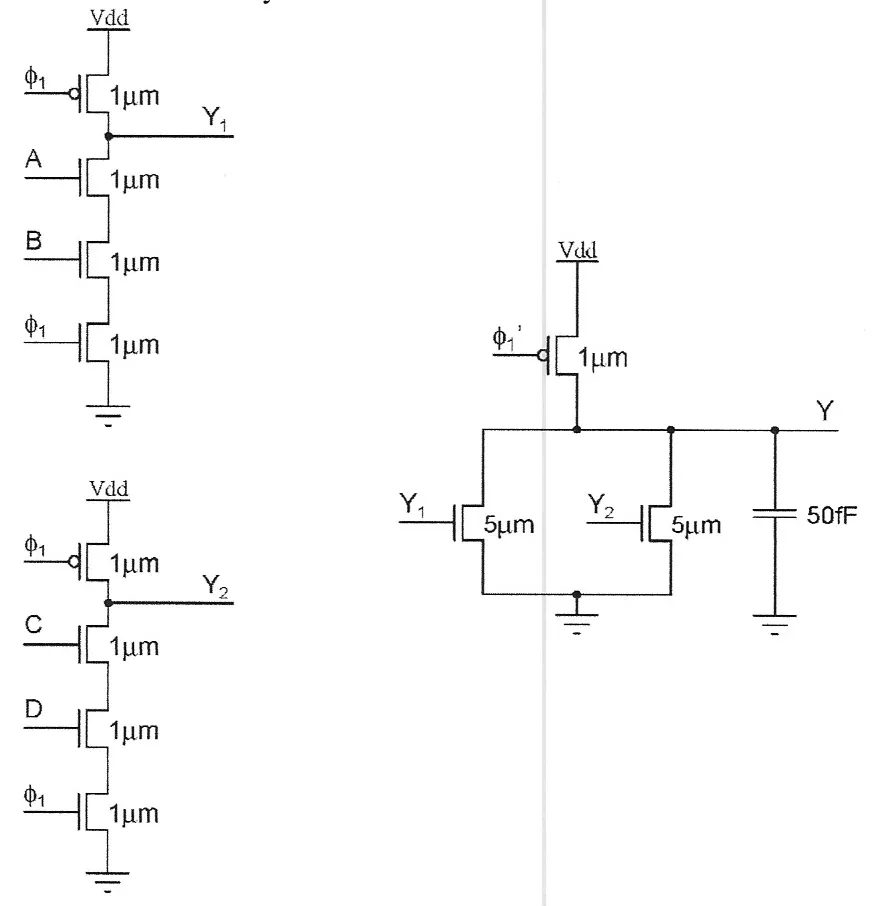
FN17-2, p4–5 (Fall 2017 final, 25 points). Consider the dynamic circuit shown above. Let the fanout-of-one delay of this technology be ps. Let the gate capacitance per unit device width be 2 fF/µm. (a) What relation must the rising edge of have with respect to the rising edge of to avoid a race condition? Explain. Please be precise with calculated delay values. (10 points) (b) What relation must the falling edge of have with respect to the falling edge of to avoid collisions? Explain. Please be precise with calculated delay values. (10 points) (c) With and as chosen in (a) and (b), what logic function does the circuit perform? What is the delay from A rising to Y falling? (5 points)
Two facts in the figure decide every part. The first-stage outputs and are bare dynamic nodes: no inverter follows them, so they sit at 1 at the start of each evaluation and go back to 1 at each precharge. And the second stage has no footer, so nothing stops its NFETs from conducting while it precharges. Like the key, take .
FN17-2a. The race (10 points).
Hint
What it asks. How much later than the clock must rise so that the second stage never evaluates on a wrong input, with the delay computed. “Race condition” names the hazard; “precise with calculated delay values” asks for the first stage’s evaluate delay in ps.
The idea. A dynamic node starts every evaluation at 1, its precharged value. Fed straight into the next dynamic stage, that 1 turns on the next stage’s NFET before the first stage has decided, and whatever charge the second node loses in the meantime is lost for good (Chapter 11, Section 5). Domino cures this with an inverter; this circuit has none, so the second stage has to wait: its evaluation may start only once the first stage’s outputs are final. The wait is the first stage’s evaluate delay, with the footer in the stack.
FN17-2a: the race
- What goes wrong if both clocks rise together. and are precharged to 1, so both second-stage NFETs are on as evaluation starts, and Y begins to discharge even when and are about to fall: the race.
- The rule. The second stage may start evaluating only after the first has finished: rises at least one first-stage evaluate delay after .
- The first stage’s effort. A, B and the footer are three 1 µm NFETs in series, ; the 2:1 reference has input ; A is 1 µm: .
- Its load. drives one 5 µm NFET of the second stage: . (The first stage’s own PFET has its gate on , not on .)
- The delay. .
Check. By : the stack is driving , which is , and with that is . ✓
Answer: must rise at least 500 ps after .
Remember. Two dynamic stages with no inverter between them race. Delay the second stage’s evaluation by the first stage’s evaluate delay, or put an inverter in (domino).
The answer key differs
It says 556 ps: it rounds the stack’s to (); its own method gives , 500 ps.
FN17-2b. The collision (10 points).
Hint
What it asks. How the falling edge of (the second stage’s precharge) must be placed against the falling edge of (the first stage’s) so that the second stage never collides. “Collision” names the hazard, and the second stage’s missing footer is what makes it possible.
The idea. A footless stage collides when its precharge PFET is on while its pull-down conducts: current flows straight from to ground (Chapter 11, Section 4). So it is safe only if its inputs are 0 whenever it precharges. Lecture 12’s delayed reset gets that by letting the second stage precharge a little later, once the first stage’s output has fallen to 0 (Chapter 12, Section 7). That works for domino, where the input comes from an inverter that falls to 0 at precharge. Here the inputs are bare dynamic nodes, which go to 1 at precharge: the rule does the opposite of what it is for. The tempting answer, the key’s, applies it anyway.
FN17-2b: the collision
- When the second stage collides. Its precharge PFET is on () while one of its NFETs is on ( or ).
- What and are. is 1 whenever during evaluation, and always once the first stage precharges (); likewise with C and D.
- Try both orders. If falls before , the second stage collides in every cycle in which or . If it falls after, and have been precharged to 1 by then and the collision is certain.
- Why delayed reset fails here. It works only because a domino inverter’s output falls to 0 when its stage precharges. A bare dynamic node rises to 1.
- So no timing avoids it; change the circuit. The circuit needs a footer on in the second stage; or inverters after the NANDs, and then delayed reset (which changes the function).
Check. Count the safe cases when falls first: the NOR’s pull-down is off only when , that is , one input row in 16. Every other row collides, so no choice of the falling edges can be “safe”.
Answer: with bare dynamic nodes driving a footless stage, no timing of the falling edges avoids the collision; delaying ‘s fall makes it certain. Add a footer to the second stage.
Remember. Delayed reset needs inputs that fall to 0 when their stage precharges, as domino outputs do. A stage fed by bare dynamic nodes needs its footer.
The answer key differs
It says must fall after by the first stage’s precharge time, . The number is the precharge time (a 1 µm PFET driving 5 µm), but the rule is delayed reset, which assumes inverters between the stages; here it guarantees that both NFETs are on when the precharge PFET turns on.
FN17-2c. Function and delay (5 points).
Hint
What it asks. The logic function at Y with the clocks of (a) and (b), and the delay from A rising to Y falling. As in MT24-5b, the named edge pair has to be tested before it is timed.
The idea. Read each node in evaluate: an n node is the complement of its network’s function, so the NANDs give and , and the second stage’s two parallel NFETs make a NOR of them (Chapter 11, Section 4). Then follow the edges: an n node can only fall, so can only fall, and a falling input can only turn an NFET off. The second stage’s own delay is , with a single 5 µm NFET (no footer) as its stack.
FN17-2c: function and delay
- The function. In evaluation , and .
- The edge test. A rising (with B = 1) makes fall, which turns one second-stage NFET off: it can never make Y fall. Y falls only when rises while or is still 1.
- The second stage’s delay. One 5 µm NFET, footless: its 2:1 reference has input 15 µm, so ; Y is : ; .
- Put the two stages together. From rising: the first stage settles in 500 ps, rises then, and a falling Y is done 167 ps later, 667 ps in all. From A rising (B = 1): falls in 500 ps, and Y stays at 1 if .
Check. The second stage by : driving is . ✓ And the function agrees with (b): Y stays high only in the one row of 16 with .
Answer: . A rising cannot make Y fall; Y’s falling evaluation takes 167 ps after rises, 667 ps after rises.
Remember. Before timing an edge pair, check that the circuit can make it: a falling n node only turns NFETs off. In a dynamic circuit, the clock often starts the edge, not the input.
The answer key differs
It gives “from A rising to Y falling”: the same two stage delays (with its 556 ps for 500), on an edge pair that this circuit cannot produce.
Patterns
Dynamic and domino logic (MT17: 5% of the points; MT23: 21%; MT24: 25%).
- Asked every time: the function (8–15 points), a delay along one path (8–15 points), then resizing (MT24, 20 points) or noise and a half latch (MT23, 14 points). The approach section has the moves and why they work.
- Moves: n or p and the evaluate phase; the node as (n) or (p); the one edge each stage makes; the stack from the rail (footer or header in, precharge device out); then or .
- Recurring results: an XOR or a full adder; at equal strengths, (n) and (p) with ; after a p node, shrinks and the half latch is an NFET to ground.
- Traps: an impossible edge (MT24-5b, FN17-2c); a “precharged” node dropping series devices (MT23-3b); the strength convention (MT17-3c); for (MT23-3c); a fixed beside a fixed branch (MT24-5c); delayed reset without inverters (FN17-2b).
- Time: MT24-5 is about 19 minutes (22.5 seconds a point on a 200-point exam), MT23-3 about 16 (30 seconds a point at 150), MT17-3c about 4.
What the keys get wrong
Re-solving every part found these disagreements; all are recorded in this page’s review/decisions.md.
| Part | The key | Here |
|---|---|---|
| MT24-5b | (Sum’s pull-down), 12.875 ns | a falling A makes Sum rise, through W6: , ns |
| MT24-5c | held fixed, , 2.25 ns (, ) | the widths move the branch and ; its widths give 1.53 ns on the falling edge (best about 1.40 ns); on the rising edge is only load (best 6.58 ns) |
| MT23-3b | one PFET in stage 1, 10.35 “ns” | M1, M6 and M9 in series: 35 ps (24.2 ps with 0.69) |
| MT23-3c | “with a smaller ” | (its first sentence is right) |
| FN12-8a | gains sum to 50.76, 1.22 ns | 50.17, 1.20 ns |
| FN12-8b | product 128.94, , 323 ps | 115.7, , 315 ps |
| FN17-2a | 556 ps (1/3 µm rounded to 0.3) | 500 ps |
| FN17-2b | falls 333 ps after | no timing avoids the collision without inverters; that one makes it certain |
| FN17-2c | 723 ps from A rising to Y falling | A rising cannot make Y fall; Y evaluates 167 ps after rises (667 ps after ) |
Every other part (MT24-5a, MT23-3a, MT23-3d, MT17-3c) agrees with its key after re-solving.