FD1. Final practice: adders, shifters and PLAs
This page practises the final’s datapath and control questions: how a fast adder is assembled from small blocks and where its slowest path runs, how a shifter moves a word by any amount in a few rows of multiplexers, and how a PLA turns a truth table into two planes of NOR gates, including the dynamic PLA and the self-timed clocks that keep its planes from racing. Every past-final part on these topics is here, re-solved from the papers; the keys’ answers are not copied, and where a key slips the page says so. The parts come in three families: parallel-prefix adders (FN17-8), logarithmic shifters (FN12-6) and PLAs (FN12-10a, FN19-6a–b). Each family opens with a How to approach section that gives the model and the moves once, and ends with harder added variations: longer chains, setups no past paper uses, and heavier arithmetic, as the real Fall 2026 midterm was.
Every part is worked the same way: what it asks, the idea, why this formula, the solution in steps (each gives its reason first), a check by another route, the answer, and what to remember. Try each part first; open the Hint if you are stuck. The answer key’s verdict is folded at the end of each past-paper part (FN19 has no key; its parts are compared with the unofficial proposed solutions instead).
Before you start. Everything here is taught in Chapter 16, Chapter 17 and Chapter 18, and each section below restates what it uses:
- generate and propagate, the PG cell and the sum (Chapter 16 §9); group terms and the radix-2 element with the carry-in entered as (§12, §13); subtraction with the same adder (§3);
- the element’s order, carries as prefixes, Kogge–Stone, Brent–Kung and the whole prefix adder (Chapter 17 §1–§6); shifts and the logarithmic shifter (§7–§8);
- PLAs as NOR–NOR planes, reading one back, the dynamic PLA and its replica clocks (Chapter 18 §1–§4, §7–§9).
Conventions on this page.
- Positions. As on the Lecture 16 boards and FN17-8, the carry-in is position 0, entered as the pair , and the bits are 1 to , bit 1 the least significant. A span () is the group of positions to , written high index first; the boards and the key write it low index first (“0–8” is the span 8:0).
- Delays. Where a time is needed, the page uses Chapter 17’s example values: the PG cell , one radix-2 element , the sum XOR , for example. Fan-out is ignored, as in the lecture’s level counts.
- Pages are the papers’ printed page labels.
Symbols
| Symbol | Meaning | Unit | First appears |
|---|---|---|---|
| , | bit of the two operands, (bit 1 the least significant) | — | approach 1 |
| the number of bits | — | approach 1 | |
| , | bit ‘s generate and propagate | — | approach 1 |
| , | the adder’s carry-in and carry-out | — | approach 1 |
| a span: positions to , high index first | — | approach 1 | |
| , | a span’s group generate and group propagate | — | approach 1 |
| the radix-2 element: | — | approach 1 | |
| the carry out of bit , ; | — | approach 1 | |
| bit of the sum | — | approach 1 | |
| , , | the delays of the PG cell, one element and the sum XOR | approach 1 | |
| the fan-out-of-one inverter delay (Chapter 7) | ps | approach 1 | |
| , | the depth in elements of (the top sum’s carry) and of () | — | approach 1 |
| bit of the miswired adder’s sum, | — | Variation 1 | |
| the delay of the XOR that inverts for a subtraction | Variation 2 | ||
| , | bit of a shifter’s input and output word, ( the MSB, the sign bit) | — | approach 2 |
| , | the shift amount’s bit (row ‘s select) and the amount, | — | approach 2 |
| bit of the word entering a row of the shifter ( after row ) | — | approach 2 | |
| , , , | FN12-6’s mux: data inputs, control and output, | — | FN12-6 |
| , , | Variation 4’s mode lines and the common pad bit | — | Variation 4 |
| , | a PLA’s input and its complement, each on its own literal line | — | approach 3 |
| a PLA’s AND-plane row (a product term); FN12-10a’s key writes p0–p2 | — | approach 3 | |
| , | a PLA’s outputs (FN12-10a’s with inverters, FN19-6’s without) | — | approach 3 |
| , , | the input clock (clk); the AND plane’s and the OR plane’s clocks (low: precharge, high: evaluate) | — | approach 3 |
| , | the slowest AND row’s (the replica’s) precharge and evaluate times | ps | approach 3 |
| , | the generators’ inverter and NAND delays | ps | FN19-6b |
| the OR plane’s evaluate time | ps | Variation 7 |
How to approach a parallel-prefix adder question
Recognize it by the words: “parallel adder”, “prefix”, “lookahead element”, “radix-two”, “Kogge–Stone”, “Brent–Kung”, “PG generator”, “sum generator”, “critical path”. The paper gives the three blocks’ equations and asks for the block diagram that joins them, and for the slowest path through it. Nothing is computed; the marks are for the wiring and the path.
The model. A sum bit needs the carry into it, and the carry into bit depends on every bit below it. The ripple adder computes those carries one after another, so the last one waits for stages. A prefix adder computes each carry as a group term of all the positions below it, , and builds those groups in a tree of small identical blocks, so the last carry waits only about blocks (Chapter 17 §2). The adder has three rows:
- PG generators at the bottom: each bit makes (it makes a carry by itself) and (it passes an incoming carry on) (Chapter 16 §9).
- The network in the middle: radix-2 elements, each merging two adjacent spans, the higher one on the left (Chapter 17 §1). The carry-in enters at position 0 as : a “group” that generates exactly when and never propagates, because nothing lies below it.
- Sum generators at the top: , each bit’s own propagate XOR the carry into it, which is the carry out of the bit below.
Why these, and their conditions. The three blocks are the paper’s own equations; memorize them (FN17-8 prints them, but the next paper may not). The carries: derive in two lines. The carry out of bit is “a carry made somewhere in positions 0 to and passed by everything above it”, which is the group generate ; the sum of bit needs the carry into bit , which is the carry out of bit . The element is associative, so any bracketing of the same positions in the same order gives the same ; it is not commutative, so the higher span always goes on the left (Chapter 17 §1). The critical path: derive by tracing an output back to the inputs. The top sum needs , not ; needs , which may be a level deeper.
The moves.
- Number the positions: at 0, bits 1 to . Draw them as the paper does (FN17-8’s key puts bit 8 at the left).
- Bottom row: one PG generator per bit.
- The network: Kogge–Stone unless the paper names another. In level , every row whose span does not yet reach 0 merges with the row below it; a row stops once it reaches 0. For 8 bits: 8, 7, 5 and 1 elements, 21 in all, in 4 levels (Chapter 17 §3).
- Top row: from and ; from (straight up from its own PG generator) and the 0-to- output of the bit below it (with bit 8 at the left, the column to its right); from the 0-to- output.
- Critical path: find the depths of and of ; draw PG → elements → top sum, and PG → elements → ; say which is longer and why.
- Check with one addition through the drawing, for example : must come out 1, 0 and 1.
Decide on the way: which network (Kogge–Stone for speed and regular fan-out, Brent–Kung for fewer elements; Chapter 17 §5); whether “critical path” means the top sum or (mark both and say when each wins); which side the carry-in enters (the side of the least significant bit).
Traps. Wiring each sum to its own column’s carry, : one position too high, and the answer key of FN17-8 does it. Swapping an element’s inputs (the lower span on the left). Feeding the sums from the network’s outputs instead of each bit’s own . Forgetting the carry-in, or giving it a propagate of 1. Calling Brent–Kung “faster”: it is smaller, never faster.
FN17-8: an 8-bit parallel-prefix adder and its critical path (15 points)
You need
The PG cell and the sum (Chapter 16 §9). One bit with operands , makes (it generates a carry whatever comes in) and (it passes an incoming carry on). Its carry out is and its sum is .
Groups and the element (Chapter 16 §12, Chapter 17 §1). A run of bits acts like one big bit with a group generate and propagate . Two adjacent groups merge in one radix-2 element, , the higher group on the left. The carry-in is the group at position 0.
Carries are prefixes (Chapter 17 §2). The carry out of bit is , so and . No network of two-input elements can make in fewer than levels.
The question (FN17-8, p18, in the paper’s words). Draw the block schematic diagram of an 8-bit parallel adder composed of an interconnection of three logic building blocks: a PG generator with the equations: , , a radix-two lookahead element with the equations: , , and sum generator with the equation: . Draw the critical path through your network. (15 points)
FN17-8 prints no figure. This is the network its adder is built on: the 8-bit Kogge–Stone network of Lecture 16 (Chapter 17 §3; Lecture16 @ 10:41, redrawn). Each row is a position, the carry-in at the bottom; each element takes its higher input along its row and its lower input on a diagonal from a lower row; row ends in . 21 elements in 4 levels, drawn as the four columns of boxes.
Reading the question. The paper’s lookahead element is written for two bits, , ; in a tree its inputs are groups, so read as the higher span’s and as the lower span’s. The sum generator’s is the carry into the bit. “Your network” leaves the choice of network open: the lecture’s two are Kogge–Stone and Brent–Kung.
The adder and its critical path (15 points)
FN17-8, p18. Draw the block schematic diagram of an 8-bit parallel adder composed of an interconnection of three logic building blocks: a PG generator with the equations: , , a radix-two lookahead element with the equations: , , and sum generator with the equation: . Draw the critical path through your network. (15 points)
Hint
What it asks. A drawing, not a number: the three kinds of block wired into a working 8-bit adder, and the slowest path from an input to an output marked on it. The unknowns are the network between the PG generators and the sum generators, and where each sum takes its carry. The words that decide the method are “radix-two lookahead element”, which says the carries are built in a tree of two-input group merges, and “critical path through your network”, which asks for the deepest chain of blocks.
The idea. Every carry is a prefix: the carry out of bit is the group generate of positions 0 to , with the carry-in as position 0. So the network’s job is to make the eight spans 1:0, 2:0, …, 8:0, and a tree makes them in levels instead of 8. The sums then need only one XOR each, but each must take the carry into its bit, the span that stops one position below it. The critical path is the longest chain PG → elements → output; its length is set by the depth of the carry the output needs.
Why this formula. The adder rests on and .
- Where it comes from. A carry leaves bit if some position generates (position 0 “generates” when ) and every bit from to propagates. That is exactly the group generate of the span , which the element builds by merging adjacent spans (Chapter 17 §2). The sum of bit is its own XOR the carry coming into it, and the carry into bit is the carry out of bit : .
- Why the carry-in is . A group’s carry out is . Below position 0 there is nothing, so its must be 0, and its is itself. Merging any span with it gives : Chapter 16’s group carry.
- Conditions. The element’s inputs must be adjacent spans, the higher one on the left: the element is associative but not commutative (Chapter 17 §1). The propagate must be the XOR, because the sum reuses it.
- The critical-path formula. Each block on a path adds its delay, so the top sum is ready at with the depth of , and at with the depth of .
- The tempting alternative. Taking each sum’s carry from its own column, . It looks tidy (the column ends right under its sum block) and it is wrong: it adds the carry out of the bit back into the bit.
FN17-8
- Positions. Because each carry is a group that reaches down to the carry-in, the network covers nine positions: at position 0 and bits 1 to 8 above it. Following the paper’s key, draw bit 8 at the left and the carry-in entering at the right, so each bit is a vertical line, a column. Turned a quarter turn anticlockwise, the docked network is this grid: its row becomes the key’s column , and its levels, left to right, become the key’s rows of elements, bottom to top.
- Bottom row: eight PG generators. Because the network and the sums both need each bit’s and , bit ‘s generator takes , and gives and .
- Middle: the network. Because Kogge–Stone reaches every carry at the depth bound, use it. Level 1 merges each row with the row below: 1:0, 2:1, 3:2, 4:3, 5:4, 6:5, 7:6, 8:7 (8 elements). Level 2 merges with the row two below: 2:0, 3:0, 4:1, 5:2, 6:3, 7:4, 8:5 (7). Level 3, four below: 4:0, 5:0, 6:0, 7:0, 8:1 (5). Level 4, eight below: 8:0 (1). That is elements in 4 levels; each element’s left input comes along its own row and its lower input on a diagonal from the lower row.
- Top row: eight sum generators. Because needs the carry into bit : , with wired straight up from the input; ; …; . Each sum takes its on a wire straight up from its own PG generator, past the network, and its carry, in the key’s layout, from the top of the column one to its right (the bit below; in the docked network, the end of row ). The 0-to-8 output, , is ; it feeds no sum.
- The depths. Because each level doubles a span’s reach, is ready after 1 level, and after 2, to after 3 and after 4: each at its bound . So for the top sum’s carry , and for .
- The critical path. Because the top sum waits for , one path runs → PG → 7:6 → 7:4 → 7:0 → the XOR: , with the example delays. The other runs → PG → 8:7 → 8:5 → 8:1 → 8:0 → : . Mark both: the sum path is the critical one when the XOR is slower than an element (), the carry-out path otherwise; with the example values they tie.
The FN17-8 answer drawn whole (new figure; the spans come from the drawing’s own taps and the adder is checked on all additions). Each sum takes from its own PG block and its carry from the column one to its right; takes . Thick: the path to the top sum, PG → 7:6 → 7:4 → 7:0 → . Thick dashed: the path to , PG → 8:7 → 8:5 → 8:1 → 8:0. Grey numbers: the levels.
Check. By one addition through the drawing, with : bit 1 has and every other bit . The element 1:0 gives , so ; every span above it meets a killing bit, so . The sums: , , the rest 0: , as it must be. And with , which tests the wire into that never uses: every bit kills, so , and the rest are 0: . The model prefixAdd runs the same drawing on all additions of two 8-bit words and a carry-in and gets every one right. By the bound: no two-input network can make (8 positions) in fewer than 3 levels or (9 positions) in fewer than 4, so this path cannot be shortened by a better network, only by faster blocks.
Answer: Eight PG generators (, ) feed a Kogge–Stone network of 21 radix-2 elements in 4 levels over positions 0 (, 0) to 8, which makes ; eight sum generators make and , and . Critical path: PG → three elements → (), or PG → four elements → (); 18 each with the example delays. (With the board’s Brent–Kung network, 13 elements, is 4 levels deep and PG → four elements → , 22 , is the critical path.)
Remember. Three rows, and one rule for the top row: each sum takes the carry from the bit below, , and is the full span’s output, . The critical path is PG, then the depth of the carry the output needs, then the XOR; the top sum needs , one carry short of .
The key’s drawing (FN17-8, solutions p18)
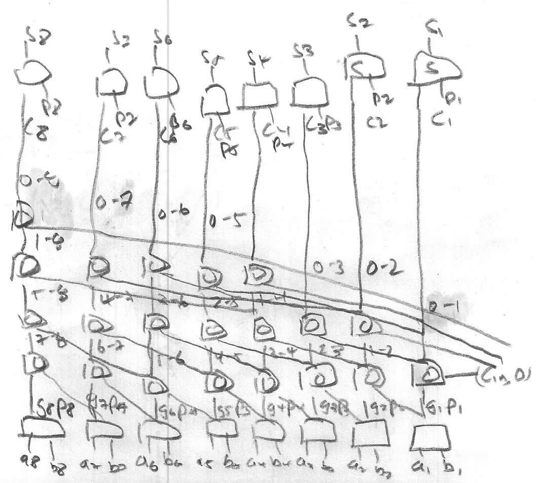
The answer key differs
prefixAdd(…, 'own'), the key’s wiring is wrong on 117,950 (90.0 %); only is always right (Variation 1 finds exactly which additions survive). The fix moves each sum’s carry wire one column to the right and feeds from . Its miswiring also changes the critical path: would wait for , four levels, with the example delays.The key’s slip in one picture (new figure): (a) the right wiring, each from the column one to its right; (b) the key’s, each from its own column (its , †). For with the carries are : (a) gives , (b) gives 01. The key’s wiring is wrong on 117,950 of the additions (Variation 1).
Harder variations: parallel-prefix adders
You need
The prefix adder (Chapter 17 §6). PG generators make , ; a network of radix-2 elements, , makes every carry with at position 0; the sums are and . The top sum is ready at , the depth of ; at .
The two networks (Chapter 17 §3–§5). Kogge–Stone: in level each unfinished row merges with the row below; every carry at the bound . Brent–Kung: power-of-two spans from position 0 first, then the others filled in from them; fewer elements, more levels for some carries.
These three variations added are harder than FN17-8 in the ways the real midterm was: Variation 1 is a debugging chain on the key’s own miswiring, an unfamiliar question form; Variation 2 runs a subtraction through all 21 elements by hand, heavy bookkeeping against the clock; Variation 3 scales the adder to 16 bits and finds that the slowest sum need not be the top one. The budgets assume the practice finals’ pace, about 1.8 minutes a point. No key exists, so there is no key verdict.
Variation 1: debugging the miswired adder (about 20 minutes)
Variation 1: debugging the miswired adder
added The question. An 8-bit Kogge–Stone adder is built as FN17-8’s key draws it: correct PG generators and a correct network, but each sum generator fed from its own column, . (a) Give the smallest addition it gets wrong, and what it outputs. (b) Write in terms of the right sum and two carries. (c) For exactly which inputs is the whole output right? (d) Count them, out of all additions with a carry-in, and give the share. (e) Is ever wrong? A tester applies 100 random additions; how likely is it that every one passes?
Hint
What it asks. A diagnosis of a known fault, in five steps: a failing case, the fault’s algebra, the exact set of inputs that hide it, their number, and what that means for testing. What is unfamiliar is the direction: instead of building the adder, the question asks what a specific wrong one does.
The idea. The miswired sum uses the carry out of its bit where it should use the carry into it. XOR is its own inverse, so the error in bit is the XOR of those two carries: the output is right in bit exactly when the carry does not change across bit . All eight bits are right only when no carry changes anywhere, so every carry equals , and that is a condition on each bit separately, which makes the count a simple power.
Why this formula. .
- Where it comes from. XOR is associative and , so inserting it changes nothing; the first bracket is the right sum (Chapter 17 §6).
- Conditions. Only the sum wiring differs; the PG generators and the network are right, so every is the true carry.
- When a carry does not change across bit . . If the carry stays 0 unless the bit generates (); if it stays 1 unless the bit kills ().
- The tempting alternative. Counting the cases where the sum happens to be right by testing a few numbers. The exhaustive count follows from the algebra in two lines and is exact.
Variation 1
- (a) The smallest failure. Because the error appears where a carry changes across a bit, look for the smallest addition in which one does. With it happens at once: in bit 1 kills, so while , and the miswired adder gives and every other bit 0: it outputs 0 for . With a carry can change only where a bit generates, so the smallest case is : while , and : it outputs for .
- (b) The error term. Because and share , : bit is wrong exactly when the carry into it differs from the carry out of it.
- (c) When all eight bits are right. Because each bit needs , the whole word is right only when : every carry equals . With that means no bit generates (each ); with , no bit kills (each ).
- (d) The count. Because the condition is on each bit alone, each bit has 3 allowed pairs out of 4: cases with and with , right. Wrong: . The share right is .
- (e) The carry-out, and a test. Because comes straight from the network, which is right, is never wrong; only the sum bits are. A random addition passes with probability , so all 100 pass with probability , about : the first test or two will catch it.
Check. By the model: countWrong on the key’s wiring finds 117,950 wrong additions, and running all cases confirms that the output is right exactly when every carry equals , and that always agrees. At 4 bits the same formula gives wrong, the count Chapter 17 §6 gives for its 4-bit adder.
Answer: (a) with gives 0 instead of 1; with , the smallest is , which gives 1 instead of 2. (b) . (c) Right only when every carry equals : no bit with if , no bit with if . (d) right, 117,950 wrong; right. (e) is always right; 100 random tests all pass with probability about .
Remember. An off-by-one carry corrupts a sum bit exactly where the carry changes: the error is . A wiring fault that only shows when a carry moves survives the additions with no carries at all, such as with or any two numbers with no common 1 bits.
Variation 2: a subtraction through all 21 elements (about 25 minutes)
Variation 2: a subtraction through all 21 elements
added The question. FN17-8’s Kogge–Stone adder is made a subtractor as in Chapter 16 §3: each passes through an XOR with the subtract line, which inverts it, and . (a) For and , write and in binary and the nine leaf pairs , included. (b) Evaluate all 21 elements, level by level. (c) Read off the carries and the result; what does say? (d) What would FN17-8’s key wiring output for the same subtraction? (e) Repeat (c) for and interpret the result. (f) With the XOR taking (for example), when is ready?
Hint
What it asks. A full hand evaluation of the network, as an exam might ask to “show the values on your diagram”: 9 leaves, 21 elements, 8 sums, then an interpretation. The arithmetic is light per element but long, and one slip propagates; that is the time pressure.
The idea. Two’s complement turns subtraction into addition: , so , and the is the carry-in (Chapter 16 §3). Then everything is FN17-8’s adder. Each element needs only three facts: a high span that generates gives ; one that kills, , gives ; one that propagates, , passes the low span through unchanged.
Why this formula. , read as three cases.
- Where it comes from. The element’s equations (Chapter 17 §1). With the output is ; with it is ; with it is . never occurs.
- Conditions. The higher span on the left; spans adjacent. The carry-in pair is here, a generating position 0.
- What means. , so the carry out of bit 8 is 1 exactly when : no borrow.
Variation 2
- (a) The leaves. Because bit 1 is the least significant: , , . Bits 1 to 8 (from the right): gives 0, 0, 1, 1, 0, 1, 1, 0 and gives 1, 1, 1, 0, 0, 0, 1, 1. So = bit 1 , bit 2 , bit 3 , bit 4 , bit 5 , bit 6 , bit 7 , bit 8 , and position 0 is .
- (b) Level 1 (each row with the row below). Because level 1 joins each row to the one below, each element sees two single positions: 1:0 = ; 2:1 = ; 3:2 = (bit 3 generates); 4:3 = ; 5:4 = (bit 5 kills); 6:5 = ; 7:6 = ; 8:7 = .
- (b) Level 2 (two rows below). Because level 2 joins each row to the span two rows below, its inputs are level 1’s outputs (or the carry-in and 1:0, passed along their rows): 2:0 = 2:1 ∘ = ; 3:0 = 3:2 ∘ 1:0 = ; 4:1 = 4:3 ∘ 2:1 = ; 5:2 = 5:4 ∘ 3:2 = ; 6:3 = 6:5 ∘ 4:3 = ; 7:4 = 7:6 ∘ 5:4 = ; 8:5 = 8:7 ∘ 6:5 = .
- (b) Levels 3 and 4 (four, then eight rows below). Because each level doubles the reach, level 3 finishes rows 4 to 7 and level 4 finishes row 8: 4:0 = 4:1 ∘ = ; 5:0 = 5:2 ∘ 1:0 = ; 6:0 = 6:3 ∘ 2:0 = ; 7:0 = 7:4 ∘ 3:0 = ; 8:1 = 8:5 ∘ 4:1 = . Then 8:0 = 8:1 ∘ = .
- (c) Carries and sums. Because is the of the span : = 1, 1, 1, 1, 1, 0, 0, 1, 1. The sums , bits 1 to 8: , , , , , , , . Read from bit 8 down: , and : no borrow, .
- (d) The key’s wiring. Because it XORs each with instead: bits 1 to 8 give , , , , , , , = 0, 0, 1, 0, 0, 1, 1, 0, so . The carry changes across bits 5 and 7, and exactly those bits are wrong (Variation 1).
- (e) The other way round. Because only the inverted operand changes, the same network runs again: : , and the same network gives carries 1, 1, 1, 0, 0, 1, 1, 0, 0, and . A carry-out of 0 is a borrow: the result is negative, in two’s complement.
- (f) The time. Because the XOR on sits in front of the PG generators and the path is otherwise FN17-8’s: .
Variation 2 through the network (computed in checks.test.ts and in the figure’s generator): , each node labelled . The carries at the top, = 1, 1, 0, 0, 1, 1, 1, 1, 1, give with dropped.
Check. By the integers: , so the sum is 52 with a carry out of 1; and , so no carry out. By a ripple of the carries, bit by bit: ; bits 1 and 2 propagate it (1, 1); bit 3 generates (1); bit 4 propagates (1); bit 5 kills (0); bit 6 propagates the 0 (0); bit 7 generates (1); bit 8 propagates (1). The same nine carries as the tree.
Answer: (a) ; bits 1–8: , , , , , , , . (b) Level 1: 1:0 , 2:1 , 3:2 , 4:3 , 5:4 , 6:5 , 7:6 , 8:7 ; level 2: 2:0, 3:0, 4:1 , 5:2, 6:3 , 7:4, 8:5 ; level 3: 4:0 , 5:0, 6:0 , 7:0, 8:1 ; level 4: 8:0 . (c) Carries 1, 1, 1, 1, 1, 0, 0, 1, 1; , (no borrow). (d) 100. (e) , : a borrow, . (f) .
Remember. A subtractor is the adder with and , and means “no borrow”. To evaluate a network fast, classify each span as generate , kill or propagate : a generate or kill on the left decides the element alone; a propagate passes the right input through.
Variation 3: sixteen bits, and the sum that comes last (about 20 minutes)
Variation 3: sixteen bits, and the sum that comes last
added The question. A 16-bit prefix adder with a carry-in (positions 0 to 16). (a) How many elements and levels does Kogge–Stone need? (b) The strict Brent–Kung pattern over the same 17 positions has 27 elements and 6 levels, with carry depths 1, 2, 2, 3, 3, 4, 3, 4, 4, 5, 4, 5, 5, 6, 4, 5 for to . Which carries are deepest, and why is shallow? (c) With the example delays, when is each adder’s top sum ready, and its ? (d) Which sum is the last to be ready in each adder, and when? (e) Name the critical path of the Brent–Kung adder, block by block.
Hint
What it asks. The same adder at twice the width, in both networks, and a comparison that goes beyond : which output really finishes last. The unfamiliar step is (d): FN17-8’s rule of thumb, “the top sum or ”, fails for Brent–Kung.
The idea. Kogge–Stone puts every carry at its bound, so its deepest carries are the highest ones, and the top sum and are the last outputs. Brent–Kung’s up-sweep builds the power-of-two spans from position 0 directly: 1:0, 3:0, 7:0 and 15:0, at levels 1 to 4. The other carries are filled in afterwards, each one element after a carry it builds on, and those fill-ins can be deeper than the top ones. The critical path ends at the sum whose carry is deepest, wherever it sits.
Why this formula. , the depth of the carry each sum needs, maximized over .
- Where it comes from. The critical-path formula of FN17-8, applied to every sum instead of only the top one. FN17-8’s version assumes the deepest carry below is , which holds for Kogge–Stone and fails for Brent–Kung.
- Kogge–Stone counts. Level has elements over positions (Chapter 17 §3); levels .
- Conditions. One delay per element, fan-out ignored (Brent–Kung’s heavily loaded nodes would make it slower still).
Variation 3
- (a) Kogge–Stone. Because level merges rows apart and 17 positions need 5 doublings (): elements, 5 levels. to are at their bounds: 1, 2, 2, 3, 3, 3, 3, then 4 for to , and 5 for .
- (b) Brent–Kung’s deep and shallow carries. Because the up-sweep pairs and doubles from position 0, it makes , , , (spans 1:0, 3:0, 7:0, 15:0) at levels 1, 2, 3, 4, the bound. The down-sweep then makes 11:0 from 11:8 and 7:0 (level 4), 13:0 from 13:12 and 11:0 (level 5), and 14:0 from bit 14 and 13:0 (level 6). So is the deepest carry, at 6; , , and are at 5. Half the elements of Kogge–Stone (27 against 54) cost one more level.
- (c) Top sum and carry-out. Because needs : Kogge–Stone , Brent–Kung the same 22, since is an up-sweep carry at level 4. is at level 5 in both: .
- (d) The last sum. Because each waits for : in Kogge–Stone the deepest carry below is at level 4, so to all finish at . In Brent–Kung, needs at level 6: , eight later than its top sum.
- (e) Brent–Kung’s critical path. Because is built on the longest chain of the network, the up-sweep to 7:0 and then three fill-ins: → PG → 1:0 → 3:0 → 7:0 → 11:0 → 13:0 → 14:0 → the XOR. Each element on it takes the previous one as its lower input (3:0 = 3:2 ∘ 1:0, 7:0 = 7:4 ∘ 3:0, 11:0 = 11:8 ∘ 7:0, 13:0 = 13:12 ∘ 11:0, 14:0 = bit 14 ∘ 13:0). Block by block: PG, six elements, XOR.
Carry depths for 16 bits (computed from the two networks over 17 positions; solid Kogge–Stone, hatched Brent–Kung). Brent–Kung’s is the deepest carry (6 levels), while , made by the up-sweep, is ready after 4.
Check. By the bound: spans 15 positions, so any two-input network needs at least levels; Brent–Kung’s 6 is two over, which matches Chapter 17 §5’s Brent–Kung levels against Kogge–Stone’s : they differ by at . The model prefixAdd runs both networks on 3000 random 16-bit additions each and gets every one right, so the depths belong to working adders; analyse gives 54 and 27 elements, 5 and 6 levels.
Answer: (a) 54 elements, 5 levels. (b) is deepest (6 levels); is made by the up-sweep at level 4, the bound. (c) at and at in both. (d) Kogge–Stone: to at 22; Brent–Kung: at . (e) PG → 1:0 → 3:0 → 7:0 → 11:0 → 13:0 → 14:0 → the XOR: PG, six elements, the sum XOR.
Remember. The critical path ends at the sum whose carry is deepest. In Kogge–Stone that is the top sum (or ); in Brent–Kung it can be a sum in the middle, because the up-sweep’s power-of-two carries arrive early and the filled-in ones late.
How to approach a logarithmic shifter question
Recognize it by the words “shifter”, “shift amount”, “arithmetic right”, “logical”, “rotate”, a multiplexer block with its equation (FN12-6 prints ), and “a three-bit control signal”. The paper asks for a block-level schematic; the marks are for the rows, the wiring of each mux’s two inputs, and what fills the vacated end.
The model. A right shift by places makes output bit equal to input bit ; the top outputs have no input bit to copy and must be filled: with 0 for a logical shift, with copies of the sign bit for an arithmetic one, with the bits that fell off the bottom for a rotate (Chapter 17 §7). Any amount from 0 to is a sum of distinct powers of 2, so a shift by is a shift by 1 or not, then by 2 or not, then by 4 or not, each controlled by one bit of written in binary. Each conditional shift is one row of 2:1 multiplexers (Chapter 17 §8).
Why these, and their conditions. is the word entering the row. The shift amounts of the rows add, because shifting by and then by is shifting by ; derive the structure from that. The pad count is : row has muxes whose shifted input would come from beyond the MSB. For an arithmetic shift every pad is , taken straight from the input: an arithmetic right shift never changes the MSB, so every row’s MSB is still . The stack height counts the driver plus one pass device per row, if the muxes are pass transistors (Chapter 17 §8); derive it, and break it with inverters every two or three rows, inverting the pads of the rows that carry inverted data.
The moves.
- Read the mux equation: which input passes when the control is 1. In FN12-6, : passes when .
- One row per select bit, shifting by 1, by 2, by 4 (any order works; keep the paper’s).
- In row , mux : the control is ; the selected-when-1 input takes the bit to the left (index ) of the row above; the other takes the bit straight above.
- The pads: every 1-input whose index passes : tie it to 0, or the wrapped bit, as the shift kind demands.
- Count the muxes and pads, and check one word through the rows, for example a negative number shifted by an amount with two 1 bits.
Decide on the way: the shift kind (the pads); whether the paper wants transistor detail (pass muxes, stack height, inverters) or only blocks; which input of the paper’s mux is the selected-when-1 one.
Traps. Swapping the mux inputs (then shifts by 7). Padding an arithmetic shift with 0. Taking a pad from the row’s own output on the wrong side. Inserting inverters but leaving the next rows’ pads uninverted. Using a one-hot select (eight lines) where the paper says “a three-bit control signal”: that is the barrel shifter.
FN12-6: an 8-bit arithmetic right shifter from 2:1 muxes (15 points)
You need
Shifts (Chapter 17 §7). A right shift by moves every bit places toward the LSB. A logical shift fills the vacated top bits with 0; an arithmetic shift fills them with copies of the MSB (sign extension), so that a two’s-complement number is divided by , rounding down: .
The 2:1 multiplexer (Chapter 17 §8). A select picks one of two inputs. Built from pass transistors it is two NFETs (or two transmission gates) joined at the output, so a signal passing through several in a row sees them in series with its driver: the stack height.
Two’s complement (Chapter 15 §11). The MSB of an 8-bit word weighs : .
The question (FN12-6, p7, in the paper’s words). Draw the (block-level) schematic of an 8-bit arithmetic right shifter using the basic multiplexer building block shown below. The shift amount should be determined by a three-bit control signal. (15 points)
FN12-6’s building block (Final 2012, p7, redrawn): a 2:1 multiplexer with data inputs and , control and output , so when and when .
The exam’s own figure (FN12-6, p7)
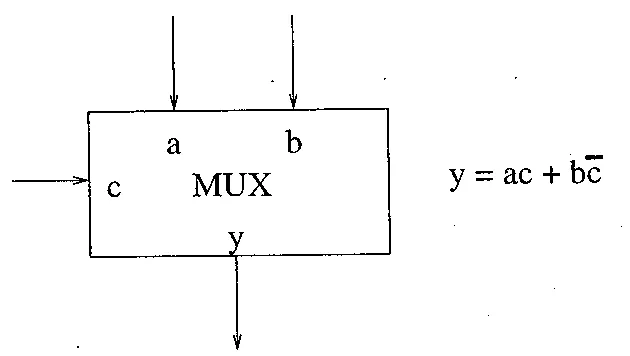
Reading the question. “Arithmetic right” fixes the fill: copies of the sign bit . “A three-bit control signal” fixes the select: the shift amount in binary, , which is the logarithmic shifter, not the barrel shifter (whose eight selects are one-hot).
The shifter (15 points)
FN12-6, p7. Draw the (block-level) schematic of an 8-bit arithmetic right shifter using the basic multiplexer building block shown below. The shift amount should be determined by a three-bit control signal. (15 points)
Hint
What it asks. A block diagram: an 8-bit word in, the word shifted right arithmetically by out, built only from the paper’s 2:1 mux, with given as three bits. The unknowns are how many muxes, how they are arranged and wired, and what feeds the inputs that have no bit to take. The decisive words are “three-bit control”, which says each control bit must act on its own, and “arithmetic”, which says what fills the top.
The idea. Write the amount in binary, . A shift by is then a shift by 1 if , followed by a shift by 2 if , followed by a shift by 4 if . Each of those is a row of eight muxes all controlled by one select bit: each mux passes either the bit straight above (no shift) or the bit places to the left (shift). Three rows, eight muxes each. The muxes near the top have no bit to their left; for an arithmetic shift they take the sign bit , so that the vacated places fill with copies of the sign.
Why this formula. Row , mux : with (or if ) and , where is the word entering the row.
- Where it comes from. The paper’s equation, , passes when . With , the row shifts when its select bit is 1, so must be the shifted bit and the unshifted one. Shifts compose by adding, so three rows give every amount (Chapter 17 §8).
- Why every pad is . The vacated bits of an arithmetic right shift are copies of the MSB. After any row the MSB is still (the row copied it into place 7 or left it there), so the pads of every row can come straight from the input ; that also avoids a wire from one row’s output back to its own pad.
- Conditions. The rows are independent and in any order; the paper’s must be driven by one bit of the amount per row.
- The tempting alternatives. Padding with 0 (a logical shift: by 6 would give 2, not ). Swapping and (then shifts by 7). One row of 8:1 multiplexers per bit (eight-input selection that the paper’s 2:1 block does not offer).
FN12-6
- The select. Because the amount is three bits, write : controls a shift by 1, by 2, by 4.
- Row (by 1). Because each output bit must become when and stay when : eight muxes, each with , , . Mux 7’s would be , which does not exist: tie it to . Call the row’s outputs .
- Row (by 2). Because the same logic applies two places at a time: mux has , , . Muxes 7 and 6 would need and : tie both inputs to .
- Row (by 4). Because the last select bit shifts four places at a time, mux has , , ; muxes 7, 6, 5 and 4 take . The row’s outputs are .
- Count. Because there is one row per select bit and one mux per output bit: muxes, and pad inputs, all wired to .
- One word through it. Because a negative number with two select bits set exercises the pads of two rows: (), (shift by 6). Row = 0 passes it: . Row = 1 shifts by 2 and pads with : . Row = 1 shifts by 4 and pads with 1: .
The FN12-6 answer drawn (new figure; the drawn wiring is checked on all 256 words and 8 amounts): 24 of the paper’s muxes, selected when the row’s select is 1. Row ‘s mux takes from straight above and from columns to the left; the 7 pads past bit 7 hang on the rail at the left. At the right, Step 6’s word shifted by row by row.
Check. By value: , which is , the output of step 6. With 0 pads the same circuit would give , which is for the unsigned reading: the pads alone make it arithmetic. The model logShifter(…, true) runs the drawn shifter on all words and amounts and matches every time.
Answer: A logarithmic shifter: three rows of eight muxes (24 in all). Row () is controlled by and shifts by : mux has , = the row input’s bit , = its bit . The seven inputs with (mux 7 in row ; 7, 6 in row ; 7, 6, 5, 4 in row ) are tied to , the sign bit.
Remember. Shift amount in binary → one row per bit, row shifting by ; the mux input that passes on a 1 takes the shifted bit; the pads say which kind of shift it is: 0, the sign bit , or the wrapped bit.
The key’s drawing (FN12-6, p7)
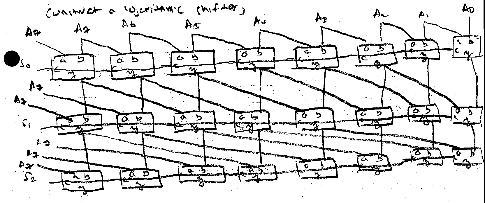
The answer key agrees
Harder variations: logarithmic shifters
You need
The logarithmic right shifter (Chapter 17 §8). rows of 2:1 muxes; row , controlled by , passes either the bit straight above or the bit to the left, so the rows together shift by . The inputs that would reach past the MSB are pads: 0 (logical), (arithmetic), or the bit that fell off the bottom (rotate).
Stack height (Chapter 17 §8). With pass-transistor muxes, a path is its driver plus one pass device per row it crosses, in all; an inverter after a row starts a new stack, inverts the data, and so inverts what the following rows’ pads must carry.
The barrel shifter (Chapter 17 §9). One NFET for every (output, shift amount) pair, devices, with one-hot selects.
These two variations added go beyond FN12-6 in the ways the real midterm did: Variation 4 adds a mode the paper never asks for (rotate) and asks for the extra hardware and its cost in stack height; Variation 5 scales to 32 bits and makes the reader place buffers and work out each row’s pad polarity, a chain of five dependent parts. Budgets assume about 1.8 minutes a point. No key exists.
Variation 4: one shifter, three kinds of shift (about 25 minutes)
Variation 4: one shifter, three kinds of shift
added The question. FN12-6’s 8-bit right shifter, built from the paper’s 2:1 mux, must now do a logical, an arithmetic or a rotating right shift, chosen by two mode lines: (1 for rotate) and (1 for arithmetic, used only when ). (a) What must each pad input carry in each mode? (b) Add the fewest blocks: what goes on each pad, and how many 2:1 muxes in all? (c) Shift by in all three modes, row by row. (d) Check each result by value. (e) With pass-transistor muxes and the fill made by one static gate, what is the worst stack height now, and on which path?
Hint
What it asks. A small design extension and its cost: the pad logic for three modes, the block count, one word worked in three modes, and the effect on the stack. The unfamiliar part is the rotate: its pads come from the bottom of the same row, not from a fixed bit.
The idea. Only the pads differ between the three shifts; the 24 row muxes stay. A logical shift pads 0, an arithmetic one , and a rotate pads each row with the bits that row pushes out at the bottom: in row the mux at needs , the input bit . So each pad is a choice between “the wrapped bit” and “a fill bit”, and the fill bit is , the same for every pad. A choice between two signals is exactly the paper’s mux.
Why this formula. Pad of row , mux (): , with .
- Where it comes from. A rotate right by makes ; rotations compose like shifts, so each row can rotate by or not, wrapping the bits it pushes out (Chapter 17 §7). The fill is FN12-6’s when and 0 otherwise.
- The fill from the paper’s block. with , , gives : one more mux. Made instead as one static AND gate, it restores the level, which matters for (e).
- Conditions. is ignored when . Each bit wraps at most once in a whole rotation, because the total amount is below 8.
Variation 4
- (a) The pads by mode. Because only the vacated places differ: logical 0, arithmetic , rotate the wrapped bit of the same row’s input (row mux 7 takes ; row muxes 7, 6 take , ; row muxes 7 to 4 take to ).
- (b) The added blocks. Because each of the 7 pads chooses between its wrapped bit and the common fill, put one paper mux on each pad: , , ; and one more mux makes (, , ). In all muxes.
- (c) Logical, , (by 3). Because and , rows and shift, row passes, and the pads are 0. Row (by 1, pad 0): . Row (by 2, pads 0): . Row = 0: .
- (c) Arithmetic (pads ). Because only the pads change with the mode, the rows are the same with 1s entering at the top. Row : . Row : . Row = 0: .
- (c) Rotate (pads wrapped). Because each row’s pads take the bits that row pushes out at the bottom: row : the 0 leaving bit 0 enters bit 7: . Row : the 1, 1 leaving bits 1 and 0 enter bits 7 and 6: . Row = 0: .
- (e) The stack. Because a pad path now has the pad mux in it: a wrapped bit passes its driver, the pad mux and the three rows (one pass device per row, whether it shifts or not): 5. The fill path is the same length if the fill comes from a static gate (gate, pad mux, three rows); made by the paper’s pass mux instead, it would be 6. FN12-6’s shifter had 4.
Variation 4’s row (new figure; checked in all three modes on 256 words): each pad of the row is a pad mux with , choosing the wrapped bit ( for mux 7, for mux 6) or the common from one AND gate.
Check. (d) By value, unsigned, signed. Logical: . Arithmetic: . Rotate: the three bits that fall off, 110, re-enter at the top: . A simulation of the drawn circuit (row muxes, pad muxes and fill) matches the three shifts on all words and amounts in each mode, and its worst path is 5 devices.
Answer: (a) Logical 0; arithmetic ; rotate the bit the same row pushes out at the bottom, . (b) One mux per pad (, = the wrapped bit, ) and one for : 32 muxes. (c) Logical , arithmetic , rotate . (d) 18, , 210. (e) 5 (driver, pad mux, three rows), against 4 for FN12-6’s shifter; 6 if the fill is a pass mux too.
Remember. The rows of a logarithmic shifter never change; the kind of shift lives entirely in the pads. Extra logic on the pads lengthens exactly the paths that use them, so make the shared fill with a restoring gate.
Variation 5: thirty-two bits, buffered (about 25 minutes)
Variation 5: thirty-two bits, buffered
added The question. A 32-bit arithmetic right logarithmic shifter, its muxes made of pass transistors. (a) How many rows, muxes and pads, and how many select bits? (b) What is a path’s stack height with no buffers? (c) Place the fewest inverters (one after every mux of a row) that keep every stack at 3 or less; which rows? Does the output come out true or inverted? (d) What must the pads of each row carry? (e) Compare the device count with a 32-bit barrel shifter’s.
Hint
What it asks. The same structure at four times the width, then the transistor-level fixes FN12-6 leaves out: buffering, the polarity of the data after the buffers, and what that does to the sign-bit pads. The chain matters: (d) depends on (c).
The idea. 32 bits need 5 select bits, so 5 rows; a path crosses all 5, so with its driver the stack is 6. Each inverter starts a new stack, so at most two rows can follow a driver: inverters after rows and give stacks of 3, 3 and 2. Each inverter also flips the data, so rows and carry inverted bits; a pad in those rows stands for an inverted bit too, so it must be . After the second inverter the data is true again.
Why this formula. Stack height ; rows ; pads .
- Where it comes from. The board’s count, “my stack height here is at least four” for 8 bits (Chapter 17 §8): the driver and one pass device per row. An inverter after a row is a new driver.
- Pads after an inversion. A row passes what it is given; if its data are inverted, a pad that must stand for the sign bit must also be inverted, as the lecture says of the 8-bit case: “I would need to also invert these zeros” (Lecture16 @ 32:12).
- Conditions. Each inverter sits after every mux of its row; the pads come from the input (or its complement).
Variation 5
- (a) Size. Because each row handles one select bit and shifts by : rows (, shifts 1, 2, 4, 8, 16) of 32 muxes: 160 muxes. Pads: row has , so .
- (b) Unbuffered. Because a bit crosses one pass device in each of the 5 rows after its driver: , far past 3.
- (c) Buffers. Because each driver can be followed by at most two pass devices, five rows need two inverter rows (one inverter after would leave 4 and 3), and any two that leave no more than two pass rows per stack work. Three placements do: after and (stacks 2, 3, 3), after and (3, 2, 3), and after and (3, 3, 2). Take the last: driver + + = 3, inverter + + = 3, inverter + = 2. Two inversions cancel, so the output is true in all three.
- (d) The pads. Because rows and see true data, their 3 pads are ; rows and see the data inverted by the first inverter, so their pads are ; row , after the second inverter, sees true data again: its 16 pads are . For the other placements the inverted-pad rows are and (inverters after and ) or alone (after and ).
- (e) Against the barrel shifter. Because the barrel shifter joins every output to every shift amount by one NFET: NFETs, plus a 5-to-32 decoder for one-hot selects. The log shifter’s 160 pass-NFET muxes use NFETs plus the 64 inverters of two rows. The mux NFETs alone are 3.2 times fewer; with the inverters, 448 devices, under half; but more series stages.
Variation 5’s 32-bit shifter in bands (new figure; stacks from logStackHeights(5, [1, 3])): inverter rows after and cap every series stack at 3 (a driver and two pass devices). Between the two inverter rows the data is complemented, so rows and pad with ; the output is true again.
Check. By the extreme case: () shifted by 31 must give , all ones. With every row shifts and pads; the simulation with inverted pads in rows , gives , and on 4000 random words and amounts it matches the arithmetic shift every time. With on every pad instead, shifted by 4 does not come out : the wrong polarity in row puts zeros into a negative number.
Answer: (a) 5 rows, 160 muxes, 31 pads, 5 select bits. (b) 6. (c) Two inverter rows, after and (stacks 3, 3, 2), after and (2, 3, 3) or after and (3, 2, 3); output true. (d) For , : rows , , take (19 pads), rows , take (12 pads); for , : rows , take ; for , : row alone. (e) Barrel 1024 NFETs; log shifter 320 NFETs in its muxes, about 3.2 times fewer.
Remember. Buffering a pass-transistor shifter is a parity bookkeeping job: count the inverters above each row, and invert that row’s pads when the count is odd. Place buffers every two rows to keep stacks at 3.
How to approach a PLA question
Recognize it by the picture: a grid of vertical literal lines ( and , often with ground lines between them), horizontal rows with a pull-up at one end, small NFETs at some crossings, and a second grid of columns at the right; or by the words “PLA”, “AND plane”, “OR plane”, “product terms”, "", "", “replica”. The papers ask three things: read the functions off a drawn PLA (FN12-10a, FN19-6a), build one, or clock a dynamic one (FN19-6b).
The model. A PLA builds any sum of products from NOR gates only (Chapter 18 §1). Each row of the AND plane is a NOR of the literal lines its devices sit on: a device whose gate is on line pulls the row low when , so the row is high only when every one of its lines is 0. By De Morgan that NOR is the AND of the complements, a product term. Each column of the OR plane is a NOR of the rows it has devices on, so with an inverter after it, it is their OR. In a static PLA the gates are pseudo-NMOS: a PFET load with its gate grounded (Chapter 18 §2). In a dynamic PLA each plane is precharged high while its clock is low and evaluates while it is high, and the OR plane must wait for the AND plane (Chapter 18 §7).
Why these, and their conditions. A device on line means the row needs , and a device on means it needs : the flip is the whole trick of reading, and it comes from the NOR (derive: NOR of lines = AND of their complements). The output inverter decides between the OR of the rows and its complement; FN19-6 draws none. The clock requirements come from the race: during precharge every row is high, so if the OR plane evaluated while a row was still falling, that row’s device would discharge its column for good (Chapter 18 §7); memorize them in words. A replica row tracks the real rows at every process, voltage and temperature corner because it is one (Chapter 18 §8–§9).
The moves.
- Label the lines at the bottom of each vertical: true, complement and ground. Note which way each device’s gate faces.
- Each row: list its devices’ lines, flip each literal, AND them.
- Each column: the rows with devices in it; OR them, and complement if there is no output inverter.
- Simplify (absorption ; ), then check two input rows by tracing them through the grid, not through the formula.
- For a dynamic PLA: state the clock order (the AND plane evaluates first), and build the clocks from replica rows: the slowest precharge (the most capacitance on the row) for ‘s low pulse, the slowest evaluate (one device on) for ‘s rising edge.
Decide on the way: output inverters or not; which literal a device’s gate is on (the lines alternate , ground, ); whether “simplify” is wanted (FN12-10a’s key leaves unsimplified, and it equals ).
Traps. Reading a device on as the literal (it is ). Forgetting that a dynamic column without an inverter gives the complement. A replica that copies a typical row instead of the slowest. Evaluating the replica for with all devices on (the fastest evaluate, not the slowest).
FN12-10a: reading a static PLA (9 points)
You need
A row is a NOR (Chapter 18 §2). Each AND-plane row has a pseudo-NMOS pull-up, a PFET with its gate grounded, always on but weak, and an NFET to ground wherever the row needs a literal. Any NFET that is on pulls the row low; with all off, the PFET holds it high. So the row is the NOR of the lines its NFETs’ gates sit on.
NOR–NOR is AND–OR (Chapter 18 §1). By De Morgan, : a row with devices on and is the product . A column is the NOR of its rows; an inverter after it gives their OR.
The question (FN12-10, p14, in the paper’s words). In this problem, we consider some of the combinational logic circuit styles we studied in the course. (a) In the following circuit, find f0 and f1 (Boolean equations) as a function of x0, x1, and x2. (9 points)
FN12-10a’s circuit (Final 2012, p14, redrawn). Dashed lines are ground lines; one rail per plane stands for the paper’s pull-up bars. The paper prints the circuit unlabelled: the row names , , used below are the key’s (its p0, p1, p2).
The exam’s own figure (FN12-10, p14)
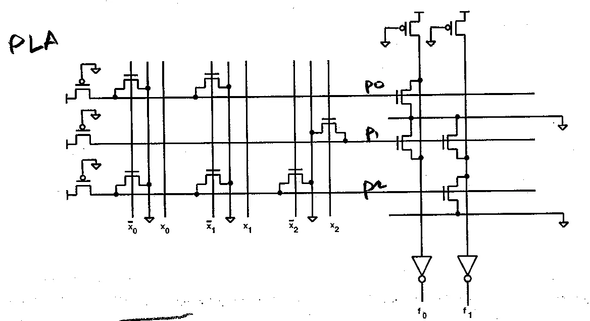
Reading the figure. Under the rows, the vertical lines repeat in threes, labelled at the bottom: , a ground line, . Each NFET’s gate is the short bar on a literal line; its two terminals join the row and the ground line next to it. At the right, each column’s NFETs are gated by the rows and join the column to the horizontal ground lines. Both columns end in inverters.
Part (a): f0 and f1 (9 points)
FN12-10a, p14. In the following circuit, find f0 and f1 (Boolean equations) as a function of x0, x1, and x2. (9 points)
Hint
What it asks. Two Boolean functions read off a transistor drawing: what and are for each input combination, as equations. The unknowns are the three product terms the rows make and which of them each output collects. The word that decides the method is “circuit”: the answer comes from the devices, so every device’s gate line and every inverter matters.
The idea. Each row is a pseudo-NMOS NOR of the lines its devices sit on, which is the AND of the complements of those lines: a product term. Each column is a NOR of the rows that have devices in it, and the inverter under it turns that into an OR. So the PLA is a sum of products: read the rows, read which rows each column uses, write the sums, and simplify.
Why this formula. Row ; output OR of its column’s rows (inverter present).
- Where it comes from. A pseudo-NMOS row is low if any of its NFETs is on, high otherwise (Chapter 18 §2): a NOR. De Morgan’s law turns the NOR of the lines into the AND of their complements (Chapter 18 §1). The column is the same gate turned on its side, and the inverter undoes its final NOT.
- Conditions. The pull-ups are weak enough that one on NFET wins (the pseudo-NMOS ratio, which the paper assumes); the inputs and their complements are both available on the lines. Both hold in the figure.
- The tempting alternative. Reading a device’s line as the literal itself: a device on means the row needs , not .
FN12-10a
- Row (the key’s p0). Because its devices’ gates are on and , it is high only when both lines are 0: .
- Row . Because its one device’s gate is on (its left terminal on the ground line between and , its right one on the row): .
- Row . Because it has devices on , and : .
- The columns. Because the left column has devices gated by and and an inverter after it, . The right column has devices gated by and : .
- Simplify . Because (if the first term is already 1; if the second term is ): . Row adds nothing that and do not already cover.
FN12-10a read (new figure): each row’s product at its right, each column’s sum below. The input traced: the lines at 1 (, , ) are thick, and every device they turn on (arrows) pulls its row low, so all three rows are 0 and , as gives for 101.
Check. By two input rows traced through the grid. : every complement line is 0, so and stay high; the line is 1, so is pulled low. Both columns see a high row, fall, and invert to 1: , and the formula gives . : the line is 1, which pulls down and , and pulls down . No row is high, both columns stay high, and the outputs are 0; the formula gives . The model evaluatePla runs all eight input rows: on 000, 010, 100, 110 and 111.
Answer: , , ; ; , the same function as .
Remember. A device on a line means the complement of that line’s literal is in the product. Read rows, then columns, then look for the inverters; finish by simplifying, because a PLA programmed by hand need not be minimal.
The answer key agrees
FN19-6: a dynamic PLA and its replica clocks (18 points)
You need
Precharge and evaluate (Chapter 18 §7). In a dynamic PLA each row’s pull-up is a PFET gated by , with an NFET foot gated by under its devices; each column’s by . Clock low: the PFET charges the node high, the foot is off. Clock high: the node falls if any of its devices is on, and otherwise floats high. Once evaluated, every row and column holds the NOR of its inputs, as in a static PLA.
The race and the two clocks (Chapter 18 §7). During precharge every row is high. If the OR plane evaluated while a row whose product is false was still falling, that row would discharge its column for good. So may rise only after the slowest row has evaluated, and ‘s low pulse must be long enough for the slowest row to precharge.
The question (FN19-6, p13, in the paper’s words). Consider the following dynamic PLA structure.
FN19-6’s dynamic PLA (Final 2019, p13, redrawn; dashed lines are virtual-ground lines). drives the rows’ PFETs and the AND plane’s foot (top left); drives the columns’ PFETs and the OR plane’s foot (right). The columns are the outputs , : there are no output inverters.
The exam’s own figure (FN19-6, p13)
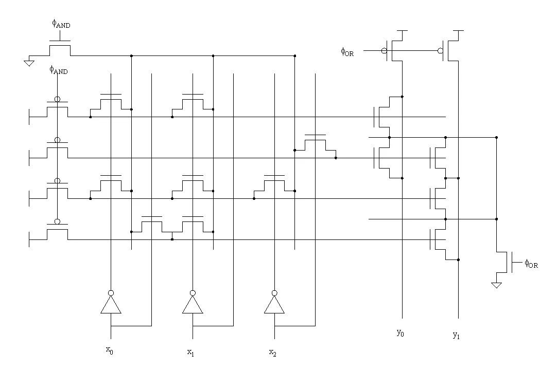
Reading the figure. The literal lines are made at the bottom: each input runs up as the true line, and an inverter beside it makes ; the vertical lines between them are virtual-ground lines, joined at the top and grounded through the foot. It is the lecture’s four-row example (Chapter 18 §3) made dynamic, and FN12-10a’s PLA with a fourth row.
Part (a): the logic function (10 points)
FN19-6a, p13. We discussed in class how it is necessary to derive the clocks and in such a manner that the OR plane does not being (sic) to evaluate until after the AND plane has evaluated. Furthermore, both and must allow for adequate precharge time. If the clocks satisfy this relationship, what is the logic function of this PLA (i. e, what are and as a function of , , and )? (10 points)
Hint
What it asks. The steady logic function of the PLA, after both planes have evaluated in the right order: and as equations in , , . The question’s long preamble is a condition, not a task: “if the clocks satisfy this relationship” means the race is avoided, so the dynamic PLA computes exactly what a static PLA with the same devices would. The words that decide the answer are in the figure: no inverters after the columns.
The idea. After evaluation every row is the NOR of its device lines, a product, and every column the NOR of its rows. Without output inverters the outputs are the complements of the sums of products. So read the four products as for FN12-10a, form each column’s NOR, and simplify with De Morgan.
Why this formula. for the rows in each column.
- Where it comes from. A dynamic node precharged high falls during evaluate if any of its devices is on, and stays high otherwise: once settled it is a NOR, like a pseudo-NMOS node (Chapter 18 §4, last line). With the clock order of the question, every row has its final value before the columns evaluate.
- Conditions. The clocks meet the two requirements (given); the inputs are stable during evaluate.
- The tempting alternative. Copying FN12-10a’s habit and writing : that ignores that this paper draws no inverters. The OR form would be the complement of the right answer on every row.
FN19-6a
- The rows. Because each row is the NOR of its device lines (call them to from the top): has devices on , : . has one on : . on , , : . on and : .
- . Because its column has devices gated by and and no inverter: .
- . Because its column has devices gated by , and : . The first term forces for to be 1; with the rest is . So .
- A cross-check with FN12-10a. Because ‘s column uses the same two rows as FN12-10a’s , but without the inverter, : the two papers’ PLAs give complementary first outputs.
Check. By the truth table, traced through the grid for two rows. : pull down , , and (via ); pulls down . No row high: both columns stay precharged, ; the formulas give and . : and stay high, so both columns fall: ; the formulas give and . The model evaluatePla over all eight rows: on 001, 011, 101 and on 001, 101.
Answer: ; .
Remember. A dynamic PLA, once its clocks are right, computes what the static one computes. Look for the output inverters before writing the answer: without them each output is the complement of its column’s sum of products.
The answer key agrees
Part (b): a replica AND row for both clocks (8 points)
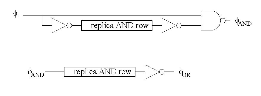
FN19-6b, p14. Design a replica AND row, two instance (sic) of which can be used in the circuits below to generate and to meet the timing constraints described in (a). (8 points)
FN19-6b’s clock generators (Final 2019, p14, redrawn; each box is the paper’s “replica AND row”). Upper: is the NAND of and the inverted output of a replica row clocked by . Lower: is the inverted output of a replica row clocked by .
The exam’s own figure (FN19-6b, p14)
Hint
What it asks. A transistor-level design of one dynamic row, a “replica”, to be dropped into both boxes of the paper’s figure, so that ‘s low pulse is long enough for the AND plane to precharge and rises only after the AND plane has evaluated. The decisive words are “a replica AND row, two instance of which”: one design, used twice.
The idea. A replica is a copy of the circuit whose delay must be waited for, built and placed the same way, so that it slows down and speeds up with the real rows at every corner of process, voltage and temperature (Chapter 18 §8). In the upper generator the replica’s precharge sets how long stays low; in the lower one its precharge sets when falls and its evaluate sets when rises. So the one row must precharge at least as slowly as the slowest real row and evaluate at least as slowly as the slowest real row.
Why this formula. The generators’ edges (Chapter 18 §9): and , where and are the replica’s.
- Where they come from. Upper: rises, the NAND falls (); falls one inverter later and the replica precharges; when it is high the second inverter drops the NAND’s other input and rises. Lower: rises, the replica evaluates, and when it has fallen the inverter raises .
- What makes a row slow. Precharge: the most capacitance on the row node, which is the most devices (the maximum literal count, 3 here: row ) with their internal node charged too. Evaluate: the fewest devices on, one, discharging the row alone (Chapter 18 §9).
- Conditions. The replica is laid out like a real row, sits in the same array, and drives the load of the most heavily loaded real row (the full row wire and as many OR-plane gates as any row drives), or its delays are not the worst real row’s.
- The tempting alternative. Two different rows, all devices on for and one on for , as the lecture builds them. That works, but the paper asks for one design used twice (Chapter 18 §9).
FN19-6b
- Start from a real row. Because the replica must track the real rows, copy one: a precharge PFET from to the row node and an NFET foot to ground, both gated by the replica’s clock input (the signal entering the box: in the upper generator, in the lower), laid out in the same array.
- Give it the maximum literal count. Because the slowest precharge belongs to the row with the most devices, give it three NFETs in parallel between the row node and the foot, as many as the widest product (, ). Their drains load the row node like the heaviest real row.
- Turn exactly one device on. Because the slowest evaluate is a row discharging through a single device: tie one NFET’s gate to and the other two to ground. In the lower generator the row then evaluates as slowly as any real row can, so rises only after every row has settled. In the upper generator it still precharges the node between the devices and the foot, through the one on device, so its precharge is at least as slow as the heaviest real row’s.
- Load it like the most heavily loaded real row. Because a row’s delay depends on what it drives, and the replica must be at least as slow as every real row: two OR-plane gates here ( feeds both and ; , and feed one each), on dummy columns, plus the full row wire, before the generator’s inverter. The replica then has the most drains (3) and the most gate load (2), so it is the slowest of the real rows on both counts.
- Place both instances. Because the two boxes need the same behaviour: the same design in both, as dummy rows inside the PLA’s array. The upper one makes ‘s low pulse , longer than any row’s precharge; the lower one makes fall a replica precharge and an inverter () after falls and rise after it rises, after the slowest row’s evaluate.
The FN19-6b answer (new figure): one replica AND row, used in both boxes. It copies a real row with the most devices (three), turns exactly one on (gates , 0, 0) so it discharges as slowly as the slowest real row, and carries , the heaviest real row’s wire and OR-plane gate load. Its clock input is in the upper generator and in the lower.
Check. By the two requirements with Chapter 18’s example delays (, , , ps, for example): is low from 30 to 220 ps, 190 ps, more than the 150 ps precharge (requirement 1, with to spare); rises at ps, after the slowest row finishes at 420 ps (requirement 2, with to spare). One condition is new with the single design: in the upper generator the replica must evaluate again, through its one device, while is low, so ‘s low phase must cover ps; at the example’s 640 ps period with a 50 % duty, the low phase is 320 ps.
Answer: One replica row, used in both boxes: a copy of a real AND row (precharge PFET and foot on the replica’s clock input), with the maximum literal count of NFETs, three, of which one has its gate tied to and two to ground, and its output loaded like the most heavily loaded real row’s (two OR-plane gates, as has, plus the full row wire). It evaluates through one device (the slowest evaluate, which times ) and precharges a full row with its internal node (at least the slowest precharge, which times ‘s low pulse).
Remember. A replica copies the worst real case for the edge it times: most capacitance for precharge, one device on for evaluate. One row with all devices present and one on serves both.
The answer key agrees
Harder variations: PLAs
You need
Reading and building a PLA (Chapter 18 §1–§5). Each row is a NOR of the literal lines its devices sit on, a product of the complements: a true literal in a product puts a device on the line. Each column is the NOR of its rows; with an inverter it is their OR. Fewer rows means a smaller PLA: Espresso finds a small shared cover, and rows can be shared between outputs when one product is an implicant of both.
The dynamic PLA’s clocks (Chapter 18 §9). With clk rising at 0: falls at and rises at ; falls after falls and rises after rises; the outputs are valid an OR-plane evaluate later, and the period must add the output latch’s setup.
These two variations added are harder than FN12-10a and FN19-6 in the ways the real midterm was: Variation 6 runs the other way, from a function to a programmed PLA, its minimum size, its device count and what the race does to it, a six-part chain; Variation 7 puts the replica clocks at a slow corner, against a fixed delay, with heavier arithmetic. Budgets assume about 1.8 minutes a point. No key exists.
Variation 6: a full adder as a PLA (about 25 minutes)
Variation 6: a full adder as a PLA
added The question. Build a full adder as a NOR–NOR PLA with output inverters: inputs , , ; outputs and . (a) Write each output as a sum of products. (b) What is the fewest rows the AND plane can have, if rows may be shared between the outputs? Justify. (c) Program the rows: on which literal lines do the devices go? (d) Count the devices of the static (pseudo-NMOS) version, output inverters included (not the input inverters that make , as in Chapter 18 §2). (e) The PLA is made dynamic, and by mistake both planes get the same clock. Which entries of the two truth tables come out wrong? (f) With two proper clocks, how many NFETs does the replica row need?
Hint
What it asks. The reverse of FN12-10a: from two functions to a programmed PLA, with a proof that it is as small as it can be, its cost in devices, and the failure the dynamic version suffers without its two clocks. What is unfamiliar is the minimality argument and the race count on a PLA no paper draws.
The idea. The carry is 1 when at least two inputs are 1; three products of two literals cover it. The sum is the parity of three bits: 1 on 001, 010, 100, 111. Any two of those differ in two bits, so no product of fewer than three literals fits inside the parity function: it needs four rows. Rows could be shared between the outputs only where a product is an implicant of both, and only 111 is; sharing it saves nothing, because the carry’s other three 1s still need three rows. So seven rows is the minimum.
Why this formula. Row devices: a true literal in the product puts a device on , a complemented on . Device count (static): one NFET per programmed crossing, one PFET load per row and per column, two devices per output inverter (Chapter 18 §2).
- Where it comes from. The row is the NOR of its device lines, which is the AND of their complements (Chapter 18 §1).
- The race with one clock. At the start of evaluate every row is still high from precharge, so every column with any device discharges, whatever the inputs; a column cannot rise again before the next precharge (Chapter 18 §7). With an output inverter every output then reads 1 in the worst case.
- Conditions. The worst case of the race: the columns discharge faster than the false rows fall.
Variation 6
- (a) Sums of products. Because the carry is the majority and the sum the parity: ; .
- (b) The fewest rows. Because the parity’s four 1s (100, 010, 001, 111) are pairwise two bits apart, each needs its own product: 4 rows. The carry’s 1s are 011, 101, 110, 111; its three two-literal products are prime and each is the only one covering one of 011, 101, 110, so they are all needed: 3 rows. Only 111 is an implicant of both outputs; letting the carry use the parity’s 111 row would still leave 011, 101 and 110, pairwise two bits apart, needing three more rows. So 7, and the exhaustive search of the model
minimumCoveragrees. - (c) Programming. Because a true literal puts its device on the complement line: on , ; on , ; on , ; on , , ; on , , ; on , , ; on , , . The column has devices on the first three rows, the column on the last four; each column ends in an inverter.
- (d) Devices. Because each programmed crossing is one NFET: AND plane , OR plane , loads PFETs, inverters : 38 devices.
- (e) One clock on both planes. Because every row is high when evaluation starts, both columns discharge on every input, and after the inverters both outputs read 1. They are wrong wherever the right value is 0: on 000, 001, 010, 100 and on 000, 011, 101, 110, 8 of the 16 entries. The 1s are right by luck.
- (f) The replica. Because the widest product has three literals, the replica row has three NFETs (one on, in FN19-6b’s single design).
Variation 6’s full adder in FN12-10a’s style (new figure; checked on all eight input rows): three rows for , four for , each true literal’s device on the complement line.
Check. By the model: plaFromTable builds the seven-row PLA, plaTables gives and on all eight rows, staticPlaDevices counts 18, 7, 9 and 38, and sharedClockColumns gives 1 on both outputs for every input. By one row traced by hand: has , so the row (devices on , ) stays high and the column falls: . For : but , so the rows (device on ), (on ) and (on , ) are pulled low, and is pulled low by : , and .
Answer: (a) , . (b) 7 rows: the parity’s four minterms are isolated, the carry’s three primes are all essential, and the one shareable product, , saves no row. (c) As in step 3. (d) 38 devices. (e) Every output reads 1: wrong on the 8 entries where the right value is 0. (f) Three NFETs.
Remember. Parity is a PLA’s worst case: no two of its 1s are adjacent, so every minterm costs a row. To prove a cover minimal, show that each product is forced, not that you could not find a smaller one.
Variation 7: the replica clocks at a slow corner (about 25 minutes)
Variation 7: the replica clocks at a slow corner
added The question. FN19-6’s PLA is clocked by FN19-6b’s generators with the single replica row. At the typical corner, , , the replica’s precharge and evaluate , the OR plane’s evaluate 150 and the output latch’s setup 50 ps (for example). (a) Find the four clock edges, the outputs’ valid time and the shortest period at the typical corner. (b) At a slow corner the gates (inverters, NAND, latch) are 10 % slower and every row and column 30 % slower. Recompute (a). (c) Do the two requirements still hold, and with what margins? (d) A designer replaced the lower replica by a fixed inverter chain tuned to the typical ; it slows like the gates. What happens at the slow corner? (e) What must clk’s high and low phases cover at the slow corner, and by how much must the period grow?
Hint
What it asks. The generators’ timing worked twice, then the point of a replica made quantitative: at a corner where rows slow more than gates, the replica keeps both requirements and a fixed delay does not. Heavy arithmetic, one chain.
The idea. Each edge is a sum of gate delays and replica delays. The replica’s terms scale with the real rows, so the requirement margins, which are made of gate delays only, stay positive at every corner. A fixed chain’s delay scales with the gates, so when the rows slow more, the OR plane starts before the slowest row has finished.
Why this formula. With clk rising at 0 (Chapter 18 §9): ; ; ; ; valid ; period valid + setup.
- Where it comes from. Tracing each generator edge by edge (FN19-6b’s steps).
- The margins. Requirement 1: . Requirement 2: . Both are gate delays only, positive at every corner.
- Conditions. The replica’s and are the slowest real row’s at every corner (it is a real row); the delays are rounded to whole ps.
Variation 7
- (a) Typical. ; (low 190); ; (low 240); valid at ; period ps.
- (b) The slow corner’s delays. Because gates are 10 % slower and rows 30 %: , , setup 55; , , the OR plane 195 ps.
- (b) The slow corner’s edges. ; (low 239); ; (low 304); valid at ; period ps.
- (c) The requirements. Because the margins are gate delays: requirement 1, ps (); requirement 2, the slowest row finishes at and rises at 554, 22 ps later (). Both hold.
- (d) A fixed chain. Because it was tuned to ps and slows like a gate, it gives 242 ps at the slow corner, while the slowest row needs 260: rises 18 ps before the slowest row has evaluated. For those 18 ps a falling row is still high while the OR plane evaluates, and its column can discharge for good: a wrong 0 on or (no inverters), the race of Chapter 18 §7.
- (e) clk’s phases. Because clk’s high phase must outlast ‘s low pulse (239 ps), and its low phase must let the upper replica evaluate again through its one device, ps: at the 804 ps period with a 50 % duty both phases are 402 ps, enough. The period grows from 640 to 804 ps, 25.6 %, so the clock must slow down at that corner; the replicas stretch the clocks but cannot shorten the logic.
Variation 7’s clocks (computed with the example delays): (a) typical, (b) the slow corner with gates 10 % and rows 30 % slower; times in ps, the minimum period. Dashed: from a fixed delay tuned at nominal, which rises at ps, 18 ps before the slowest row finishes at ; the replica’s rises at 554.
Check. By the closed form for ‘s low time, : typical , slow , as in steps 1 and 3. The model plaClockEdges gives the same eight numbers at each corner. Scaling sense: every term grew by 10 % or 30 %, so the period’s growth, 25.6 %, must lie between them, and it does, nearer 30 % because the rows dominate the path.
Answer: (a) low 30–220 ps, low 200–440 ps, valid 590 ps, period ps. (b) low 33–272 ps (239), low 250–554 ps (304), valid 749 ps, period ps. (c) Yes: margins 44 ps () and 22 ps (). (d) The fixed chain gives 242 ps against the 260 ps the slowest row needs: requirement 2 fails by 18 ps, and a column can discharge to a wrong 0. (e) High phase ps, low phase ps; the period grows 25.6 %, to 804 ps.
Remember. A replica’s margins are made of gate delays, so they survive every corner; a fixed delay’s margin is a difference between a gate chain and a row, and it changes sign when the rows slow more than the gates.