F2. Past finals: inverters, chains and low-voltage operation
The past finals ask the midterm’s inverter questions again, with one new twist: the inverter run below threshold. This page re-solves every final-exam part on inverters and inverter chains that uses midterm material: an inverter at 0.2 V (its off-current, its , its delay and its power), and chains of inverting stages (their delay, their energy per transition and the width that minimizes the delay).
| Exam | Parts on this page | Answer source |
|---|---|---|
| Fall 2019 (FN19) | 1a–d, 3a–d | an unfilled exam: no key |
| Fall 2017 (FN17) | 10a–b | the revised key |
| Fall 2010 (FN10) | 2a–b, 4a–b | the key |
Every number below is re-solved here; none is copied from a key. FN19 has no key, so its solutions are this guide’s own. Where a key disagrees, the folded note on the key at the end of the part explains why, and the table at the end lists them.
Left out. FN17-10c (the supply that minimizes the chain’s energy) and FN10-2c (the lowest supply that still gives a 10–90% swing) need low-voltage and minimum-energy operation, which the course does not teach before the midterm. The other questions on these exams (latches and clocking, wires, power grids, test, memory, datapath blocks, PLAs) are later material. The device questions of the same finals are on F1, path sizing on F3, and pass-transistor and dynamic logic on F4.
After this page you can:
- find an off-current from a current at threshold and the subthreshold slope, and an ratio above and below threshold;
- estimate a low-voltage inverter’s delay with the constant-current 50% formula, and its average power from switching and leakage;
- write a subthreshold chain’s delay as a function of ;
- turn a gate with stacked devices into a gain, and get a chain’s delay and energy per transition with a symbolic side load;
- say why “the width that minimizes delay” has no finite answer when the load is fixed, and what happens when there is no fixed load.
Before you start
How to use this page. Each section restates one exam question with its source page (FN19-1c, p3 is Fall 2019, question 1c, physical PDF page 3) and its points, and shows the exam’s own figure. The inverter below threshold is new on the finals, so it opens with a How to approach section: how to recognize the question, the moves in order, why the formulas apply, and the traps. The chains are the midterm’s inverter-chain family, which M3’s approach section teaches; their parts say what is new. Every part is worked the same way: what it asks, the idea behind the method, the solution in steps (each step gives its reason first), a check on the result, the answer, and one thing to remember. Try each part on your own first; open the Hint if you are stuck, and step through the solution before you press “Show all”. Where there is a key, its verdict is folded at the end of the part. The chapters teach each method in full, and every solution links the section.
| Family | Questions (newest first) | Chapters | Midterm twin |
|---|---|---|---|
| An inverter below threshold | FN19-1, FN17-10, FN10-2 | 4, 5, 6 | the off-current of MT23-1b and MT24-2b (M3) |
| Chains: delay, energy, best width | FN19-3, FN10-4 | 6, 7 | MT24-2, MT21-4, MT17-4 (M3) |
Conventions the exams use
State these at the top of your answer.
- Currents per device. FN19-1, FN17-10 and FN10-2 give currents per transistor, not per µm, and the same numbers for the NFET and the PFET, so rise and fall are alike.
- Subthreshold current falls tenfold for every volts of gate voltage below threshold (Chapter 4, Section 11). The finals say “ignore DIBL”, so it does not depend on .
- Delay at constant current. With a constant current , the output reaches 50% after added (Chapter 6, Section 10), Chapter 5’s (Section 11) taken to the 50% point. The full swing takes twice as long.
- Delay in τ. FN19-3 and FN10-4 give the fan-out-of-one delay and in fF/µm. Both size the PFETs 2W against W NFETs, so , the inverter’s input is and (Chapter 7, Section 7). A stage’s delay is its gain times ; no 0.69 factor; drain capacitance is ignored.
- Energy per transition. One input edge through a chain: half the nodes rise and half fall. The rising nodes draw each from the supply; counted as dissipation instead, every switching node burns . Both counts give the same total (Chapter 6, “Energy in a chain of gates”). A square wave’s cycle charges every node once.
How to approach a subthreshold-inverter question
Recognize it by a supply below the threshold (“let V”, “this will be subthreshold operation”), by the words “”, “subthreshold slope” and “ignore DIBL”, and by a single inverter or a chain of identical ones with a load in fF. The parts come in the same order on every final: the off-current, the on/off ratio, the delay into a load, and sometimes the power or the chain’s delay as a function of . The family carried 40 points of FN19 (FN19-1), about 16 of FN17 (FN17-10a–b) and 15 of FN10 (FN10-2a–b).
The moves, in order.
- Compare with . It decides which current law the “on” device obeys: above threshold the question’s law, below it the subthreshold line. The “off” device () is always on the subthreshold line.
- The off-current from the calibration point, in decades. If the question gives the current at , count the decades of from down to and divide the current by ten for each. If it gives itself (the current at ), you already have it.
- The on-current. Above threshold, from the question’s law; below it, from the same subthreshold line at . Below threshold the ratio is simply .
- The delay at constant current. The switching device carries into the load until the output crosses 50%: . A chain of identical stages takes times that.
- The power. Switching, at the switching frequency , plus leakage, . First check that the output finishes its swing within half a period, because the switching count assumes it does.
Why these formulas.
- The subthreshold line. Below threshold the current is set by carriers crossing a barrier with their thermal energy, so it falls exponentially as the gate drops: one decade for every millivolts below : for (Chapter 4, Section 11). With DIBL ignored the drain voltage doesn’t enter, so lowering doesn’t change . Divide the on state by the off state and and cancel: .
- The above-threshold law. FN19-1 gives , the fully velocity-saturated current of Chapter 4, Section 7. It holds only above and with the drain saturated.
- Delay as charge over current. A node of capacitance holds ; a constant current moves half of it, enough to cross the 50% point that defines delay, in added (Chapter 6, Section 10). Below threshold the current depends only on , which stays at once the input has switched, so a constant current is a fair estimate.
- Power. Each rise of the output draws from the supply (Chapter 6, Section 6), once per period, so the switching power is that energy times the frequency . The off device leaks with across it all the time, so the leakage power is (Chapter 4, Section 11; M3’s MT24-2b).
Decisions to make on the way. Per device or per µm (these finals give currents per device). The delay to 50% or the full swing (the course measures 50% to 50%; say which you use). Which load each stage drives (in FN17-10 the end load is one more inverter).
Traps. The above-threshold law below threshold: it gives a negative current. The factor of 2 between the 50% delay and the full swing (FN17-10b’s key). Expecting the two current laws to meet at : they are separate fits added. A lower changing (not with DIBL ignored). Counting the switching energy when the output can’t finish its swing.
1. FN19-1: a low-voltage inverter
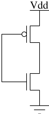
FN19-1, p2 (Fall 2019, 40 points). An inverter with supply ; logic swings between ground and . V for the NFET and V for the PFET. Above threshold, with mA/V for the NFET, and with 1 mA/V for the PFET. is the current at () with (); is the current at () with .
The two devices are mirror images: the same , the same 1 mA/V, and (in part a) the same subthreshold calibration. Every answer holds for both.
FN19-1a: off-current and the on/off ratio at 1.2 V
FN19-1a, p2 (10 points). Let V. If the current of the NFET (PFET) is 100 µA at () of and () of 0.32 V, what is the off-current? Assume a subthreshold slope of 90 mV/decade and ignore DIBL. What is the ratio for each transistor?
Hint
What it asks. Two currents of one transistor and their ratio. The off-current is the leak of a transistor whose gate is at 0 V; the on-current is the current with the gate at the full 1.2 V. The phrase “at of 0.32 V” decides the method: the 100 µA is a calibration point on the subthreshold line, exactly at threshold.
The idea. The course uses one current law per region, so first place each state against (the approach). Off, is below threshold: the current lies on the subthreshold line, falling one decade for every millivolts below (Chapter 4, Section 11):
On, V is well above threshold, and the question’s law applies: , the fully velocity-saturated current of Chapter 4, Section 7, valid with the drain saturated (). The off-current is the move of MT23-1b and MT24-2b (M3), for a whole device instead of a µm. added The two current models don’t meet at threshold: the above-threshold law gives 0 at , the subthreshold calibration 100 µA. Each is a fit for its own region; use the one the question puts you in.
FN19-1a
- Place each state. Because the law depends on the region: off, V, subthreshold; on, V, above threshold.
- Count the decades to the off state. Because the line falls one decade per 90 mV below , count from the calibration point down to , 320 mV at 90 mV per decade: decades, a factor of .
- The off-current. Because the current falls by that factor, divide the current at threshold by it: . The PFET is the mirror image, with , so it leaks the same.
- The on-current. Because the on state is above threshold with , the question’s law holds: .
- The ratio. With both currents known, divide: .
Check. Count the ratio in decades instead. From the off state up to threshold is 3.56 decades; from threshold to the on state the current grows from 100 µA to 0.88 mA, a factor of 8.8, or decades. Together decades, and . ✓
Answer: nA and , for each transistor.
Remember. An off-current is the current at threshold divided by : count the decades from down to 0. Place each state against before choosing a law.
FN19-1b: the on/off ratio at 0.2 V
FN19-1b, p3 (10 points). Now let V. What is the ratio for each transistor?
Hint
What it asks. The same ratio with the supply lowered to 0.2 V. The “on” device now has V, and the “off” device still has , with only 0.2 V across it. The number that decides the method is 0.2 V: it is below the 0.32 V threshold.
The idea. Move 1 of the approach: compare with . Here both states lie on the subthreshold line, so the ratio is just the decades between and . Write both currents with the line of (a) and divide: and cancel, and . The tempting wrong method is the question’s above-threshold law: mA, a negative current, which says the law doesn’t apply below .
FN19-1b
- Place the on state. Because V, even the “on” device is below threshold: it is on the subthreshold line, not on the above-threshold law.
- The on-current. Because the on device is on the subthreshold line, count its decades below : 0.2 V is mV below, that is decades: .
- The off-current. Because is set at , and with DIBL ignored the lower drain voltage doesn’t change it, it stays 27.8 nA from (a).
- The ratio. With both currents on the same line, divide: .
Check. The shortcut gives it without or the 100 µA: . ✓
Answer: for each transistor, against at 1.2 V: below threshold the supply buys only one decade of on/off ratio per 90 mV.
Remember. Below threshold , whatever the threshold and the calibration: one decade per of supply.
FN19-1c: delay at 0.2 V
FN19-1c, p3 (10 points). If this inverter drives a load of 10 fF, estimate the delay of this inverter at V.
Hint
What it asks. How long the inverter takes, at 0.2 V, to switch a 10 fF load: the delay from the input’s 50% point to the output’s. “Estimate” invites the simplest model: a constant current.
The idea. Delay is charge over current: Chapter 5’s (Section 11). The course measures delay between the 50% points (Chapter 6, Section 10), so the switching device has to move only half the charge , and with a constant current that takes added. A constant current is a fair estimate here: below threshold the course’s current depends only on (DIBL is ignored), and stays at once the input has switched. The tempting slip is , the time for the full swing: twice the delay.
FN19-1c
- The current that switches the load. Because the input switches fully, to 0.2 V or to 0, the switching device has V and carries from (b).
- The current against it. Because the other device is off, it leaks 27.8 nA the other way: 0.6% of , negligible.
- The charge to move. Because the delay ends at the 50% point, the device must move half of : .
- Both edges. Because the two devices are mirror images with the same current, the rising and falling outputs take the same time.
Check. Units: a femtocoulomb at a microampere takes a nanosecond, so ns. ✓ And the size is plausible: the same estimate at 1.2 V (in the answer) is about 30 times faster, because the current there is about 190 times larger while the charge is only 6 times larger.
Answer: about 215 ps to the 50% point. The full swing, , takes 431 ps. For comparison, at 1.2 V the same estimate gives ps: dropping the supply below threshold costs a factor of about 30 in speed.
Remember. At constant current the delay to 50% is ; the full swing takes twice as long. Below threshold is tiny, so the delay is long.
FN19-1d: average power at 1 GHz
FN19-1d, p4 (10 points). If the inverter (with V) is stimulated with a 50%-duty-cycle square wave at its input switching between 0 and 0.2 V with a period of 1 ns, what is the average power consumed by this inverter?
Hint
What it asks. The inverter’s average power when a 1 ns square wave drives it at 0.2 V: the energy it uses in one period, divided by the period. “50% duty cycle” means each output swing has half the period, 500 ps.
The idea. A static inverter spends power in three ways. Switching: each rise of the output draws from the supply (Chapter 6, Section 6), once per period, so . Crowbar: current straight through both devices while a slow input edge holds both on (Chapter 6, Section 7). Leakage: the off device, with across it, leaks all the time, . Below threshold one new question comes first: the count assumes the output reaches the rail, and at these currents the swing is slow. Keep the 10 fF load of (c): the question names “the inverter” of the previous part.
FN19-1d
- Does the swing finish? Because the switching count assumes a full swing, compare its time with the 500 ps available: the full swing takes ps (c), so it just finishes. Assume a full swing.
- Switching. Because the output rises once per period, it draws per period. At GHz: .
- Crowbar. Because a square wave has instant edges, the two devices are never on together: none.
- Leakage. Because in either state one device is off with across it: .
- Add them. Because the three parts draw energy independently, the average power is their sum: ; leakage is 1.4% of it.
Check. Count energy per period instead: 0.4 fJ of switching, plus fJ of leakage. A femtojoule per nanosecond is a microwatt, so the average is . ✓
Answer: about 0.41 µW (0.400 µW switching plus 5.6 nW leakage). The full-swing assumption is tight: with a period shorter than about 0.86 ns (twice the 431 ps swing) the output would no longer reach the rails in this estimate, and the switching energy per cycle would shrink.
Remember. Average power = + (+ crowbar for slow edges). Below threshold, first check that the output finishes its swing in half a period.
Check yourself For FN19-1’s devices, at what supply below threshold is Ion/Ioff = 1000, and what is the 10 fF delay there?
Three decades at 90 mV/decade: V, still below V. Then , and ps. Another 70 mV of supply makes the inverter 4.4 times faster than at 0.2 V.
2. FN17-10: a subthreshold inverter chain
FN17-10, p21 (Fall 2017; the point values are overwritten and appear to be 8 per part). A chain of eight identical 10 µm/5 µm inverters, loaded at the end by 30 fF. “We are going to calculate the supply voltage at which this inverter chain will consume minimum energy. This will be subthreshold operation.” The gate capacitance is 2 fF/µm.
There is no figure. Each inverter’s input is , so the 30 fF at the end is one more inverter: every stage drives 30 fF, and the eight stages are identical. Part (c), the supply for minimum energy, is left out (see the top of the page).
FN17-10a: the on-current against the supply
FN17-10a, p21. Assume the of each transistor is 10 nA. If the subthreshold slope is 80 mV/decade, what is the on-current of the devices of the inverter as a function of ?
Hint
What it asks. The on-current as a formula in , given the off-current (10 nA) and the slope (80 mV/decade). “This will be subthreshold operation” decides the law: the supply stays below threshold, so the on device is on the subthreshold line too.
The idea. The same subthreshold line as FN19-1, but calibrated at instead of at . Raising the gate from 0 to climbs decades, so (Chapter 4, Section 11). It needs no threshold, which is as well: the exam gives none. It holds only while stays below .
FN17-10a
- The calibration point. Because is defined at , it is the foot of the line: 10 nA at 0 V.
- The climb. Because the on device has , and the line rises one decade for every 80 mV, the current grows by .
- The formula. Because the line starts at and gains decades, multiply: , for both devices, which have the same numbers.
Check. At the formula gives back nA, as it must. ✓ At 0.2 V it climbs decades to 3.16 µA, the same as FN10-2a, which shares the calibration and the slope.
Answer: ; for example 3.16 µA at 0.2 V.
Remember. Below threshold, : a current calibrated at needs no .
The answer key agrees
FN17-10b: the chain’s delay against the supply
FN17-10b, p21. Estimate the delay of the inverter chain (as a function of ).
Hint
What it asks. The delay of all eight stages, as a formula in . Both the charge to move () and the current ( of (a)) depend on the supply, so both stay in the formula.
The idea. Each stage is FN19-1c’s constant-current estimate: it moves half the charge on its 30 fF load at the current , so to the 50% point added (FN19-1c; Chapter 6, Section 10). The stages are identical and switch one after another, so the chain takes eight times as long. The full swing, , would be twice as long; the course measures delay to 50%, and on an exam you say which you use.
FN17-10b
- The load and the current per stage. Because every stage drives one 30 fF input (above) and both devices carry from (a), every stage, rising or falling, sees the same 30 fF and the same current.
- One stage, to 50%. Because the delay ends when half the charge has moved: .
- Eight stages. Because the stages are identical and in series, their delays add: .
- Simplify. To read the formula, collect the constants: , so .
- Some values. To see the scale, put in three supplies: 67.5 ns at 0.1 V, 7.59 ns at 0.2 V, 640 ps at 0.3 V.
Check. The formula’s two parts should show up in the values. From 0.2 to 0.3 V the current grows by and the charge by , so the delay should fall by ; and . ✓ Each 80 mV of supply makes the chain almost ten times faster, a little less because the charge grows too.
Answer: , about 7.6 ns at 0.2 V.
Remember. A subthreshold chain’s delay goes as : about one decade of speed per of supply.
The answer key differs
It takes each inverter as , so the chain takes : twice the answer above. That is the time for a full swing at constant current, not the delay to the 50% point. Both are estimates, but the course measures delay from 50% to 50% (Chapter 6, Section 10), and the 2010 key uses , “delay to 50% point”, in the same problem (FN10-2b). On an exam, say which you use.
3. FN10-2: an inverter at 0.2 V
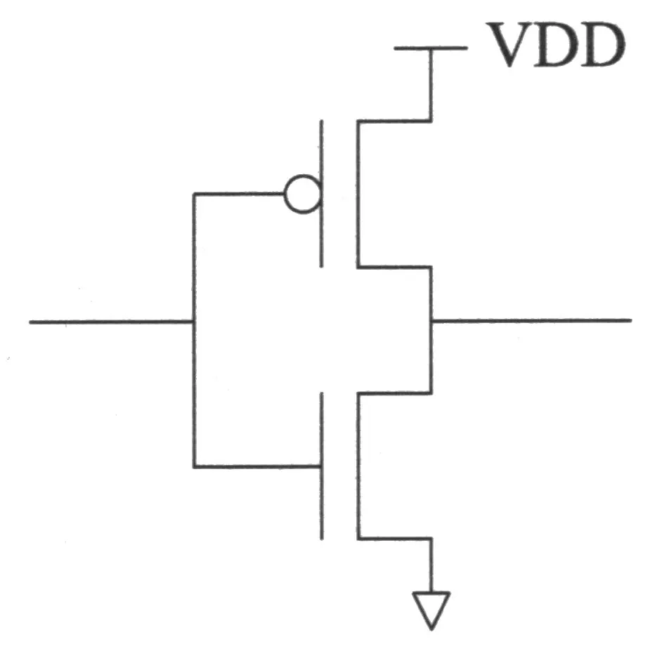
FN10-2, p3 (Fall 2010). An inverter with supply ; logic swings between ground and . The key adds by hand: “(assume V)”. and are defined as in FN19-1.
FN10-2a: the on/off ratio
FN10-2a, p3 (10 points). Let V. Assume that the of each transistor is 10 nA. If the subthreshold slope is 80 mV/decade, what is the ratio for each transistor?
Hint
What it asks. The on/off ratio at 0.2 V, given the off-current and the slope. The key’s handwritten “ V” decides the method: both states are below threshold.
The idea. This is FN19-1b’s shortcut. Both currents lie on the subthreshold line, one decade per , so their ratio is , and neither nor the calibration current enters (the approach). The differences from FN19-1 are a smaller slope, 80 mV/decade, and a calibration at , as in FN17-10a; the shortcut needs neither the threshold nor the 10 nA.
FN10-2a
- Place the on state. Because V, the on device, at V, is below threshold too: both states are on the subthreshold line.
- Count the decades. Because the line climbs one decade per 80 mV, between and V it climbs decades.
- The ratio. Because each decade is a factor of ten, , for both devices, and so .
Check. Compare with FN19-1b, at the same 0.2 V supply. A smaller slope packs more decades into the same voltage: 80 mV/decade gives decades where 90 mV/decade gave 2.22. So the ratio must be larger than FN19-1b’s 167, and 316 is. ✓
Answer: 316 for each transistor ().
Remember. Below threshold the on/off ratio depends only on : divide the supply by the slope and raise ten to it.
The answer key agrees
FN10-2b: delay at 0.2 V
FN10-2b, p3 (5 points). If this inverter drives a load of 10 fF, estimate the delay of this inverter at V.
Hint
What it asks. The delay of this inverter into 10 fF at 0.2 V: the same question as FN19-1c, with the devices of (a).
The idea. FN19-1c’s constant-current estimate: the switching device carries and must move half of to cross the 50% point, so added (Chapter 6, Section 10). Only the current differs from FN19-1c: (a) gives 3.16 µA where FN19-1 had 4.64 µA.
FN10-2b
- The current. Because the switching device has , it carries from (a); the off device’s 10 nA against it is 0.3% of that, negligible.
- The delay to 50%. Because the delay ends when half the charge has moved: .
Check. Same load, same supply as FN19-1c, so the delays should be in the inverse ratio of the currents: , and ps. ✓
Answer: about 316 ps to the 50% point. FN19-1c is the same question with 90 mV/decade and a different calibration: 215 ps.
Remember. At a fixed load and supply, the delay is inversely proportional to the on-current: find , and the rest is .
The answer key agrees
It writes “delay to 50% point” beside the formula .
Try it
Pick an exam’s device and move the supply. The solid curve is the delay to 50% (for FN17-10, the whole eight-stage chain); the dashed curve is one full swing; for FN19-1 the dotted line is the half period of the 1 GHz square wave of part (d). The supply slider stops at the threshold: 0.32 V for FN19-1, the key’s “ V” for FN10-2, and an assumed 0.3 V for FN17-10, which gives no threshold.
What to notice.
- The delay curve is almost a straight line on the log scale: one decade per 80 or 90 mV of supply, the subthreshold slope read sideways.
- FN19-1 at 0.2 V: the full-swing curve sits just below the half-period line, so the output finishes its swing in time (part d). Lower the supply below about 0.19 V and it no longer does.
- depends only on : compare FN10-2 and FN17-10, which share the slope but not the load.
4. FN19-3: a four-bit ripple-carry chain
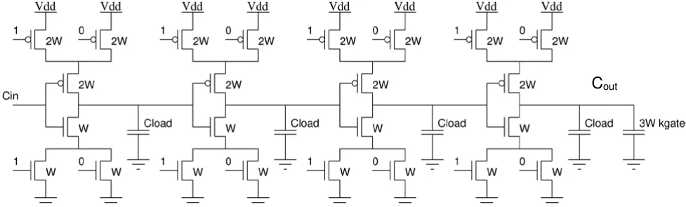
FN19-3, p7 (Fall 2019, 39 points). The carry chain of a four-bit static ripple-carry adder. models the loading of the sum circuit at each bit. Transistors provide fF/µm of loading. The fan-out-of-one (FO1) delay is ps.
Reading the circuit. Every part needs to know what one stage is, so read it once, device by device.
Reading FN19-3 device by device
- The fixed inputs. In every bit the other two gates are tied to 1 and 0, so the bit propagates its carry. A PFET conducts when its gate is low, so in the pull-up the PFET with gate 0 is on and the one with gate 1 is off. An NFET conducts when its gate is high, so in the pull-down the NFET with gate 1 is on and the one with gate 0 is off.
- What is left on each side. With the off devices gone, each side is the carry input’s device in series with one on device. Pull-up: the on 2W PFET in series with the carry input’s 2W PFET. Pull-down: the carry input’s W NFET in series with the on W NFET. So each stage is an inverter of its carry input with two devices in series on each side.
- The polarity. Because each stage inverts, the carry alternates polarity along the chain, and four inversions bring back to ‘s polarity.
- The node inside each stack. The node between a stack’s two devices is tied to its rail through the on device, so it stays there and does not switch: it adds no delay and no switching energy.
- The load on each output. Each output drives the next stage’s carry pin, one 2W PFET and one W NFET, , plus the sum circuit’s . The last output’s stands for the next bit, so all four nodes are alike.
Conventions. The 2W/W sizing says (the exam doesn’t state it). Then , so . Drain capacitance is ignored. has no value in the exam, so the answers keep it.
FN19-3a: delay with W = 1 µm
FN19-3a, p7 (10 points). If , what is the delay of the carry chain from to ?
Hint
What it asks. The time for a carry to ripple from to through four stages, with m. has no value, so the answer is a formula in it.
The idea. This is the midterm’s inverter chain; M3’s inverter-chain section teaches its moves: find the node’s capacitance first, read the strengths, then one stage is and the chain is stages. The new point is the stack. Devices in series act like one device of width , so two equal ones act like one of half the width (Chapter 7, “Two devices in series”). A carry stage therefore drives like an inverter half as strong as its input suggests: its logical effort is , and each stage costs even with no sum load. In gain form a stage takes , with its load over its input (Chapter 7, Section 9). The convention decides : with , .
FN19-3a
- The stack rule. Because two equal devices in series act like one of half the width, two W NFETs are one NFET of width W/2, resistance . Two 2W PFETs are one PFET of width W: . Both edges see the same .
- A stage’s input. Because the carry pin drives one 2W PFET and one W NFET, it presents , the same as a 2W/W inverter’s.
- The node. Because each output drives the next carry pin and the sum circuit (the reading block): .
- One stage. Because a stage’s delay is its resistance times its node’s capacitance, with written through : .
- The same as a gain. Because an inverter as strong as this stage (a W/2 NFET, a W PFET) has input , , and . The same .
- Four stages. Because the four identical stages switch one after another, their delays add: . With , fF: .
Check. The limiting case : each stage drives one copy of itself and takes ps, where a chain of plain inverters would take per stage, 100 ps for four. The series pairs double it, as step 1 said. And the slope’s units: , and kΩ × fF = ps. ✓
Answer: ; for example 400 ps if fF. The trap is to treat each stage as a plain inverter: the series pair doubles the resistance, so each stage costs even with no sum load.
Remember. A stack of two equal devices drives like one of half the width. A stage with a series pair on each side is an inverter with : per stage.
FN19-3b: energy of one propagated transition
FN19-3b, p7 (10 points). If V and , what is the energy dissipated by a single propagated transition through the carry chain?
Hint
What it asks. The energy of one carry edge rippling through all four stages, at 1.2 V and m. “A single propagated transition” decides the count: one edge, not a full cycle.
The idea. M3’s energy move (MT24-2a): a rising node draws from the supply, half stored and half burnt in the pull-up, and a falling node burns its stored half in the pull-down (Chapter 6, Section 6). So count the rising nodes and charge each . Per transition, half the nodes rise. What is new here: only the four outputs switch. The stack nodes stay at their rails (the reading block), and is charged by whatever drives the chain.
FN19-3b
- One node. Because at m the next carry pin is fF: .
- Which nodes switch. Because the carry propagates and each stage inverts, all four outputs switch, alternately: two rise and two fall.
- Price them. Because a rising node draws from the supply and a falling one draws nothing, the energy drawn is that of the two rising nodes, . Dissipated: each switching node burns , so . The same (Chapter 6, “Energy in a chain of gates”).
- The numbers. Because the question fixes V, : .
Check. Units: fF × V² = fJ. ✓ And the trap: per cycle (an edge and its return) every output would rise once, , twice as much. The question says a single transition.
Answer: (fJ, with in fF). Not counted: the node, charged by whatever drives the chain (as FN10-4b says outright), and the stack nodes, which stay at their rails.
Remember. Per transition, half the switching nodes rise: . A node held at a rail by an on device doesn’t count.
FN19-3c: the width that minimizes the delay
FN19-3c, p8 (9 points). What value of W will minimize the delay of this carry chain? What energy will be dissipated at this value of W for a single transition through the chain?
Hint
What it asks. The width that makes the chain fastest, and the energy per transition at that width. As in MT24-2e, the points are for saying what kind of answer there is, and why.
The idea. The same argument as MT24-2e; what differs is that each stage costs and the side load is a symbol. Split one stage of (a): . The first part is the stage driving the next stage: a wider stage is stronger by , but its load is larger by too, so this part is fixed. The second part is a fixed load driven by an ever stronger device: it shrinks as and never turns around. Setting a derivative to zero finds nothing.
FN19-3c
- Split the chain’s delay. To see which part depends on , write (a) as two terms: .
- Which part depends on W. Because only the term does, and it shrinks as grows, the delay falls every time grows: there is no finite minimum.
- The floor. Because as the sum load becomes negligible next to the gates, each stage drives only a copy of itself (), and ps. It approaches this floor but never reaches it.
- The energy. Because the gate part of every node grows with , the energy of (b), for any , is fJ. It grows in proportion to , without bound.
- The returns diminish fast. To see what a wider buys, compare the delay with the energy at two widths. With , the gates’ own load: at the delay is ps; at it is 222 ps, for five times the energy. So “minimize the delay” alone is not a design goal here. added Energy × delay, , is least where its growing part balances its shrinking part , at , as in MT24-2d and MT17-4d.
Check. The other end: as the delay grows without bound, because ever weaker devices drive a fixed . From there the delay only falls toward its 200 ps floor, so there is nothing in between to minimize.
Answer: no finite W: the delay keeps falling toward ps as , while the energy per transition, , grows without limit. This is MT24-2e’s “think carefully” answer (M3). added Outside the exam’s model, the stage driving would slow down as grows; the question leaves it out.
Remember. With a fixed side load and nothing else fixed, minimizing the delay has no finite answer: say so, give the floor (), and name the cost, the energy, that grows without limit.
FN19-3d: no sum load
FN19-3d, p8 (10 points). Repeat the calculation of (c) if .
Hint
What it asks. The delay-minimizing width and its energy again, now with no sum circuit on the outputs.
The idea. This is MT17-4a’s “does it depend on W?”. With no fixed load, each stage drives only a copy of the next stage. A wider stage is stronger by and its load is larger by , and the two cancel, so the delay is the same for every width (Chapter 7, Section 7). The energy still grows with , so the energy decides the width.
FN19-3d
- One stage. Because with each node is only the next stage’s : , for any .
- The chain. Because the four stages are alike and add, four such stages: ps, whatever .
- The energy. Because each node is now gate capacitance only, (b)‘s count gives fJ ( in µm).
- Choose W. Because every width gives the same delay and the energy grows with , take the smallest width the technology allows. At , 8.64 fJ.
Check. This is (c)‘s floor, reached: with no fixed load at every width, so the 200 ps that (c) approached as holds for every . And (b) with gives the same 8.64 fJ at 1 µm. ✓
Answer: the delay is 200 ps for every W, so W does not matter for speed; choose the minimum W, where the energy fJ is least (8.64 fJ at 1 µm). This is MT17-4a’s “does it depend on W?” (M3).
Remember. A chain that drives only copies of itself has the same delay at every size; then the smallest size wins, on energy.
Check yourself In FN19-3, let Cload = 3 fF. Which W minimizes energy × delay, and what are the delay and the energy per transition there?
Energy × delay , least where the gates’ load equals the side load: fF, so . The delay is ps, twice the floor, and the energy fJ.
5. FN10-4: four inverters with a side load
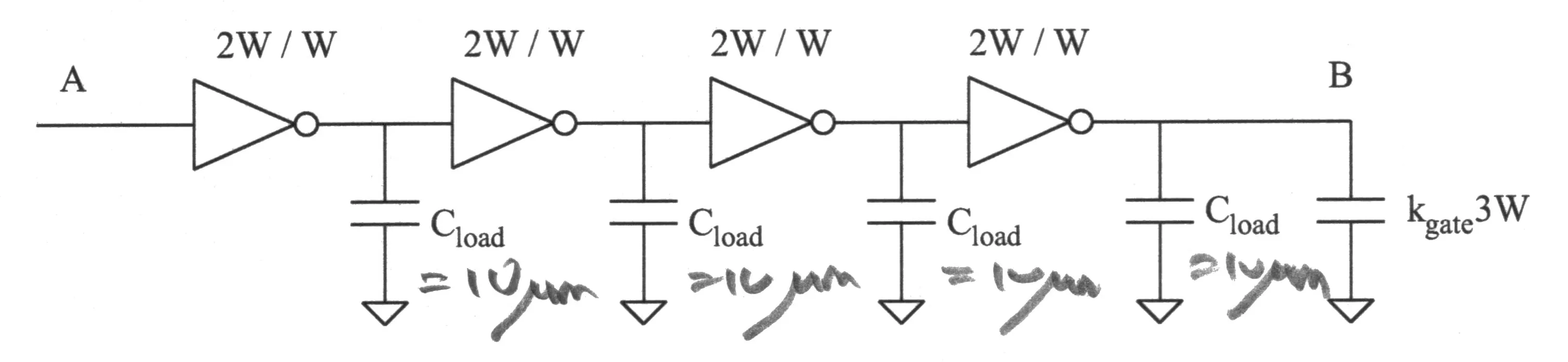
FN10-4, p6 (Fall 2010, 20 points). A chain of four identical inverters sized 2W/W “for a beta-ratio of one”, each loaded by . fF/µm; the FO1 delay is ps. The last output also carries .
A beta-ratio of one at 2W/W means equal rise and fall: , the balanced inverter, and . This is the MT17-4 chain (M3) with a number for the side load, so M3’s inverter-chain moves apply as they are.
FN10-4a: delay
FN10-4a, p6 (10 points). If fF and , what is the delay from A rising (falling) to B rising (falling)?
Hint
What it asks. The delay through four inverters, each output loaded by 20 fF, at m. “A rising to B rising” is right for four inversions, and with balanced inverters the falling case is the same.
The idea. This is MT17-4b with a number where MT17-4 had the symbol , so the electrical effort is a number too. Each stage is an inverter, , so its delay is , where is the node’s capacitance over the inverter’s own input (Chapter 7, Section 9). The convention matters here: a beta ratio of one at 2W/W makes rise and fall equal, and is the FO1 delay of exactly this inverter, so no is needed.
FN10-4a
- The node. Because every output drives the next inverter’s input and the side load: fF. In µm of gate (÷ 2 fF/µm): , where the 10 µm is the key’s handwritten “= 10 µm”.
- One stage. Because an inverter has , its gain is , and it takes ps. Rising and falling are equal, because the inverter is balanced.
- Four stages. Because the four identical stages switch one after another: ps.
Check. MT17-4b’s formula, , with fF: ps. ✓
Answer: 433 ps (each stage 108.3 ps).
Remember. Convert the side load to µm of gate (or keep both in fF), add the next input, and divide by one input: that is , and an inverter chain takes .
The answer key agrees
It prints 432 ps, from rounding each stage to 108 ps first; unrounded, ps.
FN10-4b: energy of one transition
FN10-4b, p6 (10 points). If fF and , what is the energy dissipated by a single transition through this inverter chain? Ignore leakage currents, crowbar currents and the energy introduced by the “source” at A. Consider only dynamic charging energy.
Hint
What it asks. The energy of one input edge through the chain, counting only the charging of the four nodes. “A single transition” decides the count: half the nodes rise.
The idea. This is MT17-4c with numbers. A rising node draws from the supply and a falling one draws nothing, so the energy is (the rising nodes) × (Chapter 6, Section 6). What is new: the question gives no , so write the energy with first and choose a value only at the end.
FN10-4b
- The node. Because the loads are those of (a), each of the four outputs carries 26 fF.
- Which nodes rise. Because each inverter inverts, one input edge makes two nodes rise and two fall.
- Price them. Because only a rising node draws from the supply, each, the two rising nodes draw ; counting dissipation instead, is the same.
- A number. Because the question gives no , take the key’s 2.5 V (“although any assumption is valid”): fJ.
Check. MT17-4c’s formula, , with fF and fF gives . ✓ Units: fF × V² = fJ.
Answer: , which is 325 fJ (0.325 pJ) at the key’s 2.5 V.
Remember. When the question gives no supply, answer with and then pick a value, saying so. Per transition, half the nodes rise.
The answer key agrees
It writes in 2.5 V by hand, “although any assumption is valid”.
What this means for the midterm
Which midterm family uses each method. The inverter below threshold has its own approach section; the chains follow M3’s.
- Off-current from a current at threshold (FN19-1a): is MT23-1b and MT24-2b (M3), MT17-1c with the temperature (M3) and M7’s Question 1. Below threshold, .
- Delay as charge over current (FN19-1c, FN17-10b, FN10-2b): . The midterms ask it in the RC form instead; the subthreshold version is the same idea with an exponential current.
- Chain delay with a fixed side load (FN19-3a, c, FN10-4a): with ; no finite delay optimum, energy × delay least where the gate load equals the side load. This is MT24-2c–e, MT23-1d, MT21-4a and MT17-4a–d (M3 §1–§4), and the formula sheet’s inverter-chain section.
- Energy per transition (FN19-3b, FN10-4b): for nodes, as MT21-4b and MT17-4c (M3); per cycle it is (MT23-1a, MT24-2a).
- A gate with stacks as a gain (FN19-3a): the stack rule gives , as in MT17-3d’s NAND4 (M3) and every path in M4.
Traps.
- Using the above-threshold law at a supply below (FN19-1b): it gives a negative current. Below threshold every current is on the exponential line.
- Delay to 50% against the full swing: a factor of 2 (FN17-10b’s key). Say which you use.
- Forgetting the series pair in a carry stage: each stage is with no load, not .
- “Minimize the delay” with a fixed load has no finite answer; with no fixed load the delay doesn’t depend on at all. Both are the answer the question wants, with the reason.
- Per transition against per cycle; and a the question never gave (FN10-4b): write the energy with and then pick a value if you must.
Time. Each of these parts is 2–4 minutes once the node capacitance (or the current) is written down. FN19-1 as a whole, 40 points, is about 12 minutes; FN19-3, 39 points, about 10.
What the keys get wrong
| Part | The key | Here |
|---|---|---|
| FN17-10b | each inverter : the full-swing time | the delay to 50% is half of it, (the FN10 key uses the ½) |
| FN10-4a | 432 ps | 433 ps (the key rounds each stage to 108 ps first) |
FN17-10a, FN10-2a–b and FN10-4b agree with their keys after re-solving. FN19 has no key; its answers here are this guide’s own. FN17-10c and FN10-2c are left out (see the top of the page).