24. Beyond bulk CMOS: SOI, FinFETs and gate-all-around
Lecture 23, the course’s last and shortest lecture, steps back from circuits to the transistor itself. For many generations, making chips better meant shrinking one structure: the planar bulk CMOS transistor, built in the top of a silicon wafer. Then, in the lecturer’s words, “the electrostatics of this device have gotten so poor that you simply can’t scale this geometry anymore, and you have to go to another kind of geometry” (01:24). The lecture walks through the structures that came instead, in roughly the order industry tried them. First silicon on insulator (SOI): an oxide under the device, first used to make chips resistant to radiation. Then partially depleted SOI, with its floating body. Then fully depleted SOI, with an ultra-thin body and a back gate. Then the problem that ended bulk scaling: a subthreshold slope that had grown from 60 to about 120 mV/decade. The FinFET fixed it by gating a thin fin of silicon from three sides, and gate-all-around nanowires take the same idea one step further. Every one of these structures, the lecturer stresses, was “actually done and sold by foundries”, and circuits were designed in it (01:50–02:00).
Background for the final. No past paper tests this lecture. Read it for the context of numbers the exam does use: the subthreshold slope, the body effect and device widths. Each section is short, with Checks and at most one light example built on the course’s own devices.
After this chapter you can:
- draw planar bulk CMOS and say which part of it SOI replaces, and why an insulator under the device stops most soft errors;
- tell a partially depleted from a fully depleted SOI device, and explain the floating body and its history effect;
- name PD-SOI’s two benefits (less source/drain capacitance, less body effect in a stack) and its price;
- explain how an FD-SOI back gate sets , and what a shift does to leakage;
- use to say by how many decades a device turns off, and why 120 mV/decade ended bulk scaling;
- explain why a FinFET restores the slope, and size a device in whole fins;
- say which capacitances a compact model leaves to extraction, and why a schematic simulation is optimistic;
- say what a gate-all-around transistor changes, and what limits scaling past it.
Boxes and equations marked board were written in the lecture. Parts marked added are explanations or examples this guide adds. Remarks about companies and nodes are the lecturer’s account at the time of the recording.
Symbols
| Symbol | Meaning | Unit | First appears |
|---|---|---|---|
| supply voltage | V | §1 | |
| , | the charge on a storage node and the node’s capacitance added | fC, fF | §1 |
| the electron charge, C | C | §1 | |
| acceptor doping of the p body | cm⁻³ | §2 | |
| Fermi potential of the body, | V | §2 | |
| thermal voltage, 25.85 mV at 300 K | mV | §2 | |
| the depletion depth under the gate at threshold | nm | §2 | |
| the thickness of the silicon film over the buried oxide added | nm | §2 | |
| the body’s potential added | V | §2 | |
| , | threshold voltage, and its value at | V | §3 |
| , | gate-to-source and source-to-body voltages | V | §3 |
| flat-band voltage | V | §3 | |
| gate-oxide capacitance per area | F/cm² | §3 | |
| depletion charge per area under the gate | C/cm² | §3 | |
| junction (diffusion) capacitance of a source or drain | fF | §3 | |
| , | a device’s current at (in this chapter’s plots) and at | A | §4 |
| subthreshold slope: the gate voltage for one decade of current | mV/decade | §4 | |
| the non-ideality factor in | — | §5 | |
| number of fins in a FinFET | — | §6 | |
| , , | a fin’s height, its thickness, and the fin pitch added | nm | §6 |
| effective width: the gated perimeter that carries current added | nm | §6 | |
| channel length | nm | §6 | |
| , , | path effort, stage gain and the inverter’s delay unit (Chapter 8) | —, —, ps | §6 |
| , | the number of nanowires in a stack, and the side of a square wire added | —, nm | §8 |
Notation trap. here is the fin’s thickness. This chapter writes temperature in words (“300 K”, “room temperature”), never as .
1. From bulk CMOS to silicon on insulator: radiation hardness and soft errors
You need
The planar NFET in cross-section (Chapter 9). Shallow trench isolation (STI), oxide-filled trenches, separates neighbouring devices. Between them sit the source and drain, and over the channel the gate on a thin oxide. The p body is the wafer itself, and a contact, the body tap, ties it to ground (Chapter 5).
A reverse-biased junction collects carriers (Chapter 3). The source and drain are –p junctions with the body, held at zero or reverse bias. Each has a depletion region with an electric field across it; an electron that wanders into that field is swept to the side, a hole to the p side.
A memory bit is a small charge (Chapter 19). An SRAM cell holds its bit as a voltage on a small internal node; if that node is pulled far enough the wrong way, the cell’s cross-coupled inverters latch the wrong value.
The question. What is “bulk CMOS”, why did a layer of insulator under the transistor first appear, and what does it protect against?
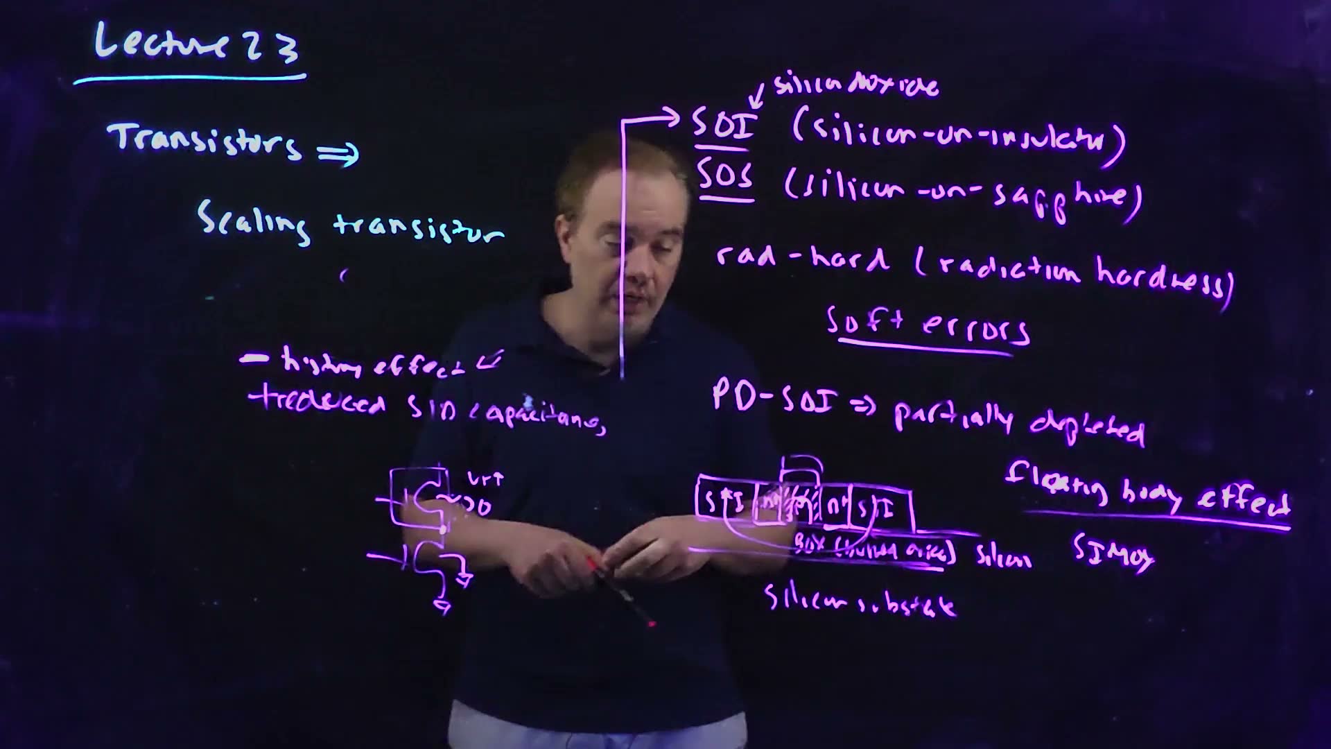
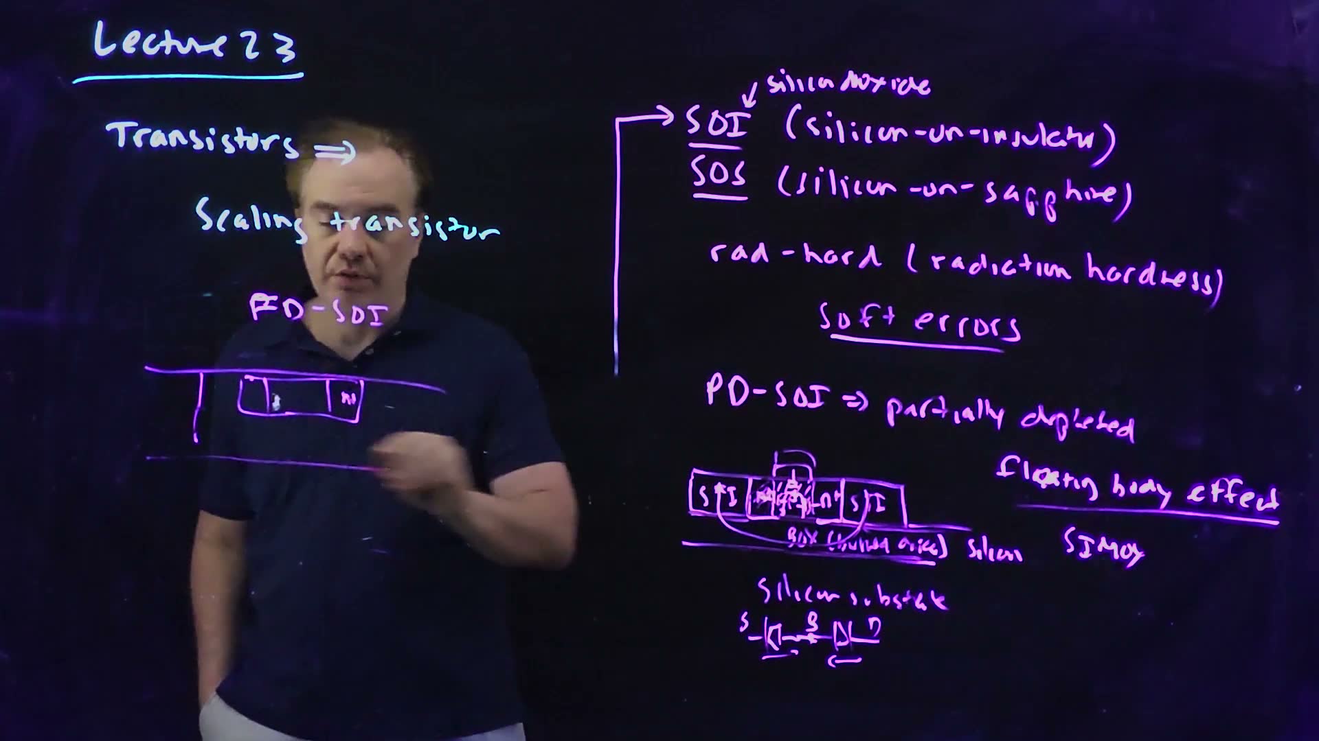
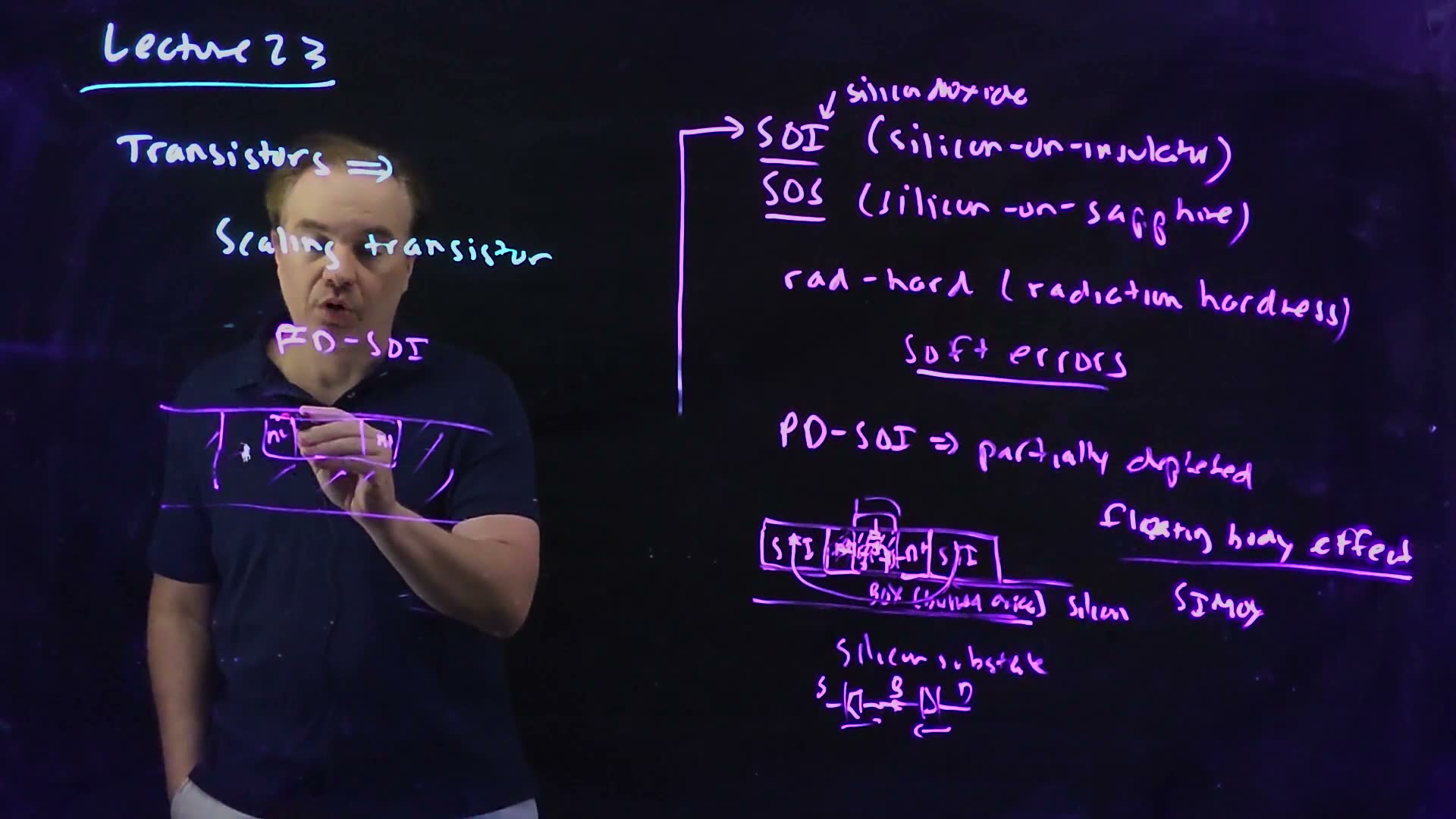
From bulk CMOS to SOI (board, 00:32–04:33)
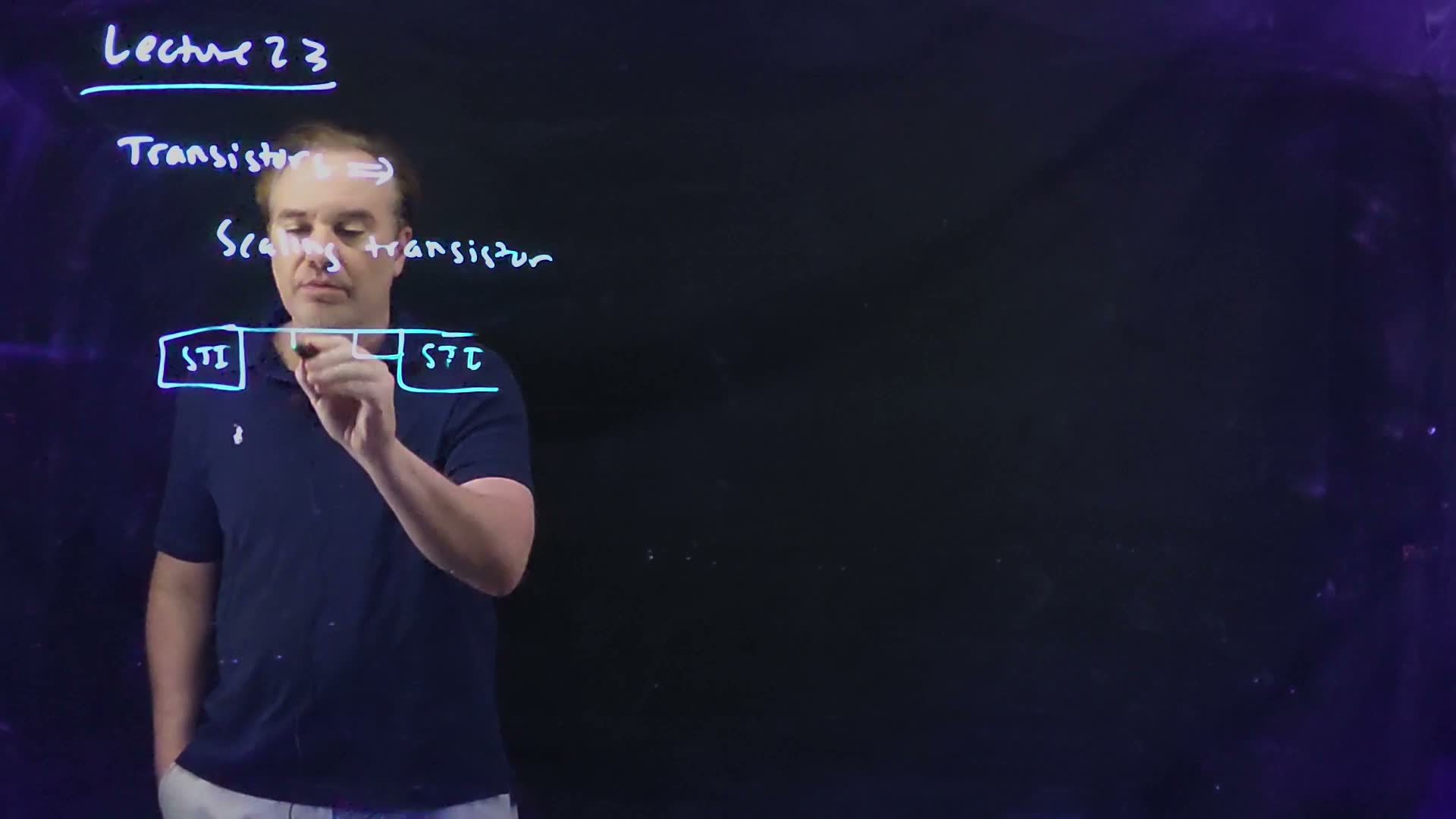
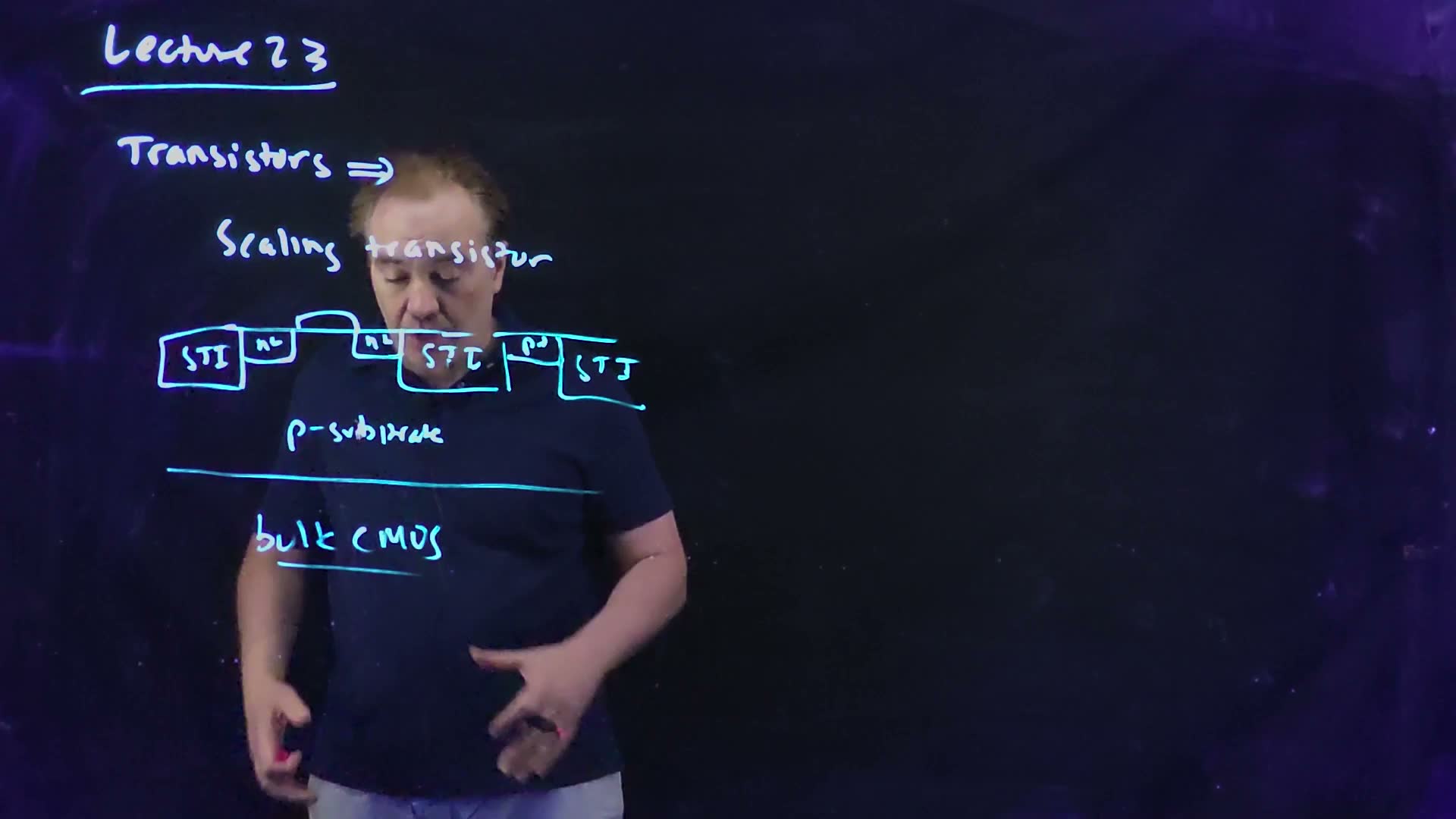
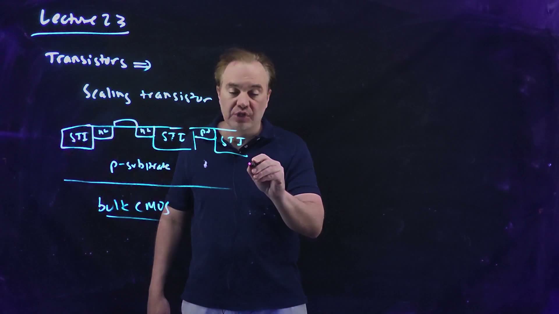
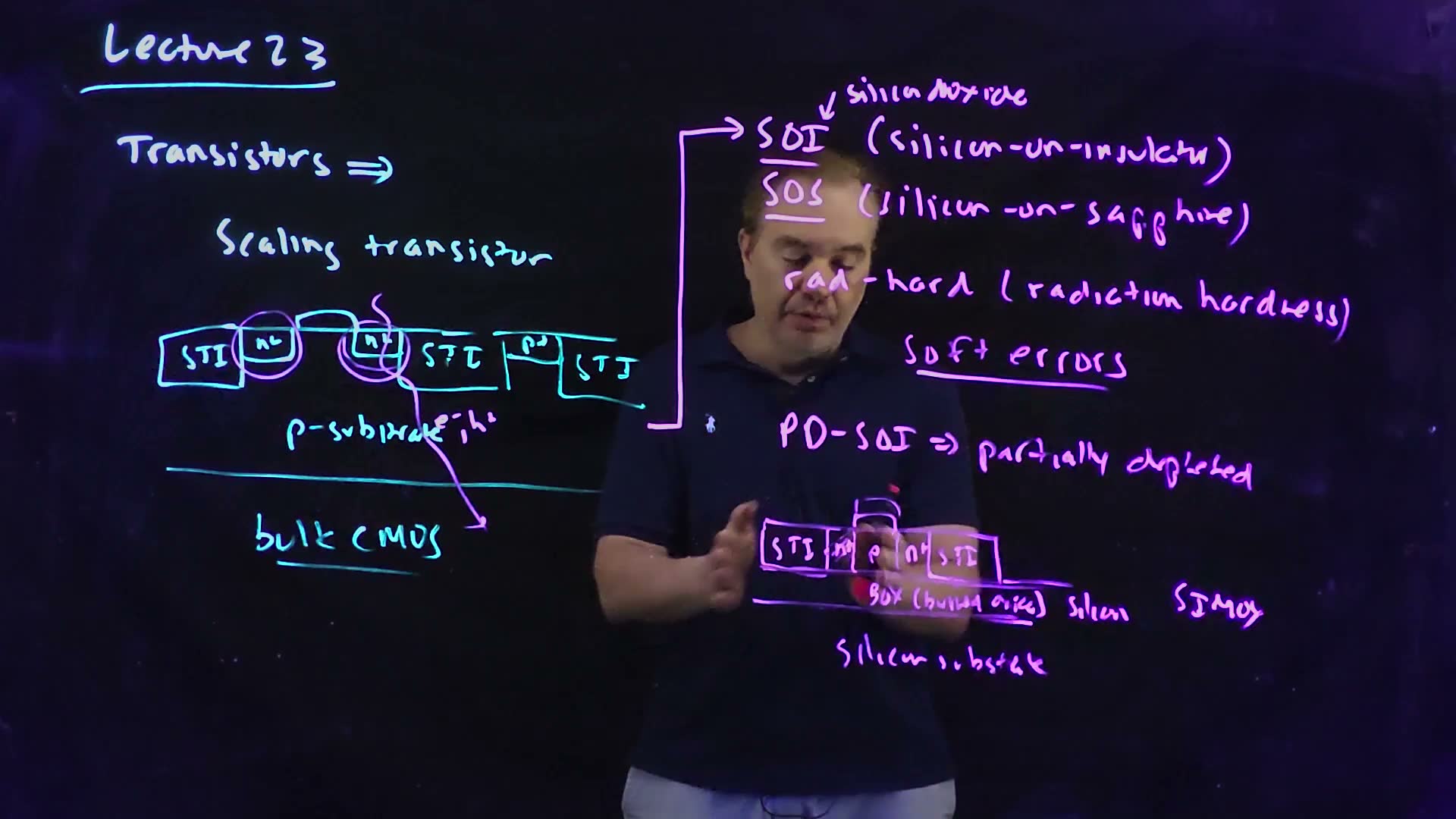
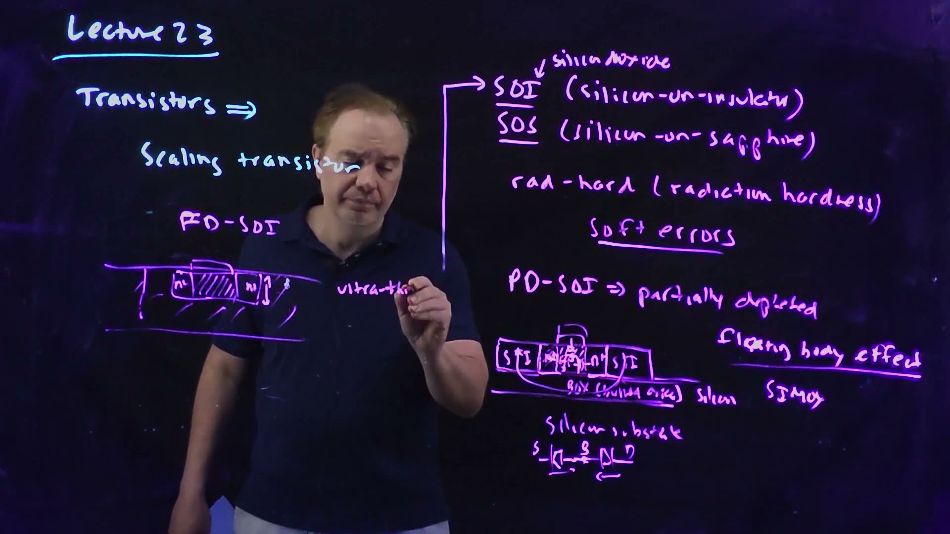
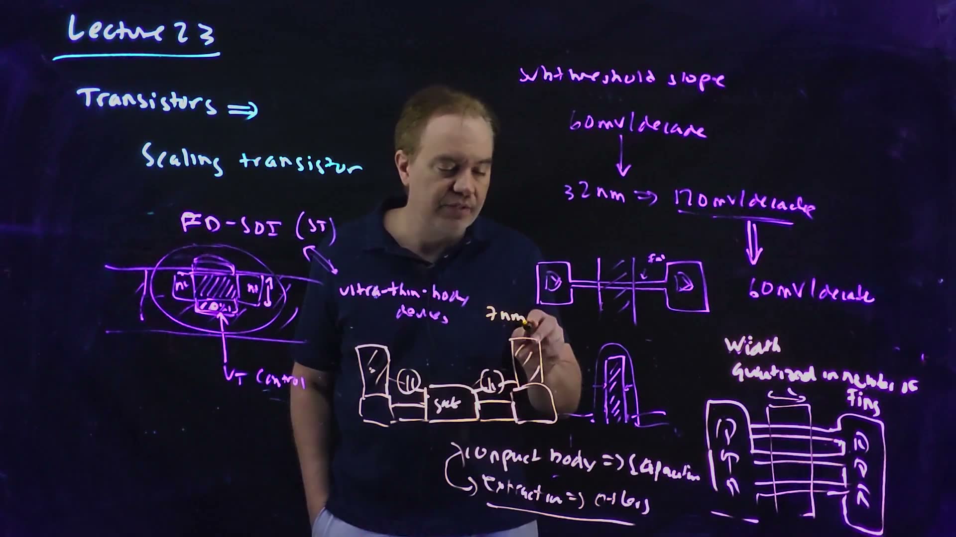
- Bulk CMOS board. The board draws the planar device: STI, , the gate, , STI, then a region between two more STI boxes, all in a p substrate that is “plugged and tied elsewhere” (00:40). The transistor is built in the top of a thick, uniform wafer: the “bulk”. The figure below redraws it.
- Scaling one structure. For many generations, technology development meant shrinking this one structure, with changes to its gate and dielectric materials along the way (01:09; the gate-dielectric story is Chapter 4 §13’s). Then the device’s electrostatics became too poor to keep shrinking it (01:24). Section 5 says what “poor electrostatics” means in numbers.
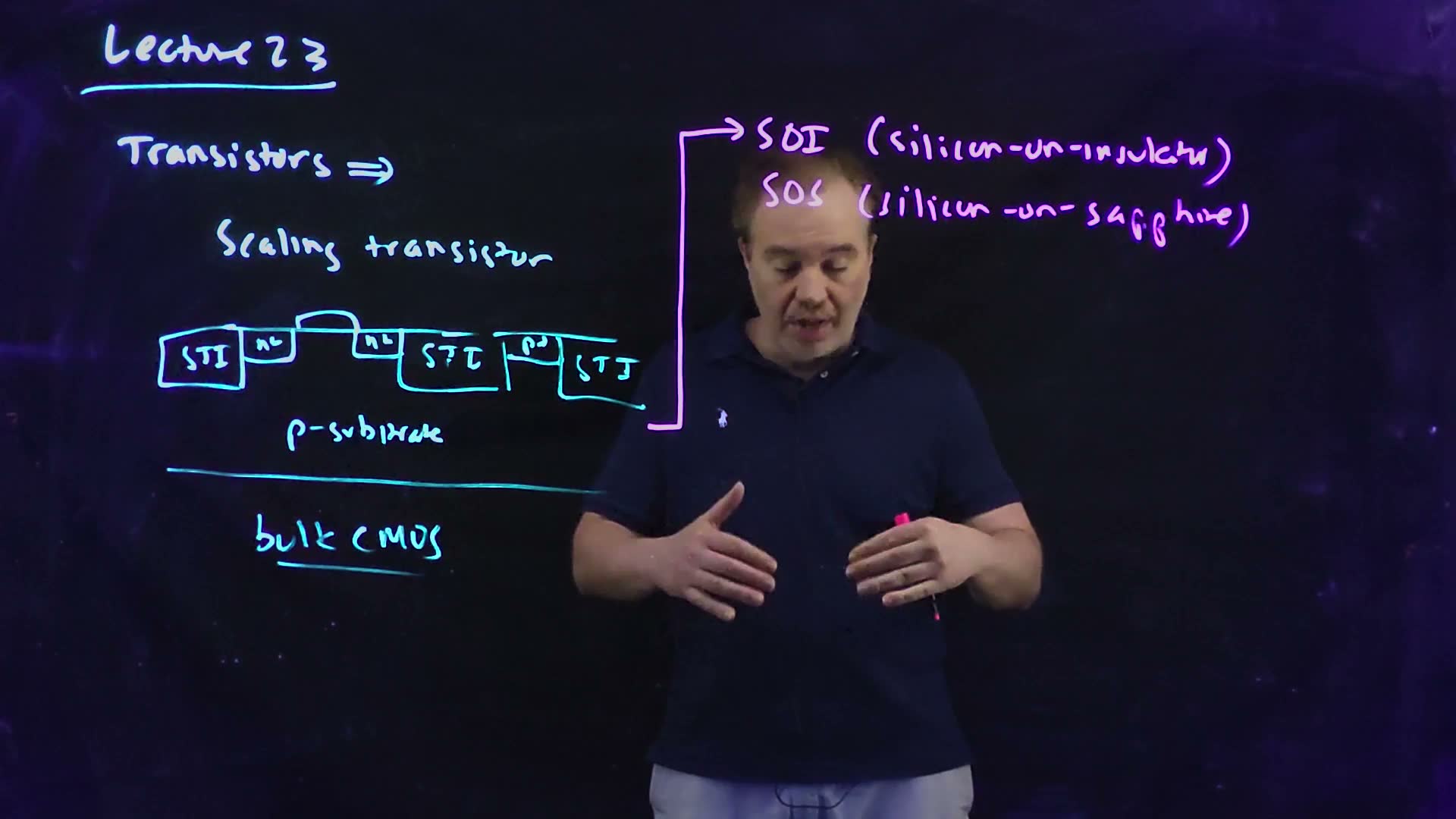
- SOS and SOI board. The first departure was to grow the silicon on an insulator. SOS, silicon on sapphire, grows a thin silicon layer epitaxially on sapphire, a very good insulator whose crystal lattice is close to silicon’s (02:39). SOI, silicon on insulator, generalizes it; the insulator is silicon dioxide (03:04; the board’s “silicon dioxide” with an arrow to the I).
- Rad-hard electronics board. Their first use was radiation-hard (“rad-hard”) electronics, for space, against soft errors (03:04–03:30).
- How a soft error happens board. Outside the atmosphere, a cosmic ray crosses the chip and leaves a track of electron–hole pairs behind it (03:30). In bulk silicon the track runs deep into the substrate, and the reverse-biased junctions nearby collect the carriers: the board’s wavy track through the drain and its “e⁻ h⁺”. Enough collected charge on a storage node flips a memory cell (03:56).
- Why an insulator helps. In SOI the device sits in a thin film over oxide. The track crosses very little silicon that is connected to the device, so little charge is generated where a junction can collect it, and few errors occur (04:05–04:33).
Planar bulk CMOS, redrawn from the board (Lecture23 @ 02:54). The transistor is built in the top of the p substrate (the bulk wafer); shallow-trench isolation (STI, grey) separates it from its neighbours, and the tap ties the body (B) to ground. The ground connection is added: the board says the substrate is “tied elsewhere”.
A soft error, after the board (Lecture23 @ 08:03) added. (a) In bulk, a particle’s track runs deep into the substrate and leaves electron–hole pairs all along it; the drain junction’s field collects the electrons onto the drain. (b) In SOI, the track crosses only the thin film; the pairs made under the buried oxide cannot reach the device. The board’s track is wavy; it is drawn straight here.
How much charge is a bit? added A storage node of capacitance at voltage holds ; dividing by counts the electrons. For example, a 1 fF node at 1.0 V holds 1.0 fC, about 6,242 electrons; a smaller node of 0.5 fF at 0.8 V holds 0.40 fC, about 2,497. A particle that frees a few thousand electrons near the node’s junction can be enough to upset it, if the junction collects a large share of them, and every new technology makes the node smaller. (Illustrative values, “for example”.)
Traps.
- “A soft error is a defect.” The cell is not damaged; it holds the wrong bit, and the next write fixes it. That is what “soft” means.
- “SOI has no junctions.” The source and drain junctions remain, at the sides of the film; what is gone is the deep collecting volume under them.
Check yourself Why is a cell less likely to flip in SOI than in bulk, for the same particle?
The particle frees charge all along its track, but only carriers in silicon connected to the device can be collected by its junctions. In bulk that is the whole depth of the track through the substrate; in SOI it is only the short stretch through the thin film, because the buried oxide cuts the device off from the substrate. Less collected charge, fewer flips.
Check yourself A storage node holds 0.8 fF at 0.9 V. How many electrons does it store, and would a particle that frees 2,000 electrons at its junction be a concern?
0.72 fC, and 4,494 electrons. A particle that frees 2,000 electrons there is of the same order: if a large share is collected, it can pull the node far enough to flip the cell. Yes, a concern.
Check yourself What did SOS use as its insulator, and what does SOI use?
SOS grows the silicon on sapphire (an insulator whose lattice is close to silicon’s); SOI puts it on silicon dioxide.
2. Partially depleted SOI: the buried oxide and the floating body
You need
The depletion depth at threshold (Chapter 3). With a positive gate voltage, the p body under the gate is depleted of holes to a depth that grows until the channel forms. At threshold the surface has bent by , and the depth is at its maximum:
for a uniformly doped body, in the depletion approximation ( for silicon, cm⁻³, = 25.85 mV at 300 K).
The body tie in bulk. In bulk CMOS the tap holds the body at ground:
A junction leaks in reverse and conducts forward (Chapter 2). A reverse-biased pn junction passes a tiny leakage current; forward-biased by more than a few tenths of a volt, it conducts strongly.
A floating node follows its capacitors (Chapter 21). A node with no DC path is moved by the capacitors joining it to its neighbours: when a neighbour steps, the node steps by a capacitive-divider share.
The question. What does a practical SOI transistor look like, how are its wafers made, and what happens to its body when there is no tap to tie it?
PD-SOI and its floating body (board, 04:42–08:55 and 11:40–12:46)
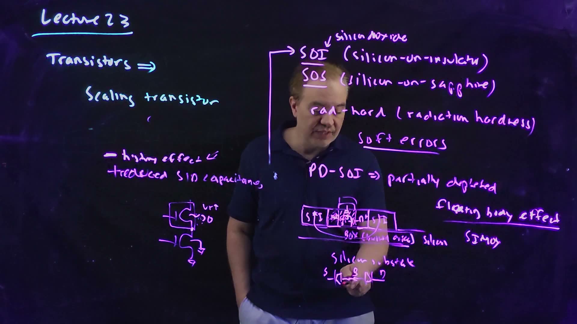
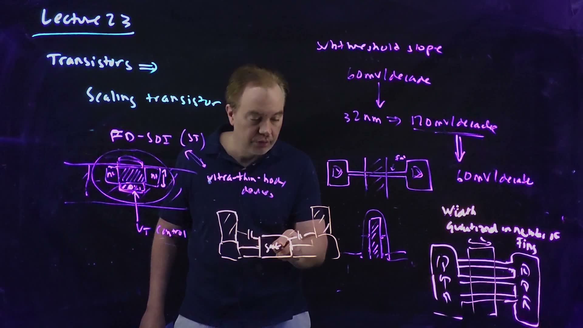
- PD-SOI board. “PD-SOI ⇒ partially depleted” (04:42). IBM pushed this technology from the mid-to-late 1990s, as the lecturer recalls (05:01).
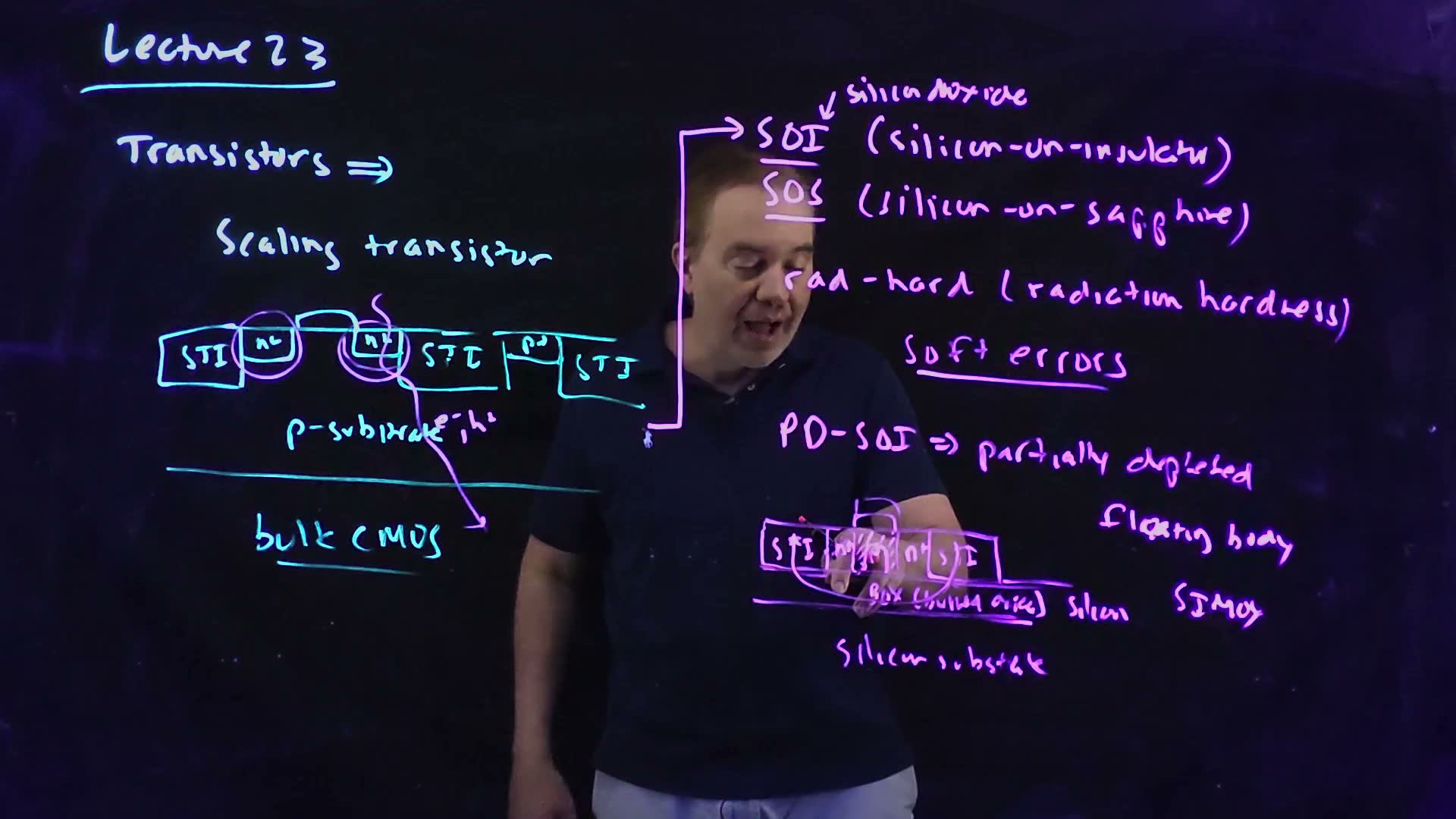
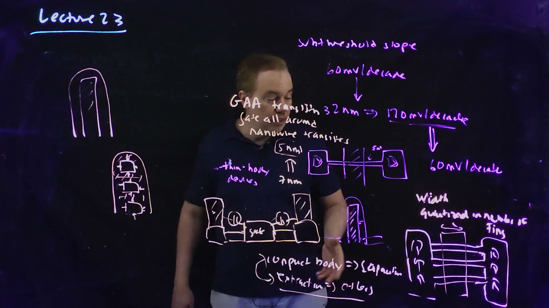
- The buried oxide board. The device sits on a BOX, a buried oxide, over the silicon substrate: STI, source, the p body (hatched on the board), drain, STI, with oxide on all sides (05:21–06:00).
- Making the BOX. Two ways (06:00–06:59). SIMOX board: implant oxygen deep into an ordinary wafer, then anneal out the damage. (The name stands for separation by implantation of oxygen added; the lecturer did not recall it.) Or bonded wafers: grow oxide on two wafers, bond them oxide to oxide, and etch one back down to a thin film, stopping at an etch stop. Bonding gives better silicon, and the lecturer saw it used for most SOI wafers.
- The body floats. With oxide below and STI at the sides, there is nowhere to put a body tap: the body is “not connected to any known potential” (07:28). It is a floating body board. Compare the bulk device of Section 1, whose tap holds it at ground.
- Why “partially depleted”. The depletion region under the gate does not reach the BOX, so a neutral p region remains between them (07:59). That neutral region has a potential: the body potential . It is real, but nothing sets it.
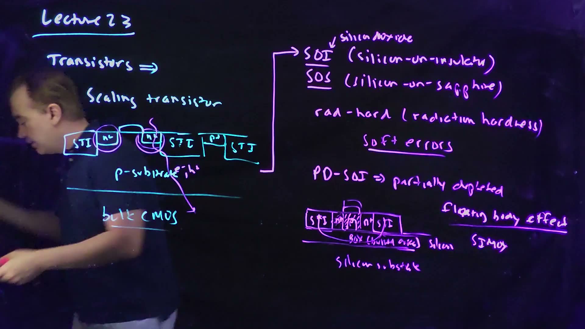
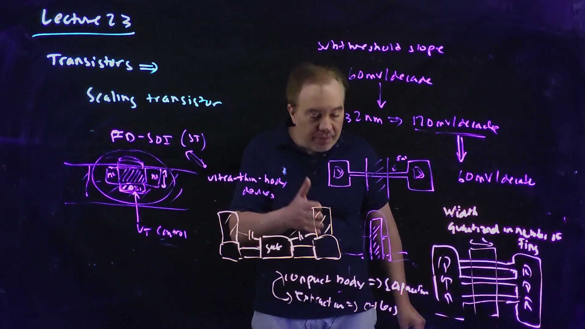
- What does set it (11:40–12:45). Two things. Capacitive coupling to the gate, source and drain moves the body potential without changing its charge. Two diodes, body to source and body to drain (the board’s “S —⊳|— B —|⊲— D”, anodes at B), change the charge: in reverse bias they leak, slowly charging the body; forward-biased, they “would immediately turn on and drain any charge”. Hold the source and drain at long enough, and the body rises toward too.
- The floating body effect board. So the body bias depends on what the transistor did before: “There’s an additional history dependence in the way this transistor operates. It has memory” (08:29). Designers were unwilling to accept that uncertainty, which is one reason PD-SOI never spread widely.
Partially depleted SOI, redrawn from the board (Lecture23 @ 09:15). The device sits on the buried oxide (BOX) over the silicon substrate (Si), with STI at its sides. The depletion region under the gate (dotted edge) stops short of the BOX, leaving a neutral body B (shaded, added) with no tap: the floating body.
The board (Lecture23 @ 08:48)
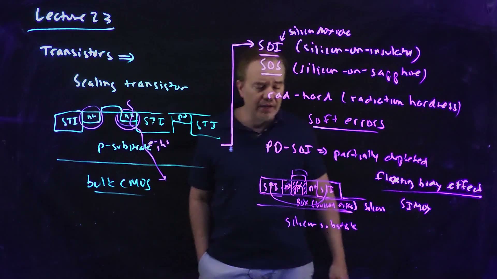
Fair copy of the board above (Lecture23 @ 08:48), mark for mark in its own layout, all in black. A white pen wrote the title and the two lines under it; a cyan pen drew the bulk device; a violet pen wrote everything from SOI on, and also the soft-error marks over the bulk drawing: the rings round both n⁺ regions, the particle track and “e⁻ h⁺”. The violet pen carries the lecture on to SOI rather than marking a separate layer, so it takes no accent. The “r” of “rad-hard”, washed out by the lecturer’s face, and the middle of the PD-SOI row, under his arm, are read from 09:15, where nothing has changed. The hand’s last “STI” ends in a hook that reads like “STJ”. The labels inside the PD-SOI row are set smaller than the hand.
What sets a floating body’s potential, from the board (Lecture23 @ 12:46) and the speech. The two body diodes (the board’s, anodes at B) change the body’s charge: their reverse leakage slowly charges it, and a forward bias drains it at once. The capacitors to G, S and D (grey, with dashed wires: spoken at 11:40, not drawn) move its potential without changing its charge.
The board (Lecture23 @ 12:46)
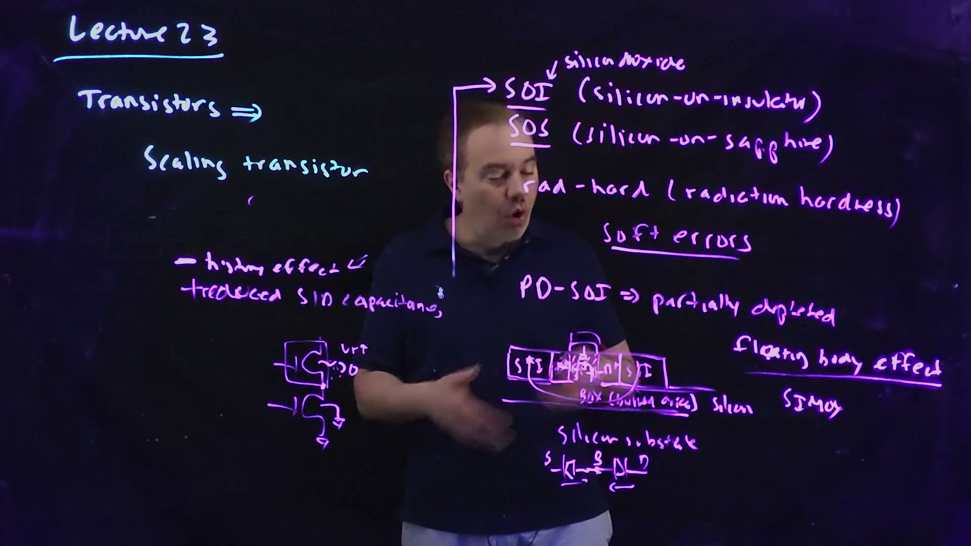
Fair copy of the board above (Lecture23 @ 12:46), mark for mark in its own layout, all in black: one violet pen wrote everything new; the title and the two lines under it are the opening board’s white pen. The right half is 08:48’s, copied from the same marks; the bulk drawing and the bracket’s foot are wiped, and two tiny stroke ends left of the bulk drawing are left out. The middle of the PD-SOI row, under the lecturer’s hand, is read from 13:31; the tick above the gate is new by 12:18. The stack’s label, beside the hand, is read from 12:18: a short wavy line from the body, then ↑ and “> 0”: the body floats above ground (10:39–11:14). The hand’s “+” before “reduced” has a tail and looks like a “t”. The diodes, new at 12:46, are the body’s two junctions to the source and the drain.
PD or FD: compare the film with the depletion depth. added The depletion region can be no deeper than . If the silicon film is thicker (), a neutral body is left over it: partially depleted. If the film is thinner (), the depletion reaches the BOX first and no neutral body is left: fully depleted (Section 4).
Derive it in one line: the depletion stops either at or at the BOX, whichever comes first.
A worked example: Chapter 3's body in a film (added; films for example)
- The body. Chapter 3’s NFET, cm⁻³: 0.833 V.
- The depth. cm 103.8 nm.
- A 150 nm film. It is thicker than 103.8 nm, so 46.2 nm of neutral body is left under the depletion: PD.
- Heavier doping. At cm⁻³, 0.952 V and 35.1 nm: the depletion is ten times denser in charge and only about a third as deep.
Traps.
- “Floating” means “at zero”. It drifts with the history, and on average sits above ground (Section 3).
- “The body diodes act only when forward-biased.” Their reverse leakage is exactly what charges the body, slowly.
Check yourself Why does a PD-SOI body have a potential at all, and an FD-SOI body none?
In PD-SOI the depletion region stops above the BOX, so a neutral p region is left, and a neutral region has a well-defined potential: the body potential, set by coupling and the two diodes. In FD-SOI the film is depleted all the way through; there is no neutral region, so there is no body whose potential could float.
Check yourself A PD-SOI NFET's source and drain both sit at VDD for a long time. Which diodes act, in which direction, and where does the body end up?
Both diodes (body to source, body to drain) are reverse-biased, since the body starts below ; their reverse leakage carries charge into the body. Nothing drains it (a diode would only conduct if the body went above ), so the body rises slowly toward , as the lecturer says (12:45).
Check yourself At NA = 1018 cm−3, is a 50 nm film partially or fully depleted?
Partially: = 35.1 nm at that doping, and the 50 nm film is thicker, so 14.9 nm of neutral body is left.
3. What PD-SOI buys: less junction capacitance, less body effect
You need
Junction capacitance (Chapter 5). The source and drain are reverse-biased junctions with the body, so each is a capacitor, per area of junction ( the depletion width). In bulk the junction has a bottom (the area under the diffusion) and sidewalls (its perimeter); both count.
The body effect (Chapter 5). If the source sits above the body (with , so the source junction stays off), the depletion under the gate must hold , and
In a stack of two NFETs with grounded bodies, the upper device’s source is the middle node, above ground, so its rises and its overdrive falls. Chapter 5’s example: source at 1 V, = 1 V, rises from 0.500 V to 0.626 V.
PD-SOI (Section 2). The device sits on a buried oxide; its body floats.
The question. PD-SOI’s floating body made designers uneasy. What did it offer in return?
Two benefits and a price (board, 12:18)
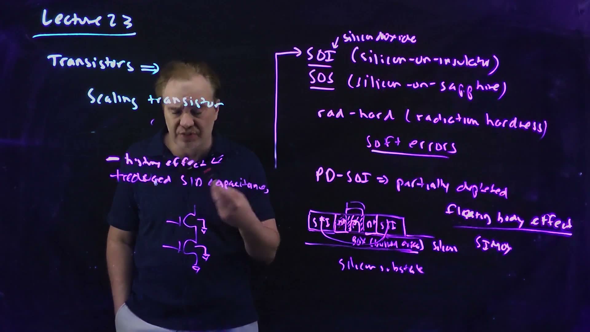
- Reduced S/D capacitance board. The board’s “+ reduced S/D capacitance” (12:18). The source and drain diffusions are now “surrounded on these sides by oxide”, so their capacitance “decreases dramatically” (09:00–10:02). added They reach down to the BOX, so the bottom junction against the body, usually the larger part, is gone; the sidewall facing the body under the gate remains, so the junction capacitance falls a lot but not to zero.
- The stack in bulk. In a stack, the upper NFET’s source is the middle node, above ground, while its body is tied to ground: it sees a positive , its threshold is pushed up, and it switches more slowly (10:09–10:39). The body effect is weaker in scaled devices, but “there still is a body effect”.
- The stack in PD-SOI. The upper device’s body is not tied. It floats, and “tends to float up”, on average above ground (the board’s “ ↑ > 0” beside the boxed device). Its is smaller, so its body effect is smaller and it switches better, “theoretically” (10:39–11:14).
- The price board. “− history effect”: the body potential, and so , depends on what the device did before (Section 2).
Where the junction capacitance goes added (after the board’s “+ reduced S/D capacitance”, Lecture23 @ 12:18). (a) In bulk the drain meets the p body along its bottom and its channel-side wall (thick, with the dotted depletion edge); both carry , while its STI side is oxide. (b) In PD-SOI the drain reaches the BOX, so the bottom is oxide; only the sidewall facing the body is left.
The stack’s upper device, redrawn from the board (Lecture23 @ 12:18). (a) In bulk both bodies are tied to ground, so the upper device sees , the middle node’s voltage. (b) In PD-SOI the bodies float; the upper body rises above ground (), so is smaller. is added.
A worked example: Chapter 5's stack with a floating body (added; body voltages for example)
- The device. Chapter 5’s NFET ( cm⁻³, = 5.4 nm, = 0.500 V) as the upper device of a stack, its source at 1 V and its gate at 2.5 V, so = 1.5 V.
- Bulk. The body is tied at 0 V: = 1.0 V, so 0.626 V and the overdrive is 0.874 V.
- PD-SOI, body at 0.3 V. V, so 0.593 V and the overdrive is 0.907 V.
- PD-SOI, body at 0.5 V. = 0.5 V, 0.569 V, overdrive 0.931 V: 6.5 % more than in bulk.
- The catch. The body’s 0.3 V or 0.5 V is not a design value: it depends on the history. That uncertainty is the history effect.
Traps.
- “The floating body always helps.” It varies with history, so the delay becomes uncertain; a timing check needs both ends of the range.
- “SOI has no junction capacitance.” The sidewall to the body remains.
Check yourself Which part of the drain's junction capacitance does the BOX remove, and which remains?
It removes the bottom junction: the drain now stands on oxide, not on p silicon. The sidewall facing the body under the gate is still a junction, so its capacitance remains.
Check yourself In the worked example's stack, the floating body of the upper device sits at 0.2 V. What is its VSB, and is its VT above or below the bulk device's 0.626 V?
0.8 V. Then 0.604 V, below the bulk device’s 0.626 V: the smaller means less body effect.
Check yourself Why would a designer distrust a delay that depends on what the gate did a microsecond ago?
Static timing checks each path once, at its worst case. If a device’s moves with its switching history, the worst case depends on the input sequence, which no single analysis covers; the designer must margin for the whole range, and so loses part of the gain.
4. Fully depleted SOI: the ultra-thin body and the back gate
You need
PD or FD (Section 2). A film thicker than the depletion depth keeps a neutral, floating body (PD); a thinner one is depleted through (FD).
The threshold (Chapter 3). : the flat-band voltage , set mainly by the gate’s work function (Chapter 3); the band bending ; and the depletion charge over the oxide capacitance.
The subthreshold line (Chapter 4). Below threshold the current falls tenfold for every volts the gate goes below ; is the subthreshold slope, about 60 mV/decade at best.
The question. What if the film is so thin that there is no body at all? What then sets the threshold, and what can a second gate under the film do?
FD-SOI (board, 12:53–15:52)
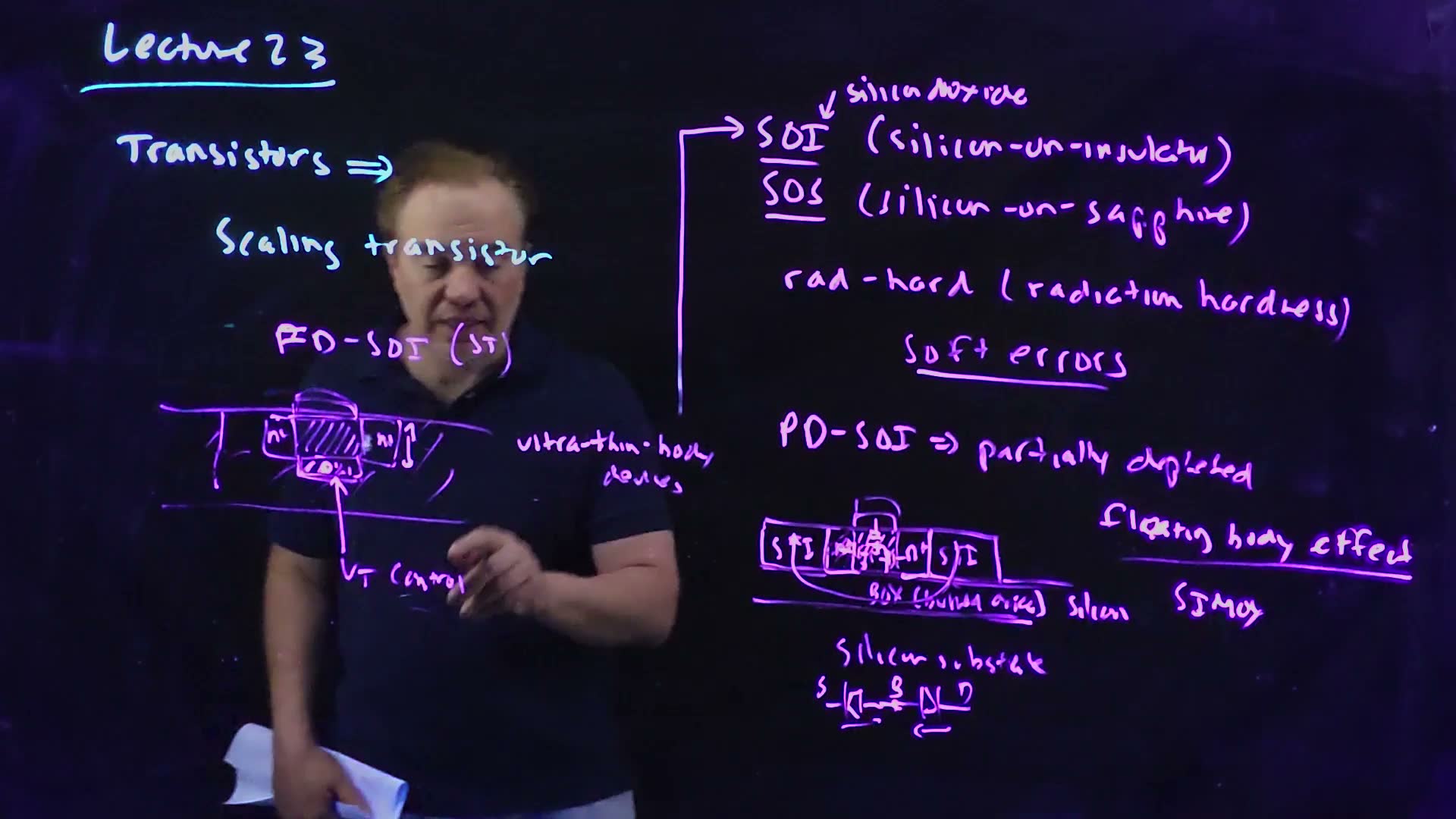
- FD-SOI board. Fully depleted SOI: the same device on oxide, but its film is undoped or only lightly doped, and thin, so it is depleted all the way through (12:53–13:34). There is no neutral region and no body potential: the lecturer calls it “a three-terminal transistor” (07:59). So there is no floating body effect.
- What sets . With no body, the threshold “is entirely determined by the electrostatics, the work function, and more importantly by the exact thickness” of the film (13:34–14:14).
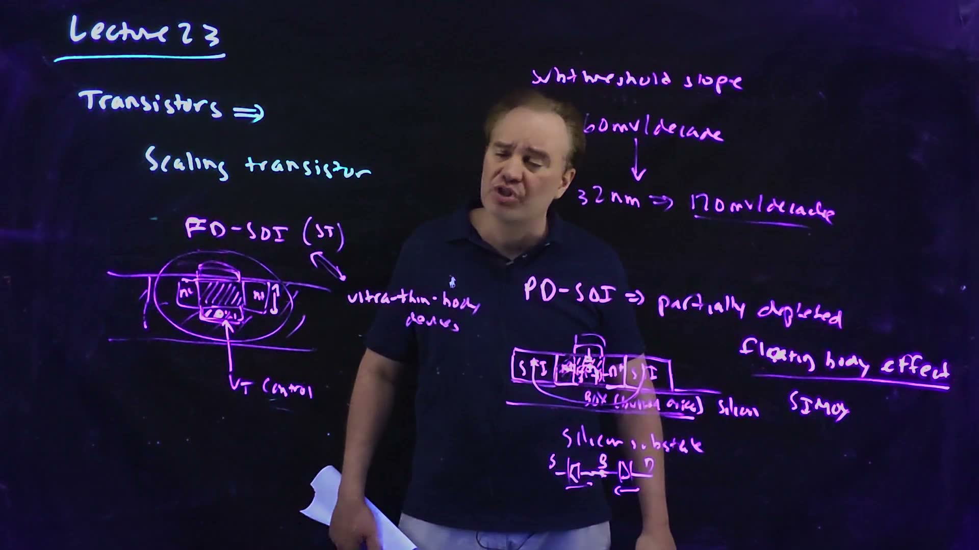
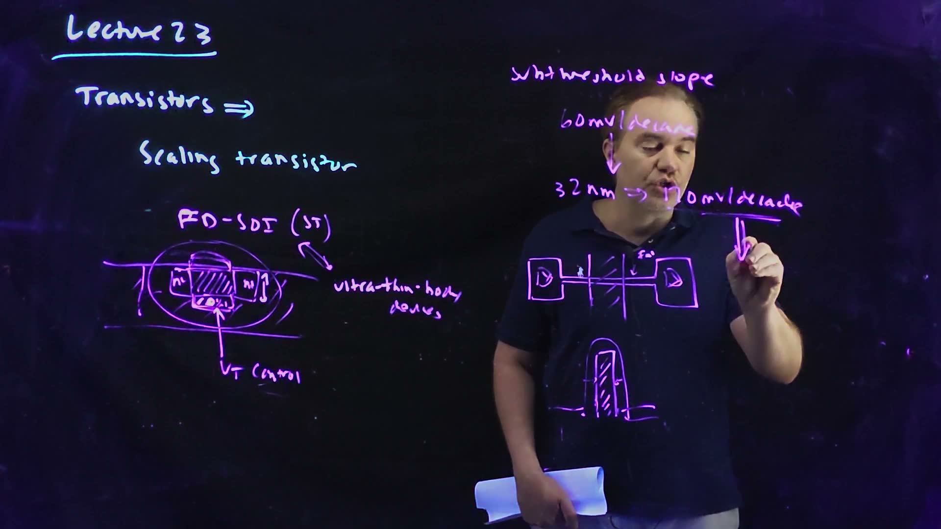
- Ultra-thin body board. These are ultra-thin-body devices (14:14). ST was making them at the time (the board’s “FD-SOI (ST)”).
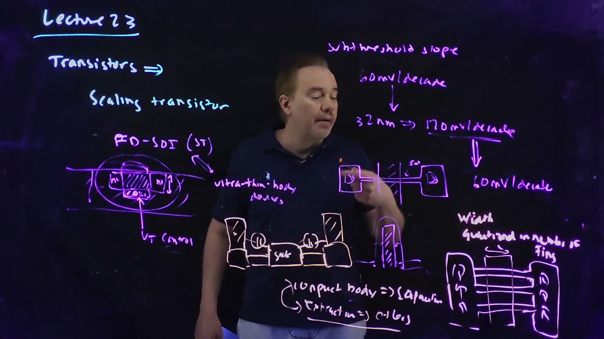
- The back gate board. Under the film, inside the buried oxide, a conducting back gate: heavily doped silicon, for example, though the lecturer did not recall the material (14:27). The back gate sets (the board’s “ control”); the top gate switches the device (14:53).
- What it is for. Ultra-low-power chips: in standby, raise through the back gate and shut off the leakage (15:22).
- The turn. These SOI variants offered “extra functionality”. Meanwhile scaling was running into a more fundamental problem (15:52): Section 5.
Fully depleted SOI with a back gate, redrawn from the board (Lecture23 @ 15:24). The film, of thickness , is depleted through: there is no neutral body. A back gate (BG, label added; the board’s label is unclear) buried in the oxide under the film sets the threshold (the board’s “ control”); the top gate switches.
The board (Lecture23 @ 16:05)
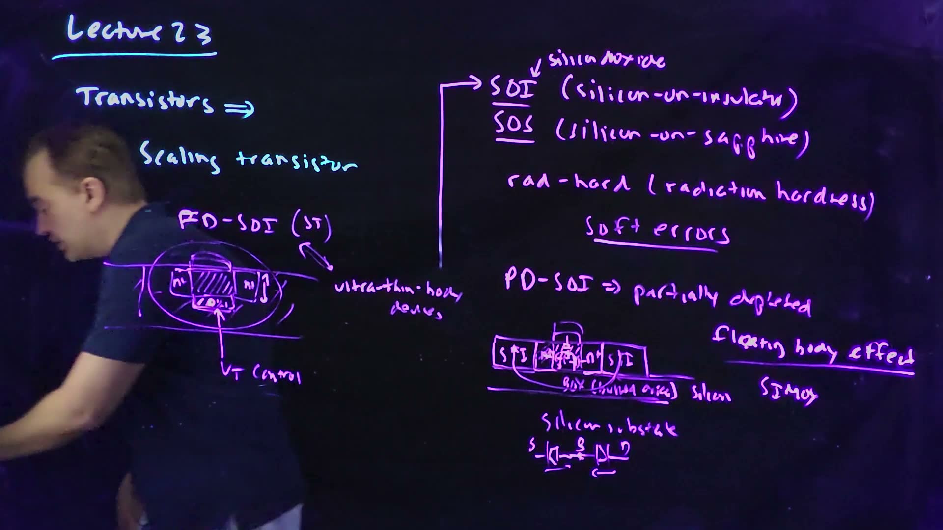
Fair copy of the board above (Lecture23 @ 16:05), mark for mark in its own layout, all in black: one violet pen wrote everything new; the title and the two lines under it are the opening board’s white pen. The right half is 12:46’s, copied from the same marks. “History effect”, “reduced S/D capacitance” and the stack are wiped by 13:31. The “F” of “FD-SOI” is written over a “P”. The lecturer bends at the far left but covers no stroke (checked against 15:24). The back gate’s label is unclear, so it is copied as its strokes, two small loops and two ticks; the speech calls the back gate conducting, for example “heavily doped silicon”, and the lecturer is unsure what material is used (14:27–14:53).
Why the doping drops out added. In Chapter 3’s formula the depletion term is . In a fully depleted film the depletion charge can be no more than the film holds, per area. For a thin, lightly doped film that term is tiny, so the threshold rests on , that is, on the gate’s work function. The film’s thickness matters through the electrostatics of the thin body, which is the lecturer’s stronger claim; this chapter quotes it rather than deriving it.
How much a shift buys added. Below threshold, every volts of is a decade of leakage at , so raising by divides by . The same arithmetic sizes the high- header of Chapter 23 §12.
Derive it: (the subthreshold line evaluated at ); divide the two.
A worked example: the film's charge and the back gate's knob (added; values for example)
- The bulk device’s depletion term. Chapter 5’s NFET ( cm⁻³, F/cm²): 0.260 V of its 0.500 V threshold.
- The same doping in a 10 nm film. The most the film can hold is C/cm², and over that is 25.1 mV; a 7 nm film, 17.5 mV. The work function now carries the threshold.
- A back gate that raises by 100 mV. The leakage falls by : ÷34.6 at 65 mV/decade, ÷12.9 at 90, ÷6.8 at 120. A steep slope makes the back gate a strong knob.
Traps.
- “Set an FD device’s by its doping, as in bulk.” With no body there is no -and-doping recipe: the work function and the film’s thickness set it.
- “The back gate is Chapter 5’s body bias.” There is no body to bias; the back gate acts through the oxide on the depleted film, as a second, weaker gate.
Check yourself Why is there no floating body effect in FD-SOI?
The film is depleted all the way to the BOX, so no neutral region is left. A floating body effect needs a neutral body whose potential can drift with history; here there is none.
Check yourself In standby, a back gate raises VT by 150 mV on a device with S = 75 mV/decade. By what factor does the leakage fall, and how much VT shift would the same factor need at 120 mV/decade?
: the leakage falls 100 times. At 120 mV/decade, two decades need 240 mV of shift: a poor slope makes every knob on weaker.
Check yourself Why does the lecture say the film's thickness matters more than its doping?
In a thin film the depletion charge is capped by what the film holds, , a few tens of millivolts of threshold at most, so the doping hardly moves . What remains is the gate’s work function and the electrostatics of a thin body, which change with its exact thickness.
5. The subthreshold slope: why bulk CMOS ended
You need
The subthreshold current (Chapter 4). Below threshold a MOSFET still conducts: carriers cross the source’s barrier thermally, so . On a log scale that is a straight line in , and the gate voltage for one decade of current is the subthreshold slope
59.5 mV/decade at and 300 K: about 60, the floor for a barrier crossed thermally. Real devices have , because the gate does not control the barrier perfectly.
Short-channel effects (Chapter 4). In a short device the drain’s depletion region reaches under the gate and lowers the barrier (DIBL): the gate controls less of the barrier, the output conductance worsens, and the slope flattens.
The question. What happened to the subthreshold slope as bulk devices shrank, what does a slope of 120 mV/decade do to leakage and to the threshold a chip can use, and why did that force new structures?
From 60 to 120 mV/decade (board, 16:25–17:50)
- Bad electrostatics, first sign. Short-channel effects: an output conductance “that gets terrible” (16:25).
- The ideal board. “Ideally the subthreshold slope at room temperature would be 60 millivolts per decade” (16:41).
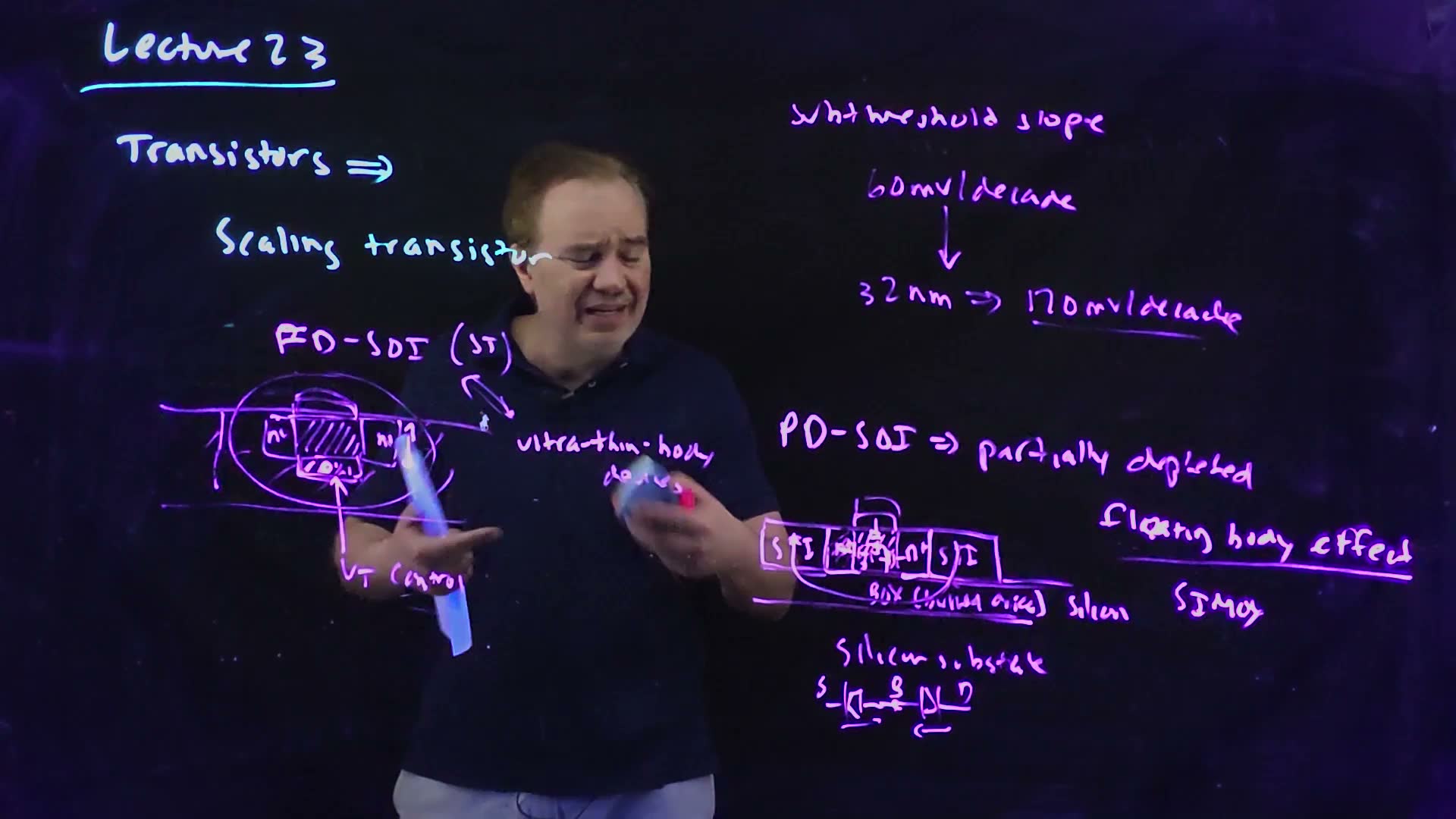
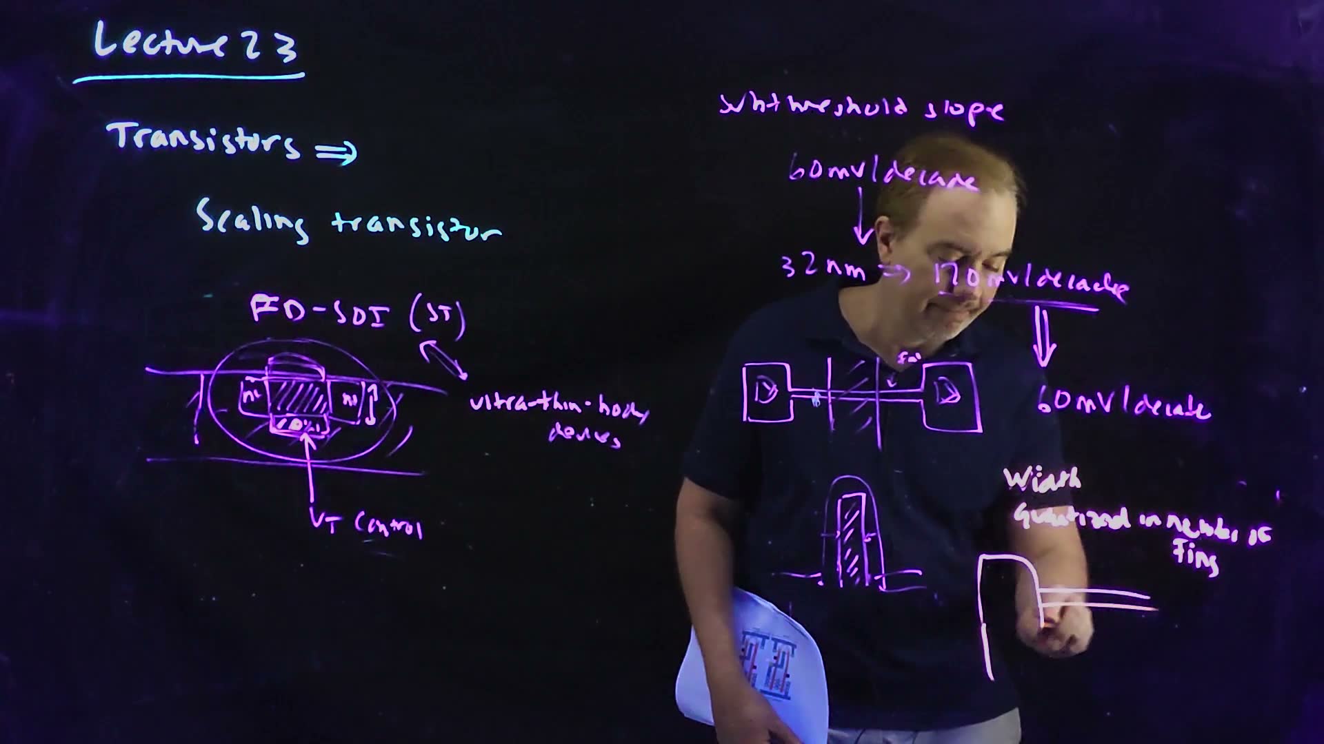
- The end of bulk board. “At about the 32 nanometer node, which was the sort of the end of bulk CMOS, this had creeped up to about 120 millivolts per decade. So almost a factor of two worse” (16:47). The board writes “32 nm ⇒ 120 mV/decade” under the 60.
- What it costs. “Horrendous subthreshold leakage”, and further scaling would only make it worse (17:17). The worked example below puts numbers on it.
- The way out. So “people went back” to thin bodies gated on more than one side, like the FD-SOI device of Section 4 with its back gate, and looked for an area-efficient version of that idea (17:17–17:50): the FinFET, Section 6.
Other numbers in this guide added. Chapter 4, from Lecture 4’s board, says bulk reached about 100 mV/decade at the 22 nm node and calls 80–100 typical; the past papers state 80 (FN10-2, FN12-1, FN17-10) or 90 (FN19-1, MT23-1b). The two lectures give round numbers for the same story, and the chapter quotes each as said. In terms of , 120 mV/decade is 2.0 (100 is 1.68).
What the slope does: decades of turn-off added. On the subthreshold line, going from down to lowers the gate by , which is decades. So a device’s turn-off ratio, from its current at to its leakage at zero, is . With the same and the same on-point, a flatter slope leaks more.
Derive it: falls by per volt of ; over volts it falls decades. The second form divides two such lines that share the on-point.
The subthreshold slope sets the turn-off added, computed from with = 0.3 V and = 60, 90 and 120 mV/decade. All three lines share the on-point at ; at they are 5, 3.33 and 2.5 decades down, so the 120 mV/decade device leaks 316 times more than the ideal one. Only the region below threshold is drawn; the model does not hold above it.
A worked example: the same threshold at three slopes (added; V_T for example)
- The device. For example, = 0.3 V, and the same current at for all three slopes.
- At 60 mV/decade. 5 decades of turn-off: .
- At 90. 3.33 decades, a ratio of about 2,154.
- At 120. 2.5 decades, a ratio of about 316.
- The leakage cost. At 120 mV/decade the device leaks 316 times more than at 60, for the same and on-current.
- Or keep the turn-off. To keep , must be : 0.30, 0.45 or 0.60 V. A higher needs a higher to keep the overdrive , and energy grows as (Chapter 23 §13). How low can go, and where energy is least, both depend on (Chapter 23 §15 and §16).
Check. Each 60 mV of at the ideal slope is one decade; 0.3 V is five of them, so . At 120 mV/decade each decade costs twice the voltage, so the same 0.3 V buys half as many decades: 2.5, consistent with the ratio .
Numbers to keep (Memorize): 60 mV/decade, the ideal at room temperature; about 120 at 32 nm in bulk (this lecture); about 100 at 22 nm (Lecture 4); FinFETs back near 60 (Section 6).
Traps.
- “120 is bigger, so better.” A larger mV/decade is worse: more gate voltage for each decade of current.
- “A lower fixes a poor slope.” It slides the line left and leaks more; only better electrostatics steepen the line.
- “Process will reach 50 mV/decade.” 60 mV/decade is the floor at room temperature for a barrier crossed thermally.
Check yourself Why does 60 mV/decade not scale with the node?
It comes from : carriers cross the barrier thermally, and their energy spread is set by the temperature, not by any dimension. At room temperature = 59.5 mV, whatever the node; shrinking the device can only make worse.
Check yourself A device needs Ion/Ioff = 104 between VGS = VT and 0. What VT does it need at 60 and at 120 mV/decade, and why does the second force a higher VDD?
Four decades need : 0.24 V at 60 mV/decade and 0.48 V at 120. The device’s drive depends on its overdrive ; to keep the same overdrive with a threshold 0.24 V higher, must rise by 0.24 V too, and the switching energy with it.
Check yourself What is m for a 120 mV/decade device at 300 K?
2.0: the gate moves the barrier only half as much as the ideal.
6. FinFETs: a fin gated on three sides, width in whole fins
You need
The problem (Section 5). Bulk devices at 32 nm had a slope of about 120 mV/decade: the gate, on one side of the channel, no longer controlled the barrier well.
A thin, fully depleted body (Section 4). A film thinner than the depletion depth has no neutral body; a gate on more than one side of it controls it well.
Width sets drive (Chapter 7). In planar CMOS a device’s current is proportional to its width , chosen freely: its resistance is and its gate capacitance .
Path sizing (Chapter 8). A path of stages with path effort is fastest with equal stage gains ; its delay is the sum of the gains, in units of .
The 6T cell’s ratios (Chapter 19). The access NFET must beat the cell’s PFET to write, and lose to the pull-down NFET to read (read stability).
The question. What is a FinFET, why does wrapping the gate round a thin fin bring the slope back toward 60 mV/decade, and what does it mean for a designer that width now comes in whole fins?
The FinFET (board, 17:50–20:41)
- The structure board. A very narrow fin of silicon stands up between two contacts, source and drain; the gate wraps over it, on three sides: the top, “but most importantly on these two sides” (17:56–18:48). The figure below shows it from above and in cross-section.
- Why it works. The fin is fully depleted and squeezed by the gate from both sides, so the electrostatics improve “dramatically” (18:48). The slope “that was about 120 millivolts per decade got squeezed down, almost slammed right all the way back to 60 millivolts per decade. And this is huge” (19:04).
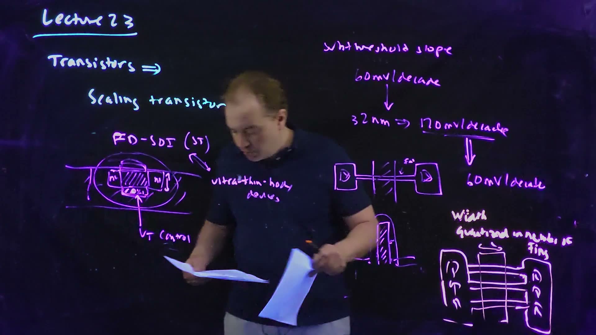
- Width in fins board. In bulk CMOS the designer changes W continuously; now “the width is effectively quantized in number of fins” (19:55).
- A three-fin device. Three fins run between shared source and drain contacts, with one gate across all of them; it has three times the drive of one fin (20:01–20:27). The layout tools (Virtuoso, at the recording) manage the fin grid.
The FinFET, redrawn from the board (Lecture23 @ 20:14). (a) From above: the fin runs from the source contact to the drain contact, and the gate crosses it; is the channel length (added). (b) Across the fin: the gate wraps the fin’s top and both sidewalls (arrows, added), over a thin gate oxide.
A three-fin device, redrawn from the board (Lecture23 @ 24:20): three fins between shared source and drain contacts, one gate across them; the curved arrow is the board’s channel-length mark. Its drive is three times one fin’s. The label is added.
How wide is a fin? added The current flows along the fin’s surfaces under the gate, so a fin’s effective width is its gated perimeter: two sidewalls of height and the top of thickness .
Derive it from the perimeter. Memorize the lecture’s part: drive is proportional to .
A fin’s width is its gated perimeter added. (a) One fin: two sidewalls of height and a top of thickness , so . (b) Fins at pitch under one gate: . For example, = 40 nm, = 10 nm and = 50 nm (illustrative, of no real process) give 90 nm per fin, and 270 nm of width in 150 nm of layout for three fins.
A worked example: width and sizing in whole fins (added; dimensions for example)
- One fin. For example, = 40 nm and = 10 nm: 90 nm of width.
- The steps. One to four fins give 90, 180, 270, 360 nm: the only widths available.
- Width without area. At a 50 nm fin pitch, three fins put 270 nm of width into 150 nm of layout, 1.8×: the fin’s height buys width without area.
- A sized path. Three inverters drive . Equal gains give 3.684 and ideal sizes 1, 3.68, 13.57 fins; the delay is 11.05 .
- Rounded to whole fins. Sizes 1, 4, 14 give gains 4.00, 3.50, 3.57 and a delay of 11.07 : +0.17 %. Large stages barely notice the rounding.
- Small devices do. A gate that wants 1.5 fins must take 1 (−33 % drive) or 2 (+33 %). Keepers and SRAM ratios, where one device must be a set fraction of another, feel the quantization most.
Check. The delay against the gains is flat near the optimum (Chapter 8), so gains of 3.5–4.0 around 3.684 should cost well under a percent; 0.17 % fits.
Traps.
- “A fin’s width is .” The current flows along the sidewalls too: the width is the gated perimeter, mostly .
- “Fins are a continuous W.” Not in a ratio that must be exact (SRAM, keepers): the nearest whole fins may be 33 % off.
- “The slope is back to exactly 60.” “Almost”: close to it, not at it.
Check yourself Why does gating a thin fin from both sides restore the slope?
The slope degrades when the gate controls only part of the barrier between source and drain, and the drain’s field controls the rest. A thin, fully depleted fin with the gate on both sidewalls (and the top) has no part of the channel far from a gate, so the gate controls the barrier almost completely and returns close to 1.
Check yourself A 6T cell in fins: the pull-down must be stronger than the access NFET for a safe read. With one fin each the ratio is 1. What is the smallest fin count for the pull-down that gives a ratio above 1, and what does it cost?
Two fins: a ratio of 2, since drive goes with the fin count; nothing between 1 and 2 exists. It costs one more fin pitch for each pull-down, so the cell grows, and the ratio is set by the fin grid rather than tuned.
Check yourself With H = 40 nm and T = 10 nm, how many fins match a planar device of 0.5 µm?
One fin is 90 nm, so fins: round up to 6 fins, 540 nm (5 fins, 450 nm, would be weaker).
7. Parasitic capacitance in 3-D devices: compact model against extraction
You need
Overlap capacitance (Chapter 5). The gate’s edge overlaps the source and drain, giving a capacitance from gate to source and from gate to drain that is there in every region of operation. In a modern device, the tall gate beside tall source/drain contacts adds more of the same kind; Lecture 5 already noted that splitting it between the device models and parasitic extraction “gets to be a little bit complicated”.
Compact models (Chapter 6). A simulator represents each transistor by a compact (SPICE) model: equations for its currents and the capacitances that belong to the device itself.
Extraction (Chapter 9). From the layout, extraction adds the resistances and capacitances of the wires and of the layout’s geometry to the netlist.
The FinFET (Section 6): the gate stands up over the fin.
The question. A FinFET is a tall, three-dimensional structure. Which capacitances surround it, which of them does the compact model include, and what does that mean for a simulation of the schematic?
Contact-to-gate capacitance (board, 20:56–23:53)
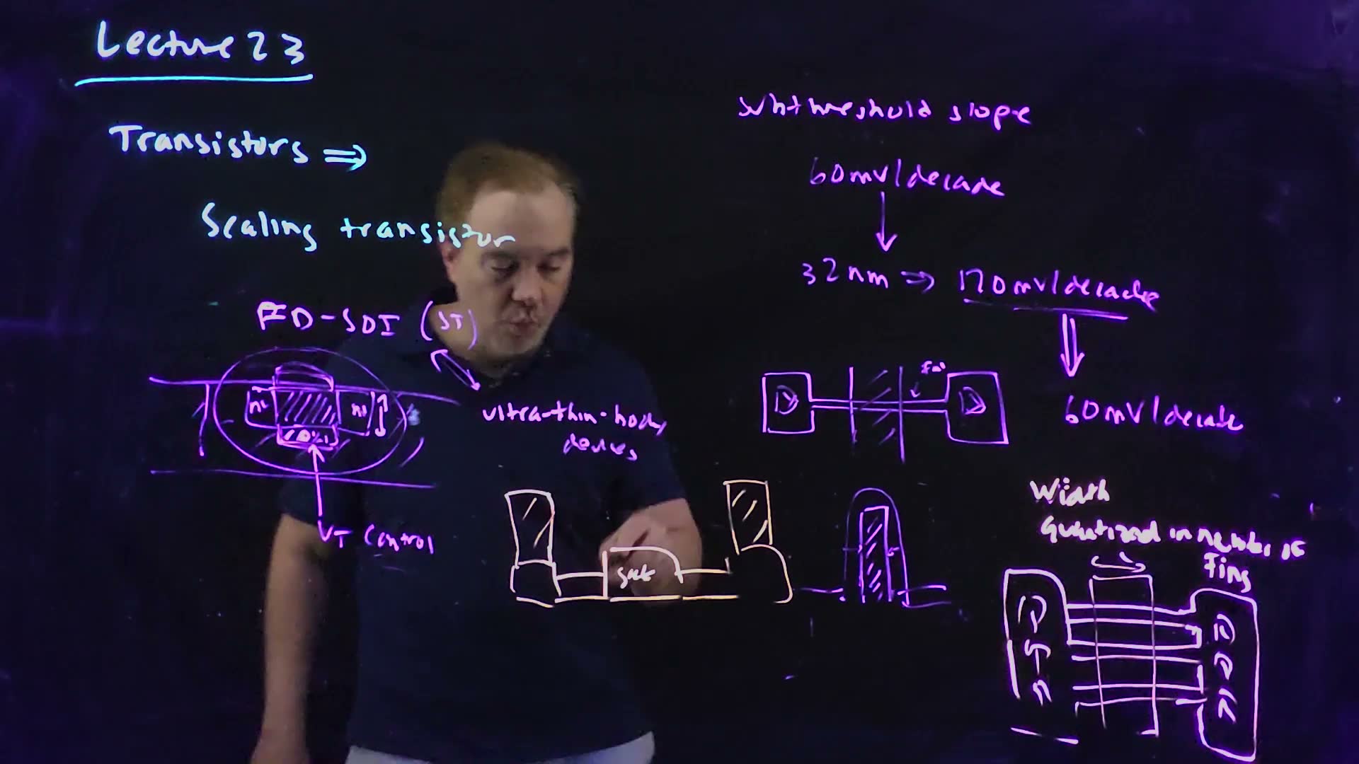
- The side view board. Along the fin: the gate stands up over it, and from the source and drain big contacts rise beside it, up to metal 1 (20:56–21:57). Between each contact and the gate there is a capacitance: the board’s two capacitor marks, later ringed.
- Two places for capacitance board. “compact model ⇒ capacitance; extraction ⇒ others” (24:20): the compact model holds some of the device’s capacitances, and extraction adds the others (22:26).
- Which is which. “These capacitances between the contact and the gate, these are not included in the compact models and are almost always included as part of extraction” (22:52). They behave like overlap capacitance: they load the gate and couple it to the drain.
- The consequence. So “your simulations with just the schematic level are not as accurate as they should be” (23:22). A schematic sees only the compact model, so it misses this capacitance and comes out optimistic. added It is the same lesson as HW4’s: extraction only adds capacitance (and resistance), so the extracted circuit is never faster than the schematic.
- Getting worse. The problem grows as devices build up “more and more in the third dimension” (23:53).
Contact-to-gate capacitance, redrawn from the board (Lecture23 @ 24:20). The contacts rise from the source and drain, beside the gate, to metal 1 (M1, added from the speech). The capacitance between each contact and the gate () is left to extraction; the gate-to-channel capacitance (, grey with dashed leads, added for contrast) is in the compact model.
Where is each capacitance? added A walk round the side view, in place of a numerical example. The lecture places only the contact-to-gate capacitance; the other rows follow the usual split.
| Capacitance | Where | Seen by |
|---|---|---|
| gate to channel () | under the gate, through its oxide, to the fin | the compact model |
| junction, fin to substrate | at the source and drain | the compact model |
| contact to gate () | across the gap between each tall contact and the gate | extraction only |
| contact to contact, contact to metal 1 | above the device | extraction |
Traps.
- “The schematic’s delay is the layout’s.” It leaves the contact-to-gate capacitance out, so the real delay is longer.
- “Add every extracted capacitance on top of the model.” Some models lump part of the parasitics in already; adding them again counts them twice. “You’ve got to be very careful to know exactly … what’s being included” (22:26).
Check yourself Why does a contact-to-gate capacitance act like an overlap capacitance?
It joins the gate to the source or drain directly, through the gap beside the gate, whatever the channel is doing: a fixed capacitance from gate to source and from gate to drain, like the overlap at the gate’s edges. On the drain side it also couples the input to the output, so a switching output doubles its effect, as Chapter 21’s Miller factor does for coupling capacitance.
Check yourself An inverter's schematic simulation gives a delay of 10 ps; extraction adds contact-to-gate capacitance on its input and output. Will the extracted delay be larger or smaller, and why can't it go the other way?
Larger. Extraction only adds capacitance (and resistance) to what the compact model already has; more charge to move through the same devices means more delay. It cannot remove the model’s capacitance, so it cannot make the circuit faster.
Check yourself Which tool step would catch a capacitance the compact model leaves out?
Parasitic extraction from the layout, followed by a simulation of the extracted netlist (Chapter 9’s flow after LVS).
8. 7 nm, 5 nm and gate-all-around nanowires
You need
The node ladder (Chapter 1). Each node’s name was of the last, so each step halved the area; after 22 nm the names became a “potpourri” that no longer measures a length. Only a few companies can still afford the leading edge (Chapter 1).
The FinFET (Section 6): a fin gated on three sides, width in whole fins.
A barrier stops carriers only if it is high and wide (Chapter 4). An off transistor’s barrier is crossed thermally (the subthreshold current); added a barrier that is thin enough is also crossed by tunnelling, as electrons tunnel through a thin gate oxide (Chapter 4 §13).
The question. Where do FinFETs end, what does a gate-all-around transistor change, and what limits scaling past it?
Past the FinFET (board, 24:12–29:12)
- Nodes without a ruler. 16, 14, 12 nm, “and continuing to go down”; the names “don’t follow the strict square root of two anymore” (24:12–24:39). added The ladder from 16 nm would give 11.3, 8.0 and 5.7 nm.
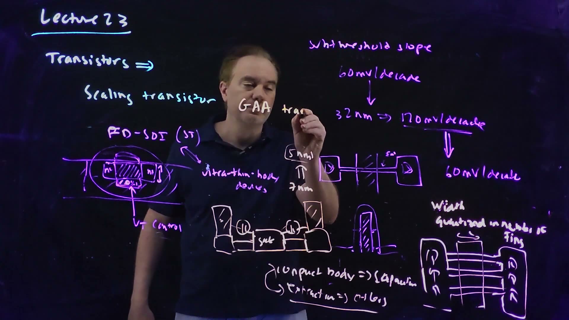
- FinFETs to 7 nm board. “7 nm ⇑ 5 nm” (25:35): the general belief at the recording was that FinFETs would reach about 7 nm (“we’re now at seven nanometers with FinFETs”).
- What stops them. At those lengths even the FinFET’s electrostatics are not enough: “the barrier heights aren’t high enough”, and carriers tunnel straight through the barrier from source to drain, direct source–drain tunnelling (24:59). Getting from 7 to 5 nm needs “even stronger barriers, even stronger electrostatics”: a gate that holds the barrier higher. added At these lengths the barrier is also very short, and a short barrier must be all the higher to stop tunnelling.
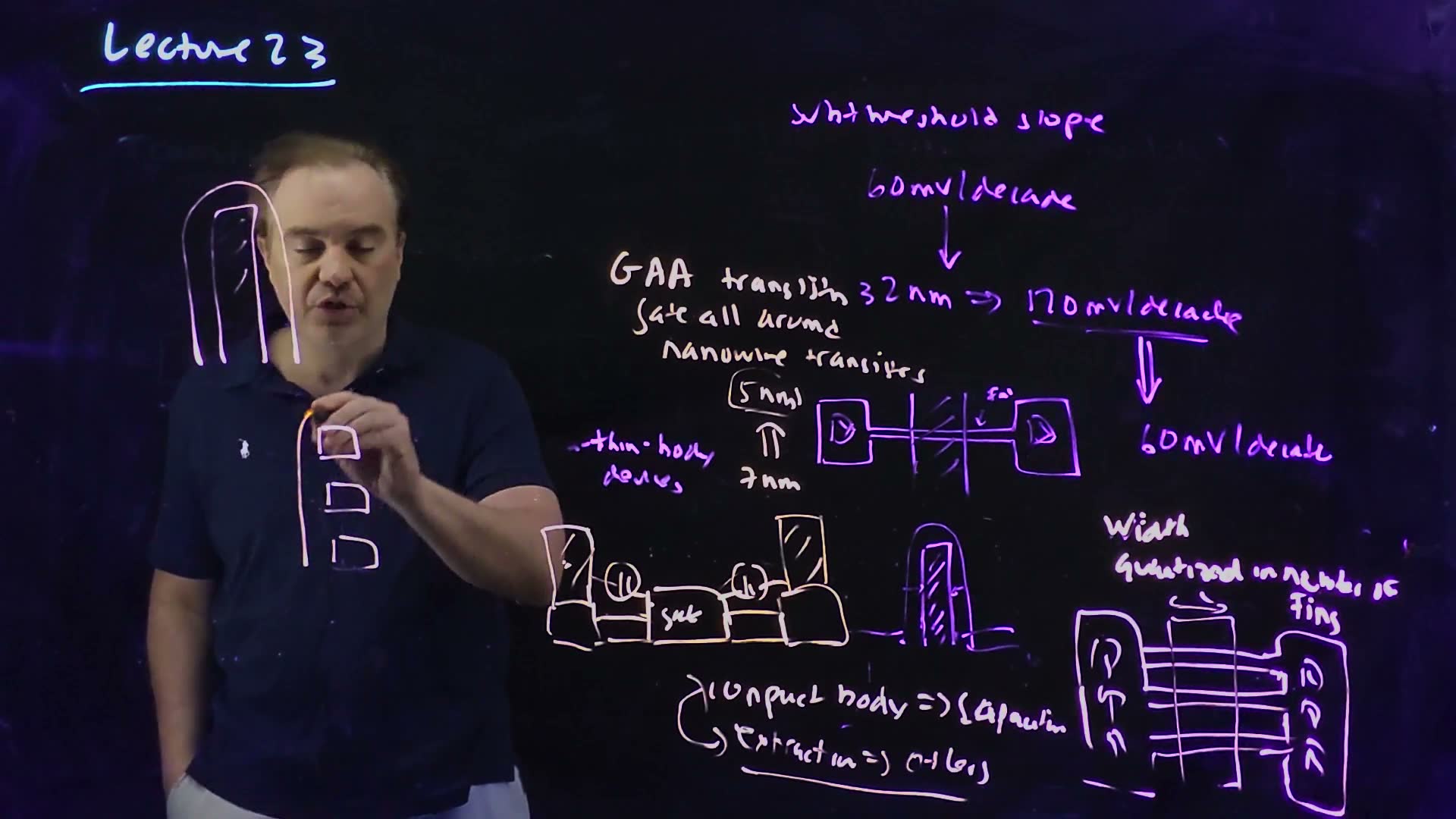
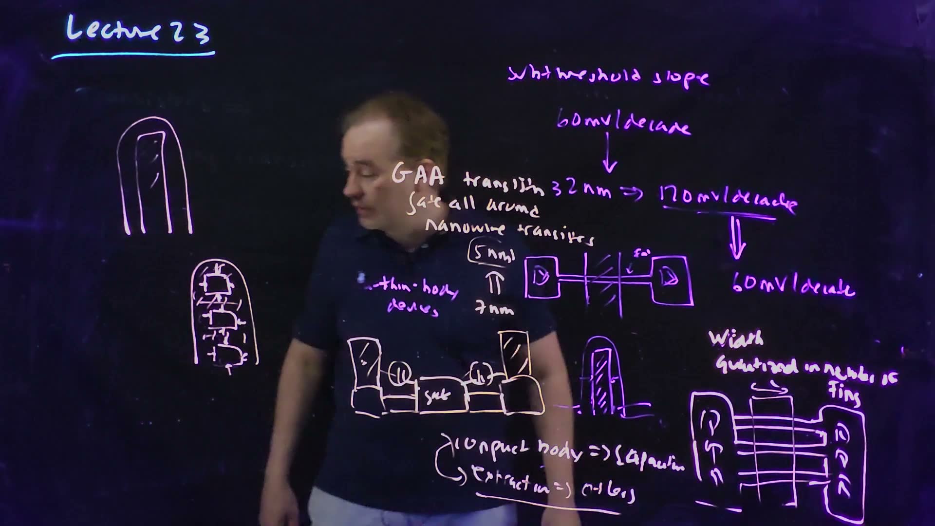
- GAA board. “GAA transistors”, “gate all around”, “nanowire transistors” (25:25–25:41). Instead of a fin’s single sheet, the channel is broken into stacked wires, three for example, each gated on all four sides; a device has a fixed number of wires per stack, and stacks are arrayed like fins (26:10–26:52).
- Who is left. Only Intel, Samsung and TSMC were still pushing the leading edge, at the recording (27:17). Chapter 1 §5’s board has the same three at about 10 nm, and only TSMC and Samsung at 5 nm.
- The end of the line? The lecturer’s view at the time: probably nothing beyond 5 nm. A well-known earlier paper had said 10 nm was the limit, and FinFETs proved it wrong; but source–drain tunnelling is a fundamental limit, “the end of the line” (27:52–28:45). Students going into industry will very likely design in FinFETs (28:45), and gate-all-around structures are “what’s going to be coming next” (29:12).
From FinFET to gate-all-around, redrawn from the board (Lecture23 @ 27:44). (a) The FinFET’s gate covers three sides of one fin. (b) A GAA (nanowire) device: three stacked wires (, added), each wholly surrounded by the gate. (c) One wire (added): its four gated faces, each of side , traced thick.
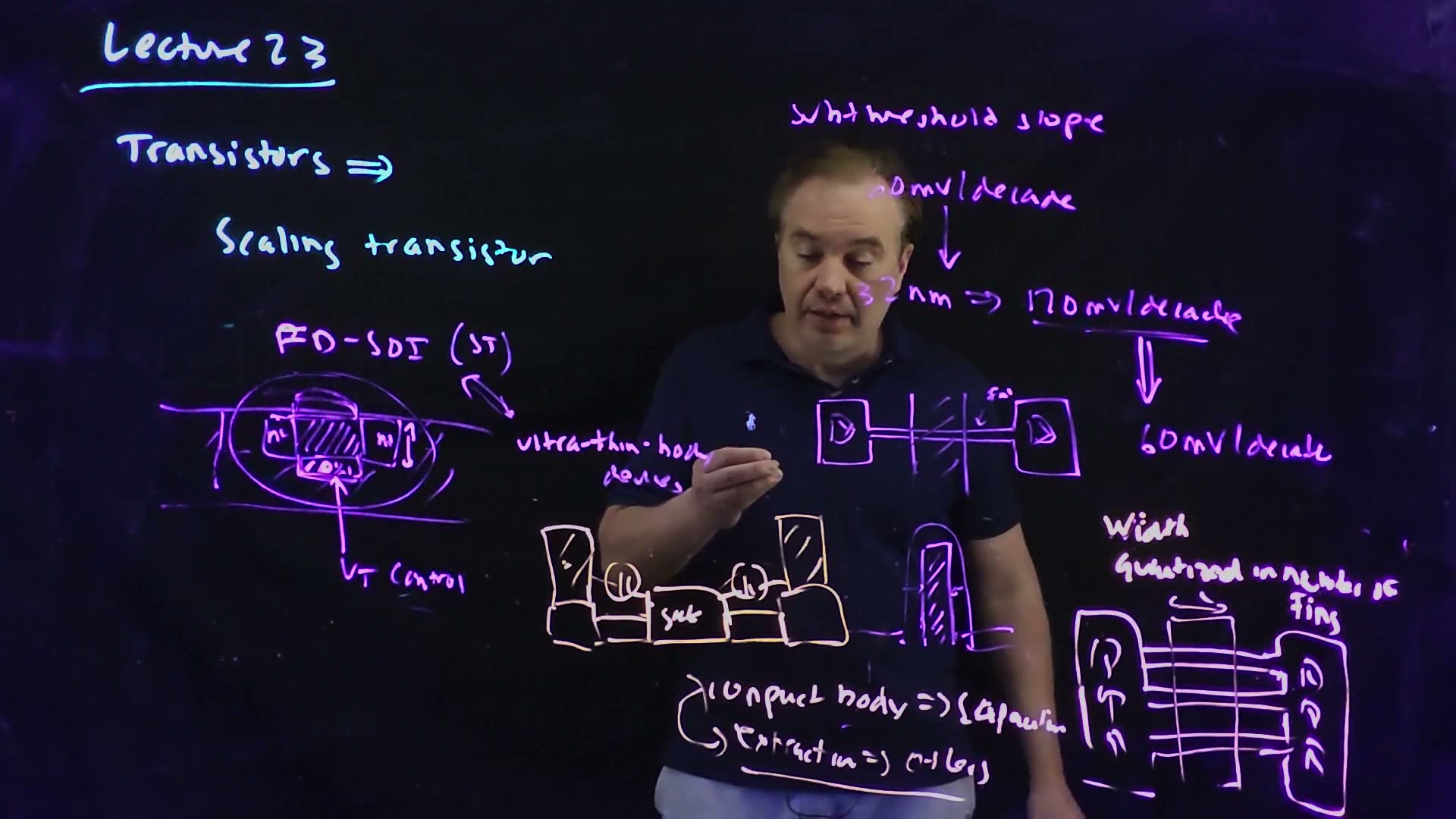
The board (Lecture23 @ 29:44)
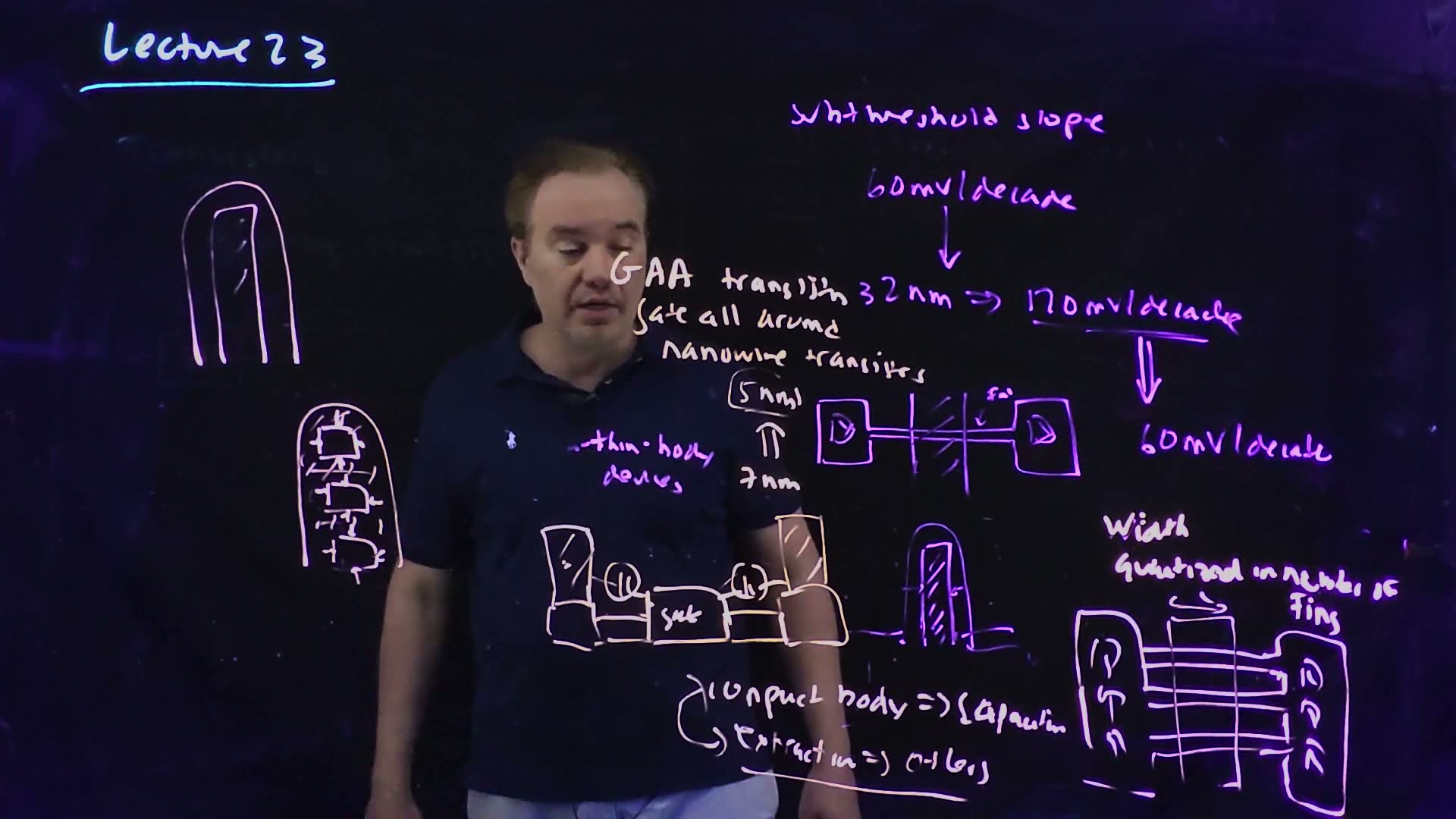
Fair copy of the board above (Lecture23 @ 29:44), mark for mark in its own layout, all in black. Three pens wrote it, each the next topic, so none takes an accent: violet the slope lines, the FinFET views and the fins; pale cream the side view with its contact capacitors, “compact model ⇒ capacitance / extraction ⇒ others” and the nanowire stack; white “GAA transistors” down to “7 nm” and the fin at the upper left. The slope is typeset 120 mV/decade, as said twice (16:58, 19:04) and as “almost a factor of two worse” than 60 requires; the hand’s middle digit, a flat top with a hooked drop, looks like its 7. The side view’s right contact, under the lecturer’s arm, is read from 28:59, where the ink is the same. “Ultra” in “-thin-body devices” is wiped; the dot before it is what remains. “transistors” after “GAA” is cramped against “32nm”, the hand’s “model” in “compact model” is cramped and reads like “body”, and “capacitance” is pressed against the fin layout: all three are set small, and “⇒ capacitance” sits a little left of its place.
How wide is a nanowire device? added As for the fin, the width is the gated perimeter, now all the way round each wire: for square wires of side , each.
Derive it from the perimeter, as for the fin.
A worked example added (dimensions for example). Three square nanowires of 10 nm side give 120 nm, against 90 nm for Section 6’s example fin. More to the point, every wire is gated on four sides, not three: no part of the channel is left for the drain to control.
Traps.
- “5 nm is the gate length.” Node names are labels now (Chapter 1 §4); nothing in a “5 nm” device need measure 5 nm.
- “GAA is new transistor physics.” It is the same MOSFET with the gate on every side. The limit it meets, tunnelling from source to drain, is the same one.
Check yourself What does a gate-all-around transistor gain over a FinFET, in one sentence about the gate?
The gate surrounds each wire on all four sides, including the bottom the FinFET’s gate leaves open, so it controls the whole channel’s barrier.
Check yourself Follow the 1/√2 ladder from 14 nm for two steps. What would the next two nodes be called, and what names did the industry use?
9.90 nm, then 7.00 nm: about 10 and 7, and the industry did call them 10 nm and 7 nm. The names happen to fit here, but by then they no longer measured any feature of the device.
Check yourself Why do carriers get through a very short channel's barrier, and what does a stronger gate do about it?
Over the barrier, carriers pass thermally, and only its height matters. Through it, they can also tunnel, and the chance falls steeply as the barrier gets higher or wider. At 7 and 5 nm the source-to-drain barrier is only a few nanometres wide, so it leaks by tunnelling unless it is high. A stronger gate (the fin’s three sides, then GAA’s four) holds the barrier higher: that is how FinFETs got below the once-predicted 10 nm limit to 7 nm, and how GAA aims at 5 nm (28:18). Past 5 nm, in the lecturer’s view, no barrier the gate can make is high enough: “you’re just not going to be able to create a barrier that the carriers can’t get through” (28:45).
On the exam
No past paper tests Lecture 23.
| Paper | Part on Lecture 23 | Sections |
|---|---|---|
| FN10, FN12, FN17, FN19; the midterms; the homework | none (a search for FinFET, SOI, floating body, soft error, gate-all-around, nanowire and fin finds no part) | — |
What this chapter gives the tested chapters:
| Number or idea | Where the exam uses it | This chapter |
|---|---|---|
| the subthreshold slope , given as 80–90 mV/decade | FN10-2, FN12-1, FN17-10, FN19-1, MT23-1b (Chapter 4 §11, Chapter 23 §15–§16) | §5: why those numbers are not 60 |
| the body effect in a stack | Chapter 5 §1 | §3 |
| the leakage step | Chapter 23 §12 | §4 |
Memorize.
- 60 mV/decade, the ideal at room temperature; about 120 at 32 nm in bulk (this lecture) and about 100 at 22 nm (Lecture 4); FinFETs near 60.
- PD-SOI: a floating body (the history effect), with less S/D capacitance and less body effect in a stack.
- FD-SOI: no body; from the work function and the film’s thickness, tuned by a back gate.
- FinFET width in whole fins; drive proportional to the fin count.
- Contact-to-gate capacitance appears only in extraction, so a schematic simulation is optimistic.
- GAA gates every wire on all sides; source–drain tunnelling is the limit past it.
Derive (with the path).
- Decades of turn-off : is linear in with slope .
- A threshold shift’s leakage change : the same line, two thresholds.
- PD or FD: compare with .
- Fin width : the gated perimeter.
Method card. None: no question family.
This was the course’s last lecture. The final-exam review pages draw on the earlier chapters; this one is context for them.
The lecture’s boards
The boards of Lecture 23 not shown above (29 frames)