F3. Past finals: path sizing
Every past final has a path-sizing question, and it is the same family as the midterms’ Question 5 (M4) and the domino sizing of MT24-5 (M6). This page re-solves the finals’ versions. They add two moves the midterms use less often: a limit on the input capacitance (FN17-7) and a limit on how far a gate may be skewed (FN19-8, FN10-9). Every number is re-solved and checked; none is copied from a key. Where a key disagrees, the folded note on the key at the end of the part explains why.
| Question | Parts | Points | Chapters | The midterm twin |
|---|---|---|---|---|
| FN17-7 (2017) | input limit, a 500 fF branch | 20 or 22 (of 250) | 8 | MT21-5 (M4 §2) |
| FN19-8 (2019) | delay, sizing within a β limit, a side branch | 35 (of 250) | 8, 11, 12 | MT24-5b–c (M6 §1), MT23-5c |
| FN12-8 (2012) | delay, sizing | 30 (of 200) | 8, 12 | solved in M6 |
| FN10-9 (2010) | delay, sizing within a β limit | 24 (of 200) | 8, 11, 12 | as FN19-8 |
FN17-7 is first because it is a purely static path, the midterms’ own problem. FN19-8, FN12-8 and FN10-9 put a dynamic gate at the head of the path. Within that family the newest exam comes first. FN19 has no answer key, so its solution here was worked out independently, and its parts have no note on a key.
Before you start
How to use this page. Each section restates one exam question with its source page (FN19-8b, p19 is the Fall 2019 final, question 8b, physical PDF page 19) and its points, and shows the exam’s own figure. FN17-7 is the static path-sizing family that M4’s approach section teaches; its parts say what this question adds. The path with a dynamic first stage is taught in full here, in the How to approach section before Section 2. Every part is worked the same way: what it asks, the idea behind the method, the solution in steps (each step gives its reason first), a check on the result, the answer, and one thing to remember. Try each part on your own first; open the Hint if you are stuck, and step through the solution before you press “Show all”.
The methods are all in the chapters:
- a gate’s gain from its normalized inverter (Chapter 8 §1), and the stack rule (Chapter 7 §8);
- path delay and path effort (Chapter 8 §2); equal gains , sized back from the load (§3, §6);
- branching and retuning around a side load (§8, §9);
- the logical effort of a dynamic stage, counted on the one edge it makes, footer included (Chapter 12 §1, §2);
- skewed inverters and skewed static gates (Chapter 12 §4).
The conventions of each exam. Only gate capacitance counts (each exam says so or gives no other). Loads are written as microns of gate, .
| Exam | Device strengths | Loads in µm of gate | ||
|---|---|---|---|---|
| FN17-7 | 100 ps (given) | 2 fF/µm | “the nFET has twice the on current of the pFET”: | : 100 fF = 50 µm; : 500 fF = 250 µm; input limit 2 fF = 1 µm |
| FN19-8 | 25 ps (the given FO1 delay) | 1 fF/µm | not stated; assumed (see §2) | : 700 fF = 700 µm; side branch 200 fF = 200 µm |
| FN10-9 | ps | 2 fF/µm | , | : 700 fF = 350 µm |
With the balanced inverter is 2W/W with input ; , , . The FO1 delay of that inverter is (Chapter 7 §7).
1. FN17-7: an input limit and a 500 fF branch
The question (FN17-7, p17). The fan-out-of-one delay is ps and the gate capacitance is 2 fF/µm. “As always, assume that the nFET has twice the on current of the pFET at the same channel width.” The path runs from A through stage I (an OAI gate on A, B, C, D), stage II (a NOR), stage III (an inverter) and stage IV (a NAND) to Y, which drives 100 fF. A capacitor hangs on the NOR’s output.
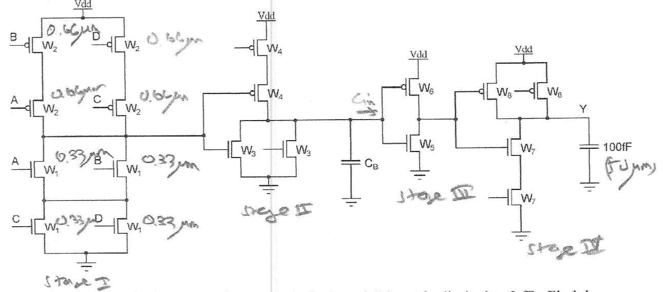
Reading the circuit
Every part needs two numbers for each gate: the capacitance of one of its inputs (the load it puts on the stage before it) and its logical effort . No width is given, so you also balance each gate yourself, and that ties its two widths together. The strengths are unequal: “the nFET has twice the on current of the pFET” means , so a PFET must be twice as wide as an NFET to pull as hard, and the balanced inverter is 2W/W, with input .
Reading FN17-7 gate by gate
- Stage I, the OAI22, . When one input switches, the output falls through two NFETs in series ( each: A or B, then C or D) and rises through two PFETs in series ( each). Two equal devices in series act like one of half the width, so the gate is balanced when its PFETs are twice its NFETs, . It then drives like a over inverter, whose input is . One input drives one NFET and one PFET, , so .
- Stage II, the NOR2. One NFET () pulls down alone, because in the worst case only one input switches. The two PFETs () are in series and act like , which must be twice to balance: . The normalized inverter is over , input ; one input drives , so .
- Stage III, the inverter. Because , its PFET must be twice as wide as its NFET to pull as hard, so it is balanced at : input , .
- Stage IV, the NAND2. The two NFETs () in series act like ; one PFET () pulls up alone and must be twice that, so . The normalized inverter’s input is ; one input drives , so .
- The loads, in µm of gate, because every gain is a ratio of gate widths. At 2 fF/µm, Y’s 100 fF is 50 µm, the 2 fF input limit is 1 µm, and fF is 250 µm. hangs on the wire from the NOR’s output to the inverter’s input: the load of stage II.
| Stage | Gate | Balanced widths () | One input | |
|---|---|---|---|---|
| I | OAI22, | stacks of two both ways: NFETs act as , PFETs as ; balanced when | ||
| II | NOR2 | NFETs alone (worst case); PFETs in series act as , so | 5/3 | |
| III | inverter | 1 | ||
| IV | NAND2 | NFETs in series act as ; one PFET | 4/3 |
The edges. Every gate inverts, so the edges alternate. With C or D at 1, B at 0, the NOR’s other input at 0 and the NAND’s other input at 1: A rises, the OAI output falls, the NOR output rises, the inverter output falls, and Y rises. “A falling to Y falling” is the mirror case; every gate is balanced, so its gains are the same and one sum serves both. This is MT21-5’s circuit, with in place of equal strengths (M4 §2).
FN17-7a: the input limit (8 or 10 points)
FN17-7a, p17. Let , and let the input capacitance of each of A, B, C and D be limited to 2 fF. Find the sizing that gives minimum delay from A rising to Y rising (or A falling to Y falling). (The point value is overwritten in the source: 8 or 10.)
Hint
What it asks. Choose all eight widths for the fastest path from A to Y, with no branch yet (), when each input may present at most 2 fF. The words “limited to 2 fF” take the place of a fixed first gate: they are what stops you making every gate huge and pushing the delay onto whatever drives A.
The idea. This is MT21-5a, which M4 works in full, with the moves of M4’s path-sizing section. The new point is the strength convention. With every PFET doubles, so the NOR’s is and the NAND’s , where MT21-5 has for both, and against MT21-5’s 4.5. The rest is the same. With nothing branching off the path, the product of the four gains is the path effort (Chapter 8, Section 2):
is the cost of the gate types and the load over the path’s input capacitance; doesn’t depend on the inner widths, because each one is the load of one stage and the size of the next, and cancels. A sum of factors with a fixed product is smallest when the factors are equal: making one stage faster forces another to be slower by a larger factor. So every stage takes (Chapter 8, Section 3).
FN17-7a
- Use the whole input limit. falls as the input grows, so a larger input means a smaller and a faster path. Take A’s input at 2 fF = 1 µm: with , which gives m and m.
- The path effort, because it sets the stage gain: , and .
- Equal gains. Four stages share it equally: .
- Size back from the load (Chapter 8 §6), because the load is the one capacitance known at the end. Write each gain as , with the stage’s one-input capacitance. NAND: gives m, so m.
- Inverter. It drives the NAND’s input: gives m, so m and m.
- NOR. It drives the inverter’s input: gives m, so m and m.
- Stage I checks the work. Its gain isn’t chosen, but the four gains multiply to , so it must come out at : . ✓
- The delay. Four stages at each: ns.
Check. Use only half the limit, 1 fF: and double, to 444.4, and the delay becomes , 19% slower. The delay grows as , so the whole limit is worth taking, and it is the only thing that sets the first gate’s size.
Answer: , , , , , , m; delay ns. Using the whole input limit is the same step as MT21-5a.
Remember. A cap on the input makes smallest when you use all of it; then size back from the load. When the strength convention changes, rework every first: the method is MT21-5’s, the numbers are not.
The answer key agrees
It gives the same sizes ( from its rounded 4.5 µm), and no delay.
FN17-7b: a 500 fF branch (12 points)
FN17-7b, p18. Now fF. Find a sizing that gives you close to the minimum delay for this path from A rising to Y rising (or A falling to Y falling).
Hint
What it asks. Hang 500 fF on the NOR’s output and resize for a delay close to the minimum. A’s input stays at the 2 fF limit, so and stay. “Close to the minimum” means that a sensible retuning, explained, is enough.
The idea. This is MT21-5b’s dominant branch (M4), with this exam’s gains. The branch is 250 µm of gate. It doesn’t grow when the gates after it grow, so the path effort is no longer fixed (Chapter 8 §8), and is no longer the answer. But equal gains still hold on any piece of the path with nothing branching off it. Retune by inspection, as the lecture does (Chapter 8 §9), in two moves:
- Rebalance first. The branch is 98% of the NOR’s load, so at (a)‘s sizes the NOR’s gain jumps to 219.7 while the OAI’s stays at 3.86. The lecture’s example enlarges the gate after the branch first, but its branch driver was already sized for the branch. Here, enlarging the inverter first (to a 17.5 µm input) would add to that huge gain, and the delay would rise from to .
- Then enlarge the gate after the branch: here it pays. Split the path at the branch added. Because the branch dominates, a larger inverter adds little to the NOR’s load and makes the last two stages much cheaper. The best size is where those two changes match.
FN17-7b
- See what the branch does at (a)‘s sizes. A side load adds only to the stage that drives its node, so only the NOR’s gain changes. It now drives m from its 1.93 µm input: gain . Delay ns.
- Rebalance the pair before the branch. A’s input is fixed and nothing branches between the OAI and the NOR, so while only the NOR moves, the product of their two gains stays at . Equal factors give the smallest sum: each. The NOR’s input becomes m (, m).
- The delay now: ns, already a factor of 3.5 better.
- Split the path at the branch, because each side then has nothing branching off it. Call the inverter’s input (µm), as the key does. Stages I and II share the product ; stages III and IV share .
- The delay for a chosen . A balanced pair with product contributes , so the delay is (in ).
- Try a few widths. Growing raises the first term slowly and lowers the second fast, until the two changes match. : 65.97. : 64.04. : 63.63. : 64.08. Take m.
- Stages III and IV, balanced: each. The NAND’s input is m, so m. The inverter: , m.
- Stages I and II, balanced: each. The NOR’s input is m, so and m. and stay at 0.33 and 0.67 µm.
- The delay: ns.
The exact minimum added. Setting the derivative of step 5’s expression to zero gives , that is , whose real root is m. That is the key’s method. It is added calculus: the lecture says the retuning can be done exactly, but usually “you just sort of look at it” (L08 52:20–53:19). Trying three or four widths, as in step 6, finds the same minimum to within 0.01%.
Check. A floor. Whatever the sizes, the pair before the branch must carry a product of at least , so it costs at least . No sizing reaches that, because the stages after the branch would have to cost nothing; 63.63 is about 10% above it.
Answer: , , , , m (with , as in (a)); delay ns. Step 2 alone (6.60 ns) is already close to the minimum. Most of what remains is the cost of driving 250 µm from a 1 µm input, which no sizing removes.
Remember. With a heavy branch, first share the overloaded stage’s gain with the stage before it; then enlarge the gate after the branch. The larger the branch’s share of the load, the more the first move does and the more the second one buys.
The answer key differs
It says that at (a)‘s sizes stage II’s gain is 212 and the delay . The gain is 219.7 and the delay (the key’s 212 is read from the transcription; the page scan is not in the sources). After that its minimization is right: m, gains 29.9 and 1.95, , , , , m and (63.6 unrounded). Two slips in its working don’t change the result: one line writes where the lines around it have , and the line’s denominator reads , where its own 5.8 µm needs 1.95.
The widget below does steps 4–6 for any inverter size. Slide the input of the inverter after the branch; the red point is (a)‘s sizing with the branch added, and the green point the lowest delay.
How to approach a path with a dynamic first stage
Recognize it by a clocked gate at the head of a path: a PFET on from to a node, an NFET network below it over a footer on , then an inverter and static NANDs (or a second dynamic stage), every width labelled , and a large capacitor at the end. The phrases: “in the evaluate phase ()”, “keeping fixed”, “do not let the beta ratio … become more than 4 or less than 0.25”, and sometimes a side branch. Three finals asked it: FN19-8 for 35 points (of 250), FN12-8 for 30 and FN10-9 for 24 (of 200). The parts come in a static path’s order (M4’s path-sizing section): the delay as drawn, then the sizes for the least delay, then a side load at fixed sizes.
The moves, in order.
- Mark the edges in evaluate. The precharged node can only fall, and every stage after it inverts, so the edges alternate: X falls, C rises, D falls, E rises. Check that the edge pair the question names is one the path can make.
- Take each stage’s on its own edge. For the dynamic stage, count every device from the node to ground, footer included, and ignore the precharge PFET: it is off during evaluate (M6’s dynamic-logic section). For a static gate, only the network that makes its edge counts.
- State the strength convention, because it sets and every . FN10 and FN12 give ; FN19 doesn’t, so write down the one you use and why.
- Skew each static gate toward its edge, to the limit. Each makes only one edge in evaluate; its other network only resets the node in precharge. Shrink that network until the β limit stops you: the input gets smaller while the edge that matters keeps its strength, so falls.
- Size for equal gains. With fixed and nothing branching off, is fixed: take , size back from the load, and let stage I come out at as a check (M4’s path-sizing section).
- A side branch at fixed sizes changes one gain: that of the stage that drives its node.
Why these formulas.
- Gain and path delay. In the course’s model, with gate capacitance only, each stage takes times its gain . Here is the gate it drives over its own input, and its input over the input of the balanced inverter that pulls as hard on the same edge. The path delay is (Chapter 8, Section 2). A static gate’s input drives an NFET and a PFET; that is the cost measures.
- The dynamic stage. Its input drives one NFET and no PFET. Its evaluate path is the input and the footer in series: two 1 µm devices act as one of 0.5 µm. With the balanced inverter with that pull-down is 1 µm over 0.5 µm, input 1.5 µm, so , the lecture’s board value (Chapter 12, Section 2). In general added a -high stack of equal devices has with and at equal strengths (the general rule).
- A skewed gate added. The same definition, on the edge that matters: its input over the balanced inverter with the same strength on that edge (Chapter 12, Section 4). A NAND2 with NFETs and PFETs , falling: the stack acts as , the balanced inverter’s input is , the NAND’s own input , so instead of .
- The β ratio compares strengths, not widths. With a PFET is as strong as an NFET of half its width. So the inverter is at , and a NAND2 with PFETs over two series NFETs is at .
Decisions to make on the way. The strength convention, with a reason when the exam leaves it out. Which edge each static gate makes, and so which way to skew it. Which node a side load hangs on.
Traps. An edge pair the path can’t make (a dynamic node never rises in evaluate). Leaving out the footer, or counting the precharge PFET. Reading β as a width ratio, which puts the 8:1 inverter over the limit. Skewing a gate toward the edge it doesn’t make. The units of a load: 700 fF is 700 µm at 1 fF/µm but 350 µm at 2 fF/µm. Treating as fixed after a side load is added.
2. FN19-8: a dynamic gate, a skewed inverter and two NANDs
The question (FN19-8, p18). A path from a dynamic gate through, in the exam’s words, “two static gates”; the figure has three, a skewed inverter and two NAND2s. The gate capacitance is 1 fF/µm, and the FO1 delay of the technology is ps. Node E drives 700 fF, and a capacitor hangs on node D.
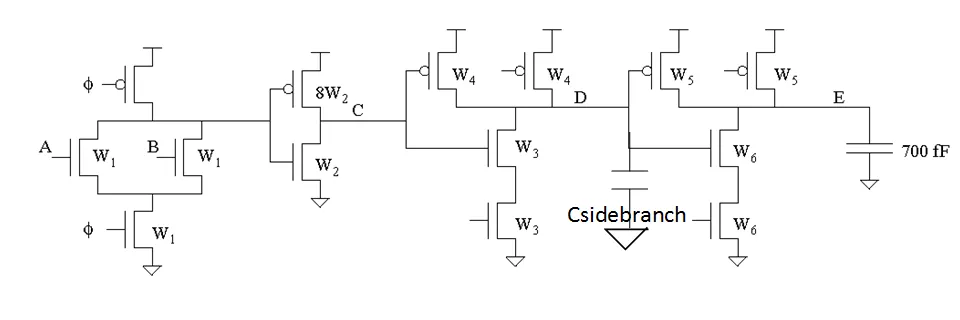
Reading the circuit
Every part needs each stage’s edge and its on that edge, so find them once, in the order of the moves above. Start with the strengths, because every depends on them.
The strength convention. FN19 doesn’t say how strong a PFET is. Take , the course’s usual convention and the one FN10-9 states for this same circuit. Two things in the problem support it. The given inverter’s strength ratio is then , exactly the limit part (b) sets. And the given FO1 delay is then ps. With equal strengths the 8:1 inverter would already break (b)‘s limit.
Reading FN19-8 stage by stage
- The inputs that hold the path open. B is at 0, so A’s NFET alone pulls X down; each NAND’s other input (drawn as a stub) is at 1, so each NAND passes the path’s signal on, inverted.
- The edges, because each stage’s is taken on its edge. In evaluate () the precharged node can only fall, so A rising makes X fall. Each later stage inverts: C rises, D falls, E rises. These are exactly the edges the question asks about: “A rising to E rising” is an edge pair this path makes (Chapter 12 §1).
- Stage I, the footed dynamic OR. X falls through A’s NFET and the footer in series, two devices that act as one of . The balanced inverter with that pull-down has a PFET, input . A drives one NFET and no PFET, : (Chapter 12 §2). The precharge PFET is off during evaluate and plays no part (its width isn’t even given).
- Stage II, the inverter , rising. Only its PFET makes C rise. The balanced inverter with an PFET has a NFET, input ; the real input is : added.
- Stage III, a NAND2, falling. D falls through the two NFETs in series, which act as ; the balanced inverter with that pull-down has input . One input drives one NFET and one PFET, . At 1 µm, .
- Stage IV, a NAND2, rising. E rises through one PFET, as strong as a NFET; the balanced inverter has input . One input drives . At 1 µm, .
- The loads, in µm of gate, because every gain is a ratio of gate widths: at 1 fF/µm, E’s 700 fF is 700 µm, and the side branch’s 200 fF is 200 µm, on D.
| Stage | Gate | Edge | What pulls it | Balanced inverter with that strength | Input | (all 1 µm) |
|---|---|---|---|---|---|---|
| I | dynamic OR, footed | X falls | A’s NFET over the footer: like one | NFET , PFET : | 2/3 | |
| II | inverter | C rises | the PFET | PFET , NFET : | 3/4 | |
| III | NAND2 (PFETs , NFETs ) | D falls | two in series: | 4/3 | ||
| IV | NAND2 (PFETs , NFETs ) | E rises | one | 4/3 |
FN19-8a: the delay as drawn (10 points)
FN19-8a, p18. Estimate the delay from A rising to E rising in the evaluate phase () if m. Let .
Hint
What it asks. The delay from A rising to E rising in evaluate, with every width at 1 µm and no side branch, in units of the 25 ps FO1 delay and then in ns. Nothing is sized yet: this is the path as drawn.
The idea. Each stage takes times its gain , with from the table, on the stage’s own edge, and the gate it drives over its own input. The stages switch one after another, so the delays add (Chapter 8, Section 2). What is new against a static path is only the s: a dynamic input that carries no PFET (2/3), and gates whose edge the clock fixes, so only the network that makes that edge counts. The tempting slip is to give the 8:1 inverter a balanced inverter’s , or its falling edge’s 3: only C rising is on the path.
FN19-8a
- Stage I. X drives the whole input of the inverter, both of its gates, m, from A’s 1 µm: , gain .
- Stage II. C drives one NAND input, its NFET and its PFET, m, from 9 µm: gain . A large gate driving a small one is fast, but its size is wasted.
- Stage III. D drives the next NAND’s 2 µm from 2 µm: gain .
- Stage IV. E drives the 700 µm load from 2 µm: gain .
- Add the gains. Delay ns.
Check. The big term by : the one 1 µm PFET has resistance and drives 700 fF, and over is . ✓ The two routes agree, because logical effort is the same model in other units.
Answer: ns. The last NAND, driving 700 fF through one 1 µm PFET, is 98% of it.
Remember. Mark the edges, then take each on its own edge: a dynamic input carries no PFET, and a skewed inverter counts only its strong device. The rest is a static path’s sum of gains.
FN19-8b: sizing within the β limit (15 points)
FN19-8b, p19. Keeping fixed at 1 µm, resize the network to minimize the delay from A rising to E rising with . Do not let the beta ratio (the ratio of pFET strength to nFET strength) of any gate become more than 4 or less than 0.25.
Hint
What it asks. Choose to for the least delay from A rising to E rising, with no side branch, while every gate’s β (PFET strength over NFET strength) stays between 1/4 and 4. Two phrases decide the method. “Keeping fixed” fixes the path’s input, so the path effort is fixed. The β limit allows the gates to be skewed, and says how far.
The idea. Two moves, in this order.
- Lower by skewing. Each static gate after the dynamic stage makes only one edge during evaluate; the network that makes the other edge only resets the node during precharge (Chapter 12 §4; L12 06:58 and 09:02). Shrinking that network lowers the gate’s input capacitance and leaves the edge that matters as strong as before, so its on that edge falls. Nothing in the model pays for it added: the model counts only gate capacitance, and the reset edge isn’t timed. So go to the limit.
- Then size for equal gains. With fixed and nothing branching off, doesn’t depend on the widths, and a sum with a fixed product is smallest when its factors are equal: every stage takes , and no stage can be made faster without slowing another by more (Chapter 8 §3).
FN19-8b
- Read each gate’s β, because the limit is on strength, not width. With a PFET is as strong as an NFET of half its width. Stage II: , already at the limit, so it stays 8:1. Stage III: PFET against the NFET stack’s , so . Stage IV: .
- Skew III toward its NFETs, because D falls: the smallest allowed is 1/4, so . Its input is against the balanced inverter’s : , down from 4/3.
- Skew IV toward its PFETs, because E rises: the largest allowed is 4, so . Again .
- The path effort, because it sets the stage gain. With fixed, A’s input is 1 µm and the load 700 µm: . , and . Nothing branches off and every gate keeps its proportions, so doesn’t depend on the widths and equal gains are the minimum.
- Equal gains: .
- Size back from the load, because its equation has only one unknown. IV: gives m and m (D drives m).
- III drives that 147.7 µm: gives m and m (C drives m).
- II drives that 31.2 µm: gives m: the PFET is m and the NFET 0.658 µm.
- Stage I checks the work. Its gain isn’t chosen, but the four gains multiply to : . ✓
- The delay. Four stages at : ps.
Check. The last stage by : the 118.2 µm PFET has resistance and drives 700 fF, which in units of is , the same . ✓
Answer: (PFET 5.26), , , , m; delay ps, down from 11.9 ns. Without the skew (NANDs at ), and the best is ps: the β limit is worth about a fifth of the delay.
Remember. After a dynamic stage, skew every static gate toward the edge it makes, to the β limit. Then the path is a static one with a smaller : equal gains, sized back from the load.
FN19-8c: the side branch (10 points)
FN19-8c, p20. Using the sizing of (b), what is the delay from A rising to E rising with fF?
Hint
What it asks. Keep the sizes of (b), hang 200 fF on D, and find the new delay. No retuning is asked.
The idea. A side load is extra capacitance on one node, and each node is driven by exactly one stage. So it raises that one stage’s load, and with it that stage’s gain. Every other stage drives what it drove before, at the same size, so its gain doesn’t change. This is MT23-5c’s move (M4); here the node is D, the output of the skewed NAND III.
FN19-8c
- Find the node, because it names the one stage that changes. The capacitor hangs on D, the output of stage III. At 1 fF/µm it is 200 µm.
- Add it to stage III’s load. Stage III now drives m from the same pull-down, whose balanced inverter’s input is m: gain , up from 3.95.
- The other three gains stay at 3.948, because their loads and their sizes haven’t changed.
- The delay: ps.
Check. The delay rose by , exactly the rise in stage III’s gain, from 3.95 to 9.29: nothing else moved.
Answer: ps. The branching factor at D is . The question doesn’t ask for retuning. If it did, the moves of FN17-7b would apply. Resizing all three free widths reaches ps, with the last NAND larger (m): try it in the widget of Section 5.
Remember. At fixed sizes, a side load changes one gain: that of the stage driving its node. Find the node first.
3. FN12-8: a domino path (solved in M6)
FN12-8 (Fall 2012 final, p12–13, 30 points) asks for the evaluation delay from A to G of a domino path (a footed dynamic OR, a inverter, a three-high dynamic stage and a inverter driving 500 fF, with , and 2 fF/µm) with all widths 1 µm, and for the sizes that minimize it with fixed. M6 §4 solves it in full, as an extra drill.
Answer: (a) ns; (b) , , , , m, about 315 ps.
The answer key differs
It adds its gains to 50.76 and multiplies them to 128.94; its method is right.
4. FN10-9: the same path in 2010
The question (FN10-9, p15). The same circuit as FN19-8, with no side branch. The gate capacitance is 2 fF/µm; the unit-width nFET resistance is 4 kΩ and the pFET’s 8 kΩ (that is, kΩ·µm). Ignore diffusion and overlap capacitance. E drives 700 fF.
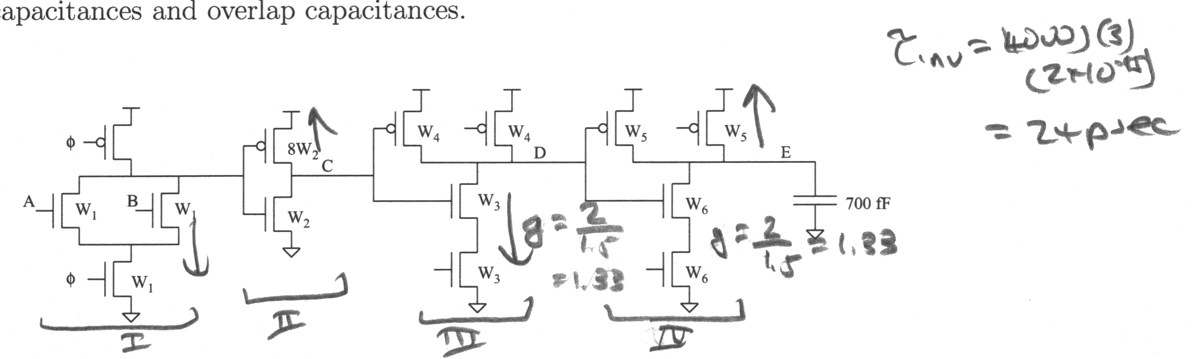
ps, because the FO1 delay of the 2W/W inverter is its NFET’s driving its own of gate. The load is m, because gains are ratios of gate widths. Here is given, so nothing is assumed, and the edges and the logical efforts are those of the table in Section 2: X falls, C rises, D falls, E rises.
FN10-9a: the delay as drawn (10 points)
FN10-9a, p15. Estimate the delay from A rising to E rising in the evaluate phase () if m.
Hint
What it asks. The delay from A rising to E rising in evaluate, with every width at 1 µm, in ns. It is FN19-8a in other units.
The idea. Same path and the same moves as FN19-8a: each stage takes times its gain , with on its own edge, and the gains add. What is different is the units. The strengths are given (, so nothing is assumed), is not given but follows from ps, and at 2 fF/µm the 700 fF load is only 350 µm of gate, half of FN19-8’s.
FN10-9a
- Stage IV. E drives the 350 µm load from one NAND input, 2 µm, with on its rising edge: .
- Stage III. D drives the next NAND’s 2 µm from 2 µm: .
- Stage II. C drives 2 µm from the inverter’s 9 µm, with on its rising edge: .
- Stage I. X drives the inverter’s 9 µm from A’s 1 µm, with : .
- Add the gains. Delay ns.
Check. Both ends by . Stage IV: one 1 µm PFET is 8 kΩ, and ns ps. ✓ Stage I: the two 1 µm NFETs in series are 8 kΩ, driving 9 µm × 2 fF/µm = 18 fF: ps ps. ✓
Answer: ns.
Remember. Before anything else, convert the load to µm of gate at the exam’s , and find from : the same circuit at 2 fF/µm has half the load in µm, and half the last stage’s gain.
The answer key agrees
FN10-9b: sizing within the β limit (14 points)
FN10-9b, p16. Keeping fixed at 1 µm, resize the network to minimize the delay from A rising to E rising. Do not let the beta ratio of any gate become more than 4 or less than 0.25.
Hint
What it asks. As FN19-8b: with fixed and every gate’s β between 1/4 and 4, choose to for the least delay from A rising to E rising. There is no side branch.
The idea. FN19-8b’s two moves (Section 2): skew each NAND to its β limit toward the edge it makes, which lowers , then take equal gains with the fixed : the product of the gains is fixed, so their sum is smallest when they are equal. What is different is only : the load is 350 µm of gate instead of 700. The gates and the skew are the same, so is the same 0.347, halves, and each stage’s gain is smaller.
FN10-9b
- Skew to the limits, because each NAND makes only one edge in evaluate: (III falls) and (IV rises), so stages III and IV have . Stage II is already at .
- The path effort, because it sets the stage gain: ; .
- Size back from the load, because its equation has only one unknown. IV: gives m and m (D drives 87.8 µm).
- III drives that 87.8 µm: gives m and m (C drives 22.0 µm).
- II drives that 22.0 µm: gives m (PFET 4.43 µm).
- Stage I checks the work: . ✓
- The delay. Four stages at : ps.
Check. Against FN19-8b: only halved, so halved, and each of the four gains is divided by : . ✓
Answer: , , , , m; delay ps, down from 5.78 ns. Unskewed, the best would be ps.
Remember. With the same gates and the same skew, only moves the result, and the best delay grows only as .
The answer key differs
It skews the same way (), gets and the same widths. Its is cut short. It gives no delay for the resized path: 319 ps. Its fourth root multiplies (a)‘s rounded gains, which give 122 rather than 121.5; the root is 3.32 either way.
5. Resize it yourself
The widget holds FN19-8 and FN10-9 as written above, with , and on sliders; and follow from the reading you choose. “Balanced NANDs” keeps and , so it opens at part (a), every width 1 µm. “Skewed to the β limits” is part (b): , ; press “sizes of (b)” or “lowest delay”. For FN19-8, “skewed, 200 fF on D” with the sizes of (b) is part (c).
What to notice.
- With no side load, stays the same whatever you do with the sliders, and the lowest delay has four equal gains (FN19-8: 3.948 each).
- Switching between “balanced” and “skewed” changes only : the best delay drops from 499 to 395 ps (FN19-8) and from 403 to 319 ps (FN10-9).
- With 200 fF on D, moves as you resize, because the fixed 200 µm sits beside NAND IV’s input in stage III’s load. Equal gains are no longer the best. The lowest point (486 ps) has a larger than (b): the “enlarge the gate after the branch” move.
What this means for the midterm
Which midterm family uses each method.
- FN17-7 is the static path family of M4: the input limit is MT21-5a, and the dominant branch is MT21-5b, where rebalancing the pair before the branch does most of the work. MT23-5 and MT17-5 have the smaller branches, where enlarging the gate after the branch first can even hurt.
- FN19-8 and FN10-9 join a dynamic stage to the static method; the approach section has the moves and why they work. The dynamic logical effort ( for an n-type stack with , at equal strengths) is MT23-3b’s and MT24-5b’s (M6); equal-gain sizing with the first gate fixed is MT23-5b and MT17-5b; the side branch at fixed sizes is MT23-5c and MT17-5c. A strength-ratio limit has not appeared on a midterm, but MT23-3c’s skewed inverter is the same idea.
- FN12-8 is the domino-sizing drill already in M6.
Traps (the approach section explains each).
- State the edges first, and check that the named edge pair can happen (MT24-5b’s key and FN17-2c’s ask for edges that can’t).
- Count the footer in the dynamic stack; ignore the precharge device.
- Use the whole input limit (FN17-7a, MT21-5a): a bigger first gate always helps.
- Skew toward the edge that matters, to the limit; β compares strengths, not widths.
- A side load changes one gain only at fixed sizes: the stage that drives that node.
- Read the units. A 700 fF load is 700 µm at 1 fF/µm but 350 µm at 2 fF/µm.
Time. On these finals a point was worth about 43 seconds (180 minutes for 250 points), so FN19-8 had about 25 minutes and FN17-7 about 15. On a midterm pace (22.5–30 seconds a point), an (a) part takes 3–4 minutes, a (b) sizing 6–8, and a retuning around a branch 8–10. Write the gains in a table first; the arithmetic then takes little time.