M4. Past midterms: path sizing
Question 5 of three of the four past midterms is the same kind of problem. You get a path of four static CMOS gates driving a large load, with every width given, and you estimate its delay. Then you size the path for minimum delay with the first gate fixed. Then a side load is added in the middle, and you retune around it. It is worth 40, 35 and 40 of 150 points (MT23, MT21, MT17), about a quarter of each exam. MT24 moved the sizing into a dynamic path; that question is on the dynamic-logic page of the midterm kit (M6).
The questions are in order from the most recent. Every part is re-solved from the source figure; the keys’ numbers are not copied. A short How to approach section below gives the model and the moves once. Then every part is worked the same way: what it asks, the idea behind the method, the solution in steps (each step gives its reason first), a check on the result, the answer, and one thing to remember. Try each part on your own first; open the Hint if you are stuck. The answer key’s verdict is folded at the end of each part.
Before you start. Everything here is taught in Chapter 7 and Chapter 8:
- the gain of a gate, , from its normalized inverter (Chapter 8 §1, Chapter 7 §9);
- the stack rule (Chapter 7 §8);
- path delay and path effort (Chapter 8 §2);
- equal gains and sizing back from the load (§3, §6);
- branching effort and retuning (§8, §9).
Conventions in this family. The model and the moves are in the next section; these are the conventions to state at the top of your answer.
- Units. The delay unit is the given FO1 delay , in picoseconds, so no 0.69 factor appears. Only gate capacitance counts (each exam says so).
- Device strength decides the normalized inverter.
- MT17: the PFET has half the NFET’s drive (). The inverter is 2W/W, its input , and .
- MT21 and MT23: equal strengths. The inverter is W/W, its input , and .
- The AOI22 and OAI22 have either way.
How to approach a path-sizing question
Recognize it by the picture: four static gates in a row, every transistor labelled with a width, and a large capacitor at the end. The parts always come in the same order: (a) the delay as drawn, (b) the sizes for minimum delay, (c) the delay after a side load is added, (d) a retuning. Each part reuses the numbers of the one before, so keep one table of the stages.
The model, and why it works. Delays are counted in units of , the fan-out-of-one delay of the balanced inverter. An inverter that drives copies of itself takes : its delay grows with the load and falls with its strength, and its strength is measured by its own input capacitance. A gate, for its delay, behaves like its normalized inverter: the inverter with the same drive strength. So each stage’s delay is times its gain (Chapter 8, Section 1):
The gain is the logical effort times the electrical effort, , without computing them separately (Chapter 8, Section 2).
Finding a normalized inverter. Ask how strongly the gate pulls down, and how strongly up, when a single input switches (the worst case). Transistors in series act like one transistor of width : two equal ones like one of half the width. A transistor alone acts as itself (Chapter 7, Section 8). The normalized inverter’s input is the sum of the two equivalent widths. One input of the real gate drives one NFET and one PFET, and the ratio of the two inputs is the logical effort .
The moves.
- Tabulate the stages: each one’s normalized-inverter input and the capacitance of one of its inputs, in µm of gate. Convert the load to µm: .
- (a) Each gain is the next stage’s input (or the load) over this stage’s normalized input; the delay is times their sum.
- (b) Multiply the gains: the inner widths cancel and leave the path effort , a fixed number. With a fixed product, the sum is smallest when every gain is the same, . Size back from the load.
- (c) A side load adds to the one stage that drives its node. Recompute that gain only.
- (d) With a side load, is no longer fixed, so is only a guess. Rebalance the overloaded stage with the one before it; then try a larger gate after the branch.
Decide on the way: the strength convention (it sets the normalized inverter: W/W with equal strengths, 2W/W with ), and which node a side load hangs on.
Traps. Dividing by the gate’s own input instead of its normalized inverter’s (that gives , not the gain). A side load on the wrong node. Picoseconds against nanoseconds. Treating a recomputed as fixed after a branch.
1. MT23-5: a 25 fF side load (40 points)
You need
Delay in units of . is the fan-out-of-one (FO1) delay: a balanced inverter driving one copy of itself. This exam gives it, 50 ps. A stage of a path takes times its gain: the capacitance the stage drives, divided by the input capacitance of its normalized inverter, the inverter that pulls down and up as strongly as the gate does. The gain is the logical effort times the electrical effort, . Part (a) explains where this comes from.
Equal strengths. MT23-5 says the NFET and the PFET have the same drive, so a balanced inverter is W/W, with input . (The lecture’s technology has and a 2W/W inverter instead.)
The stack rule. A conducting transistor of width acts like a resistance . Two equal ones in series add their resistances, so they act like one transistor of half the width; a transistor alone acts as itself. Reading the circuit below uses this for every gate.
Path delay and path effort. A path’s delay is times the sum of its gains. When every gate drives only the next one and the path’s input and load are fixed, the product of the gains, the path effort , is fixed too, and equal gains make the sum smallest (part (b) shows why). A capacitor hanging off the path, a branch, adds to one stage’s load (part (c)) and makes depend on the sizes (part (d)).
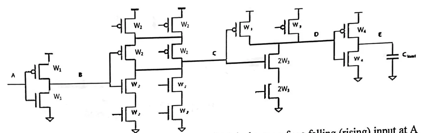
The question (MT23-5, p11, in the paper’s words). Consider the critical path shown below through a set of complementary static CMOS gates. In this technology, the nFET and pFET have the same drive strength and the circuit is sized for equal rising and falling delays. We are working in a technology in which the gate capacitance per unit width is 1 fF/µm. Assume that the FO1 delay is psec. A minimum width device 1.0 µm. Please ignore source-drain diffusion capacitances and overlap capacitances; that is, worry only about the gate input capacitances of the devices. Let pF.
MT23-5’s critical path (p11, redrawn). Nodes A to E as on the paper. Stage 1 is an inverter ; stage 2 an AOI22 with every device ; stage 3 a NAND2 with PFETs and series NFETs ; stage 4 an inverter driving .
The exam’s own figure (MT23-5, p11)
Reading the circuit
Every part needs the same two numbers for each gate, so find them once. The first is its normalized inverter’s input: that measures how strongly the gate drives. The second is the capacitance of one of its inputs: that is the load it puts on the stage before it. The NFET and PFET have equal strength, so an NFET and a PFET of the same width drive equally, and the balanced inverter is W/W.
Why the stack rule. added In the course’s model a conducting transistor is a resistor whose resistance falls as it gets wider: . Current through a stack of two must pass through both, so the resistances add: . Two in series therefore drive like one transistor of half the width. The rule assumes every device in the stack is fully on, which is the worst case of one input switching while the others already conduct. It ignores the extra delay of the node inside the stack (Chapter 8 §10’s bottom-device effect).
The stack rule added: two transistors of width in series add their resistances, , so they drive like one transistor of width .
Reading MT23-5 gate by gate
- Stage 1, an inverter W₁/W₁. An inverter is its own normalized inverter. Its input drives both devices: . So .
- Stage 2, the AOI22, every device W₂. When one input switches, two NFETs in series pull down and two PFETs in series pull up. Two in series act like one of half the width, so the gate drives like a over inverter, whose input is . One real input drives one NFET and one PFET, , so .
- Stage 3, the NAND2. Its two NFETs, each, are in series and act like one of ; a single PFET, , pulls up. So the normalized inverter is , input . That is why the exam drew the NFETs twice as wide: a stack of two devices pulls down as hard as the one PFET pulls up, which is what “equal rising and falling delays” asks for. One input drives , so .
- Stage 4, an inverter W₄/W₄: input , .
- The load: of gate. Converting every capacitance to microns of gate lets each gain be a ratio of widths.
The normalized inverters of stages 2 and 3 added: (a) the AOI22, a stack of two devices in each network, drives like a over inverter, input ; (b) the NAND2, two NFETs in series and one PFET, drives like a inverter, input .
| Stage | Gate | Devices | Acts like (normalized inverter) | One input | |
|---|---|---|---|---|---|
| 1 | inverter | W₁/W₁ | W₁/W₁, input | 1 | |
| 2 | AOI22 | every device W₂, stacks of two in both networks | W₂/2 over W₂/2, input | 2 | |
| 3 | NAND2 | NFETs 2W₃ in series, PFETs W₃ in parallel | W₃/W₃, input | 3/2 | |
| 4 | inverter | W₄/W₄ | input | 1 |
Part (a): the delay as drawn (10 points)
MT23-5a, p11. Estimate the delay of the path from A to E, which is the same for a falling (rising) input at A propagating to a rising (falling) output at E. Let m, m, m, and m. (10 points)
Hint
What it asks. The delay of the path exactly as drawn: a 10 µm first inverter and every other gate at the 1 µm minimum. Nothing is sized yet. The word “estimate” says the gain model is enough; no device equations are needed.
The idea. Each stage takes times its gain, and its gain is the capacitance it drives over its normalized inverter’s input. A stage drives the next stage’s input; the last one drives the load. So read each gain off the table and add them.
Why this formula. added The gain rule is an RC estimate measured against the FO1 inverter.
- Where it comes from. On the falling edge a stage’s output discharges through its pull-down network. In the course’s model a conducting NFET of width is a resistance , so the network acts like the normalized inverter’s NFET, . The capacitance it discharges is everything on the output node, : times the gate width hanging there. The time is proportional to resistance times capacitance: .
- The same for the yardstick. is a W/W inverter driving a copy of itself, : , whatever is.
- Divide. The proportionality constant cancels in the ratio, so : the load, in microns of gate, over the normalized inverter’s input . That is why no 0.69 appears anywhere in this question, and why the exam gives instead of .
- Conditions, and why they hold. Only gate capacitance counts: the exam says to ignore diffusion and overlap. The gates are balanced (the exam says so), so the rising edge, through the PFETs, gives the same gain as the falling one. One input switches through the full stack, the worst case, which is the normalized inverter of the table.
- The tempting alternative. Dividing by the gate’s own input capacitance gives the electrical effort , not the gain. It leaves out the logical effort: for the AOI22 it would give instead of 3, half the true delay.
Where the gain comes from added: on the falling edge the normalized inverter’s NFET is a resistance discharging , so the time goes as . With , a copy of itself, that time is .
MT23-5a
- Stage 4 drives the 1000 µm load. It is an inverter, so its normalized input is its own, m: gain .
- Stage 3 drives stage 4’s input, m. Its normalized inverter is , input m: gain 1.
- Stage 2 drives one NAND input, m. Its normalized inverter’s input is m: gain 3.
- Stage 1 drives one AOI input, m, from its own input m: gain 0.1. A big gate driving a small one has a gain below 1: it is fast, but its size is wasted here.
- Add. Because each stage’s delay is its gain times , the path’s delay is .
Check. A second route to each gain is : the logical effort from the table’s column times the electrical effort , the load over the gate’s own input (not its normalized inverter’s). For the two inverters and the two routes coincide, so the complex gates are the real test. Stage 2, the AOI22: and , so ✓. Stage 3, the NAND: and , so ✓. Gains of 0.1 and 500 in one path are the sign of a badly sized path, which part (b) fixes.
Answer: ns. The last stage’s gain of 500 is almost all of it.
Remember. Gain = load ÷ normalized inverter’s input; delay = × the sum of the gains. Very unequal gains mean the sizes can be improved.
The answer key agrees
Part (b): equal-gain sizing (10 points)
MT23-5b, p12. Assume that is fixed at 1.0 µm but you are free to tune , , and . Find approximate values of , , and to minimize delay and estimate the new delay of your resized network. (10 points)
Hint
What it asks. Choose , and to make the delay as small as possible, with the first inverter fixed at 1 µm, and give the new delay. Fixing fixes the path’s input capacitance. Without that you could make every gate huge and push the problem onto whatever drives A. The words “minimize delay” with one gate fixed and nothing branching decide the method: equal gains.
The idea. Two facts from Chapter 8 do all the work. The product of the gains is fixed, and with a fixed product the sum is smallest when the factors are equal. So every stage gets the same gain, , and the widths follow from it, one stage at a time from the load back.
Why this formula. Part (b) uses four facts. Each is short to derive.
- The gain of each stage is the load over the normalized inverter’s input, as part (a) explains: a stage discharges its load, , through a resistance , where is the width of its normalized inverter’s NFET; dividing by the FO1 inverter’s own RC product leaves , the load in microns of gate over the normalized input. The stage table of Reading the circuit gives the normalized inputs, , , and , and the capacitance of one input, , , and . Each stage drives the next stage’s one input, and the last drives the 1000 µm load, so with the widths as unknowns the four gains are , , , .
- The product of the gains is fixed (Chapter 8 §2). Each inner width appears in two gains: on top in the gain of the stage before it, because it is that stage’s load, and underneath in its own stage’s gain, because it is that stage’s strength. In the product it cancels. What is left depends only on the gate types, the fixed and the load: , with (the four logical efforts) and , with the path’s input capacitance. This needs nothing to branch off the path, which is true here until part (c).
- Equal gains minimize the sum added, and not only for the numbers tried. Change one inner width, say , and leave the others. Only two gains move: stage 2’s gain rises in proportion to , because the NAND is stage 2’s load, and stage 3’s gain falls in the same proportion, because the NAND is stage 3’s driver. Their product, , does not change. For two numbers and with a fixed product , : the sum is smallest exactly when . So at the best , stages 2 and 3 have equal gains. The same holds for (stages 1 and 2) and for (stages 3 and 4). All four gains are then equal, and they multiply to , so each is . Chapter 8’s plot shows the two-stage curve.
- The stack widths added. Translating a normalized inverter back into a gate uses the stack rule. Resistances in series add, , so the NAND’s two series NFETs must each be twice the normalized NFET. That is the in the exam’s figure, and it is why one NAND input presents to the AOI.
- The tempting alternatives. Making every width equal, or every electrical effort equal, is not the rule: gates with a larger logical effort must get a smaller . And starting from the fixed instead of the load does not work: each stage’s load is not known until the next stage is sized.
MT23-5b
- The gains, with the widths unknown. We need them as functions of the widths before we can choose the widths. Each gain is what the stage drives over its normalized input: the inverter drives the AOI’s input from ; the AOI drives one NAND input, , from its normalized input ; the NAND drives the inverter’s from ; the inverter drives 1000 µm from . So the gains are , , , .
- Their product. Because , and each appear once on top and once underneath, they cancel: . (Part (a)‘s gains multiply to , which is with its : a quick check.)
- Equal gains. Because the product is fixed and the sum is smallest with equal factors, each of the four stages gets .
- Size back from the load. Start at the end, because the load is known: the last stage’s equation has only one unknown, and each step back adds only one more. Stage 4 is an inverter, its own normalized inverter, so its gain is the load over its input: gives m.
- Stage 3, the NAND. Its normalized inverter’s input is (the stack of two NFETs acts like ), and it drives the inverter’s input : gives m.
- Stage 2, the AOI. Its normalized inverter’s input is (), and it drives one NAND input, the PFET plus one NFET : gives m.
- Stage 1 is not chosen; it checks the work. ✓. It has to come out equal, because the four gains multiply to ; if it doesn’t, an earlier step has a slip.
- The delay. Four stages at each: .
Check. From 25.2 ns to 1.24 ns: twenty times faster, from resizing alone. A second check that this is a minimum: make the NAND 10% wider, m, with the other widths kept. Stage 2’s gain rises to 6.85 and stage 3’s falls to 5.66, and the delay rises to , as it must just beside a flat minimum. A gain of 6.2 per stage is above the 3–4 that Chapter 8 aims for (Section 4), which says that more stages would help if you could add them (M7’s Question 5c asks exactly that). Here the four gates are fixed.
Answer: m, m, m; delay ns, down from 25.2 ns.
Remember. With nothing branching off the path, is fixed: take , size back from the load, and let the first stage check your arithmetic.
The answer key differs
It gives “1244.7 ns”. The number is right; the unit is ps (1.24 ns).
Part (c): the side load (10 points)
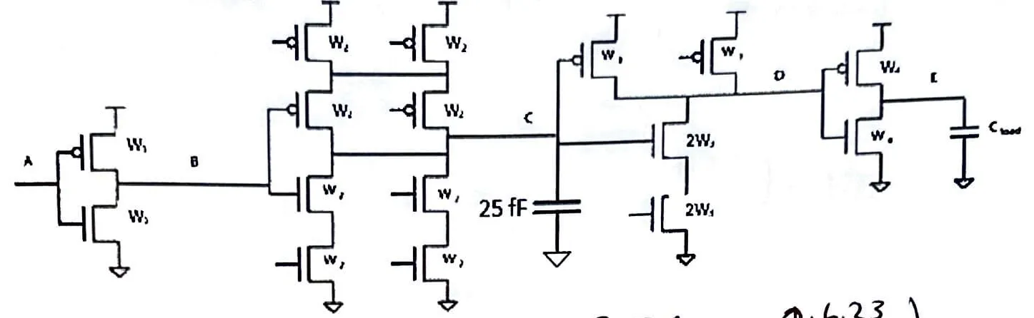
MT23-5c, p13. Now assume that the circuit is modified as shown below. What is the delay of the circuit now from A to E using your sizing from (b)? (10 points)
MT23-5c’s modified path (p13, redrawn): the same four stages, with a 25 fF capacitor from node C, the AOI22’s output, to ground.
The exam’s own figure (MT23-5c, p13)
Hint
What it asks. A 25 fF capacitor is added to the path of (b). Keep the sizes of (b) (, , m) and find the new delay. The first job is to read the figure: which node carries the capacitor?
The idea. A side load is extra capacitance on one node, and each node is driven by exactly one stage. So it raises that one stage’s load, and with it that stage’s gain. Every other stage still drives what it drove before, at the same size, so their gains don’t change.
Why this formula. The gain of the stage driving the node is now its whole load over its normalized inverter’s input. For stage 2 that is , where is the NAND input it drives along the path, is the side load off the path, both in microns of gate, and is the AOI’s normalized input from the stage table. The reason is the same RC estimate as in part (a): the stage discharges every capacitance on its output node through the same resistance, whether that capacitance belongs to the next gate or to a wire. The 25 fF becomes m of gate, because each gain is a ratio of capacitances, and expressing all of them in microns of gate at the same makes them ratios of widths. Only that one gain moves: a stage’s gain depends only on its own size and on what hangs on its own output. The tempting alternatives both fail. Recomputing answers a different question (resizing, which part (d) asks). Putting the capacitor on node D, the NAND’s output, misreads the figure.
MT23-5c
- Find the node. The 25 fF hangs from the wire that runs from the AOI’s output to the NAND’s input (the gates of its PFET and its upper NFET): node C, the output of stage 2.
- Add it to stage 2’s load. At 1 fF/µm it is 25 µm of gate, so stage 2 now drives m.
- Stage 2’s new gain. Its normalized inverter is unchanged, input m: , up from 6.22.
- The other three gains stay at 6.22: their loads and their sizes haven’t changed.
- The delay. Because the delay is times the sum of the gains: .
Check. Chapter 8 gives a second route, through the path effort (Section 8). The path effort is the product of the gains. Without a branch it is ; with one it becomes . Here is the product of the branching efforts of the branched nodes: how many times the whole load on a node exceeds the part that stays on the path. It enters because the branched stage’s gain is times what it would be without the branch, while every inner width still cancels from the product. Only node C branches, so , and with from (b), the new . Step 5’s four gains must multiply to the same number: ✓.
Answer: ns.
Remember. A side load changes one gain: that of the stage driving its node. Find the node first.
The answer key differs
It adds the 25 fF to stage 3’s load (node D), not stage 2’s, and it drops the factor: 1293 “ns”. In the source figure the capacitor is on node C. With the capacitor on D the delay would be ns, and the key’s number fits that reading.
Part (d): retuning (10 points)
MT23-5d, p14. How might this new circuit be resized to reduce the delay calculated in (c), again keeping fixed? Perform this retuning and calculate the new delay. You do not have to achieve a “minimum” delay here; just demonstrate how you would retune the circuit to improve the delay. (10 points)
Hint
What it asks. Resize, with still fixed, to bring the delay of (c) down, and compute it. The exam doesn’t require the minimum, only a sensible retuning, explained. The gains now are 6.22, 10.24, 6.22 and 6.22: stage 2 is overloaded.
The idea. The equal-gain rule of (b) relied on a fixed product of gains. The 25 fF breaks that: it doesn’t grow when the NAND grows, so the path effort now depends on (Chapter 8, Section 8), and a recomputed is only a guess. But the rule still holds on any piece of the path with nothing branching off it. So retune piece by piece:
- Rebalance around the overloaded stage. Stage 2’s gain jumped to 10.24 while stage 1’s stayed at 6.22. Nothing branches between them, so while only moves the product of their two gains is fixed, and the best split is equal.
- Then try enlarging the gate after the branch (the NAND). It lowers stage 3’s gain, and it adds to stage 2’s load only through its own input; the 25 fF stays as it is.
The lecture does these two moves the other way round, enlarging first (Chapter 8, Section 9). That order pays off when the branch is most of the load. Here the 25 fF is only 39% of stage 2’s load, and enlarging the NAND alone (to m) raises the delay to . So rebalance first.
Why this formula. added Two results do the work.
- The pair rule, and where it breaks. As part (b) showed, resizing only the gate between two stages moves only their two gains, and when their product stays fixed, makes the equal split best. Here two of the three pairs still have a fixed product. Stages 1 and 2 share : their gains are and , whose product does not contain . Stages 3 and 4 share : . Stages 2 and 3 share , and their product still contains . A wider NAND raises stage 2’s gain only through the NAND’s share of its load ( of ), while it lowers stage 3’s gain in full proportion. That is why the best gains end up unequal across the branch.
- The split formula. Fix and balance each side. A balanced pair with product has two gains of , so it contributes . The delay is then in , a function of one width that you can tabulate.
- The tempting alternative fails. Recomputing at the current sizes and taking treats as fixed, which a branch makes false; below, it makes the path slower.
MT23-5d
- Rebalance stages 1 and 2. Because the product of their two gains is fixed while only moves, the equal split is best. Their gains are and , whose product is 63.73 whatever is. Equal gains: each, so m.
- The delay now: ns. This one change does most of the work.
- Split the path at the branch added. Because each side of the branch is a branch-free piece, choose a NAND size and balance each side separately. Stages 3 and 4 share the product , and stages 1 and 2 share .
- The delay for a chosen W₃. A balanced pair with product contributes , so the delay is .
- Try a few widths. : 28.41. : 28.28. : 28.27. : 28.44. Take m. The curve is flat near its bottom, so a rough choice is enough.
- The widths. Stages 1 and 2 take each, so m. Stages 3 and 4 take each, so m.
- The delay: ns.
Check. At , the size from (b), the split formula gives 28.41, the same as step 2: the formula contains the first move as a special case. And 28.27 is within 0.01% of the exact minimum with fixed. That minimum comes from imposing all three pair conditions at once: stages 1 and 2 equal, ; stages 3 and 4 equal, ; and the trade across the branch balanced, the NAND’s share of stage 2’s gain equal to stage 3’s gain, , that is . Solved together they give , , m and . Retune it yourself plots the whole curve.
Answer: first m (1.42 ns); then , , m, which gives ns. That is the minimum to within 0.01%. The best gains are not equal: the two stages before the branch share one value (8.54), the two after it a smaller one (5.59).
Remember. With a branch, balance pieces, not the whole path: equal gains still hold on each piece with nothing branching off it. The safe first move is to rebalance the overloaded stage with the one before it.
The answer key differs
It treats the 25 fF as a perturbation: it recomputes at the current sizes, takes and sizes back from the load again, ending at 1292.1 “ns”, with the capacitor on D as in its (c). That method assumes is fixed, and with a branch it is not. Applied to the capacitor where the figure puts it, on C, the method sets and , and it shrinks the gates after the branch. The delay rises to , worse than not retuning (28.91).
2. MT21-5: an input limit and a 500 fF branch (35 points)
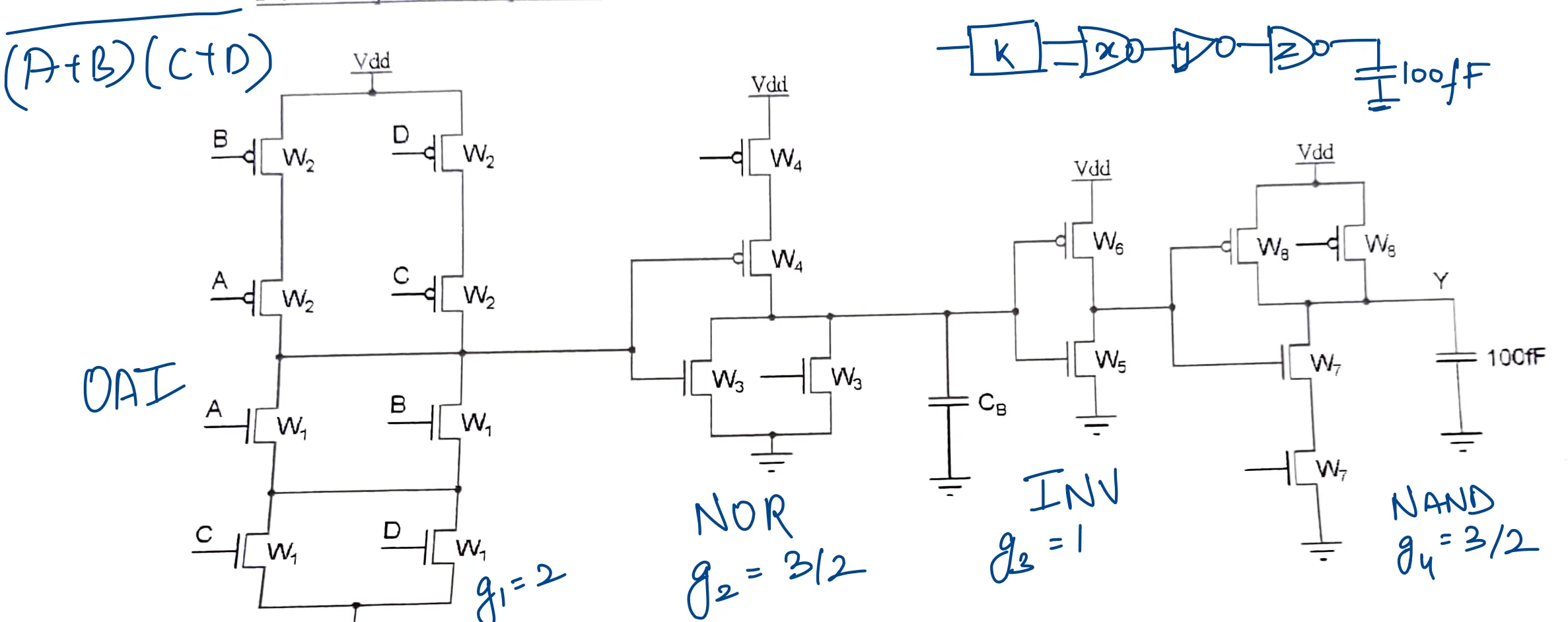
The question (MT21-5, p8). ps and fF/µm. Only gate capacitance counts. The NFET and PFET have equivalent drive strengths. The path runs from A through an OAI gate, a NOR, an inverter and a NAND to Y, which drives 100 fF. A capacitor hangs on the NOR’s output.
Reading the circuit
The same kind of path as MT23-5, with two differences. No gate is given a width: the first gate is limited by its input capacitance instead. And every gate must be balanced by you, so each gate’s two widths are tied together and one width per gate is free. Find the ties and the gains once.
Reading MT21-5 gate by gate
- Stage 1, the OAI22, . When one input switches, the output pulls down through two NFETs in series ( each: A or B, then C or D) and pulls up through two PFETs in series ( each). Both networks act like one transistor of half the width, and the strengths are equal, so the gate is balanced at . It drives like a over inverter, input . One input drives one NFET and one PFET, , so .
- Stage 2, the NOR2. Its two PFETs () are in series and act like ; one NFET () pulls down alone. Balanced means , so . The normalized inverter is , input ; one input drives , so .
- Stage 3, the inverter. Equal strengths balance it at : input , .
- Stage 4, the NAND2. Its two NFETs () are in series and act like ; one PFET () pulls up alone. Balanced means . The normalized inverter’s input is ; one input drives , so .
- The load and the branch. 100 fF at 1 fF/µm is 100 µm of gate. hangs on the wire from the NOR’s output to the inverter’s input: the output of stage 2, the same position as MT23-5’s 25 fF.
| Stage | Gate | Balanced widths | One input | |
|---|---|---|---|---|
| 1 | OAI22, | stacks of two in both networks: | 2 | |
| 2 | NOR2 | PFETs in series: | 3/2 | |
| 3 | inverter | 1 | ||
| 4 | NAND2 | NFETs in series: | 3/2 |
Which edge? A rising A gives a falling OAI output, then a rising NOR output, a falling inverter output and a rising Y. Every gate is balanced, so the falling case has the same gains, and one sum serves both edges.
Part (a): the input limit (15 points)
MT21-5a, p8. With , and the input capacitance of each of A, B, C and D limited to 1 fF, find the sizing for minimum delay from A rising to Y rising (or falling to falling).
Hint
What it asks. Choose all eight widths for the fastest A-to-Y path, with no branch yet (), when each input may present at most 1 fF. The words “limited to 1 fF” decide the method: the cap takes the place of MT23-5’s fixed .
The idea. Same method as MT23-5b (Part (b)): with nothing branching off the path, the product of the gains is fixed, so equal gains make their sum smallest. What is new is that you must choose the first gate’s size. The fixed product is the path effort (Chapter 8, Section 2):
is the cost of the gate types, and , the path’s electrical effort, is the load over the path’s input capacitance. It holds when nothing branches off the path. Here , so a larger input means a smaller and a faster path. The cap exists because the input is the load on whatever drives A, outside the path: without it you would make every gate huge and push the delay onto that driver.
MT21-5a
- Use the whole input limit. Because falls as grows, take fF, which is m. The balance gives m.
- The path effort. and , so .
- Equal gains. Four stages share it equally: .
- Size back from the load, because the load is the one capacitance known at the end. Write each gain as , with the stage’s one-input capacitance: that is the same number as the load over the normalized inverter’s input, because one input is times that. NAND: gives m, so m and m.
- Inverter: gives m, so m.
- NOR: gives m, so m and m.
- The OAI checks the work. Its gain is . ✓ It has to be, because the four gains multiply to .
- The delay. ns.
Check. Use only half the limit, 0.5 fF, and doubles to 900: the delay becomes , 19% slower. The delay grows as , so the whole limit is worth taking, and it is the only thing that sets the first gate’s size.
Answer: , , , , , m; delay ns. Using the whole input limit is the lecture’s point that is set from outside the path (Chapter 8 §2).
Remember. When a question caps the input instead of fixing a width, is smallest at the cap: use all of it, then size back from the load as with a fixed first gate.
The answer key agrees
It gives the same sizes; it doesn’t state the delay.
Part (b): a 500 fF branch (20 points)
MT21-5b, p9. Now fF. Find a sizing close to the minimum delay from A rising to Y rising (or falling to falling).
Hint
What it asks. Hang 500 fF on the NOR’s output and resize for a delay close to the minimum. The OAI’s input stays at the 1 fF limit. “Close to the minimum” means that a sensible retuning, explained, is enough.
The idea. Same retuning as MT23-5d (Part (d)): the branch makes depend on the sizes, so is no longer the answer, but equal gains still hold on any piece of the path with nothing branching off it. What is different is the branch’s size: 500 µm against the inverter’s 7 µm, 99% of the NOR’s load. That decides which move pays (Chapter 8, Section 9).
- Rebalance first. At (a)‘s sizes the NOR, sized for 7 µm, now drives 507 µm: its gain is 330. The lecture’s example enlarges the gate after the branch first, but its branch driver was already sized for the branch. Here enlarging the inverter first (to ) would add to that huge gain, to 345, and the delay would rise to , worse than doing nothing.
- Then enlarge the gate after the branch: here it pays. Split the path at the branch (the split of step 4) added. The pair before it shares the product , the pair after it . Because the branch dominates, quadrupling the inverter raises the first product by only 4.5% (1521 to 1590) and divides the second by 4.2 (21.2 to 5). That is the lecture’s “drop this gain far more than I increase this gain” in its strongest form. In MT23-5d, where the branch was 39% of the load, the same move saved ; here it saves .
MT21-5b
- See what the branch does at (a)‘s sizes. A side load adds only to the stage that drives its node, so only the NOR’s gain changes. It drives m from its 2.30 µm input: gain . The delay is ns. The branch is 99% of the NOR’s load.
- Rebalance the pair before the branch. The OAI’s input is fixed and nothing branches between the OAI and the NOR, so while only the NOR moves, the product of their two gains stays at . Equal factors give the smallest sum: each. The OAI’s gain is , so the NOR’s input is m: m and m.
- The delay now: ns, already a factor of four better.
- Split the path at the branch added. Because the inverter’s input is under 2% of the NOR’s load, enlarging it costs the NOR little and makes the last two stages cheap. With the inverter’s input , the pair before the branch shares and the pair after it shares .
- The delay for a chosen W₅. A balanced pair with product contributes , so the delay is .
- Try a few widths. Growing the inverter raises the cost of the pair before the branch (its input adds to the NOR’s load) and lowers the cost of the pair after it; the best is where those two changes match. : 87.2. : 84.9. : 84.2. : 85.1. Take m.
- The pair before the branch: each. The NOR’s input is m, so m and m.
- The pair after it: each. The NAND’s input is m, so m and m.
- The delay: ns.
Check. A floor. Whatever the sizes, the pair before the branch must carry a product of at least , so it costs at least . No sizing reaches that, because the stages after the branch would have to cost nothing; 84.2 is within 9% of it.
Answer: , , , , , m; delay ns. That is the exact minimum to three figures. The rebalance of step 2 alone (8.72 ns, step 3) is already “close to the minimum”. Most of the delay is the cost of driving 500 fF from a 1 fF input, which no sizing removes.
Remember. With a heavy branch, first share the overloaded stage’s gain with the stage before it. Then enlarge the gate after the branch: the larger the branch’s share of the load, the more that move buys.
The answer key differs
It gives 9.16 ns, with , and m. It minimizes its delay expression with partial derivatives. That is added calculus: the lecture says the retuning can be done exactly but usually “you just sort of look at it” (L08 52:20–53:19). Its algebra slips in two places.
- Its final polynomial has 12 where belongs. With 1728 the root is m, not 106.
- Its balances only the first two stages. It does not satisfy its own , which gives about 89 at .
Its sizes give ns, 9% above the minimum. The method would earn credit; the numbers are off.
3. MT17-5: unequal strengths and a branch inverter (40 points)
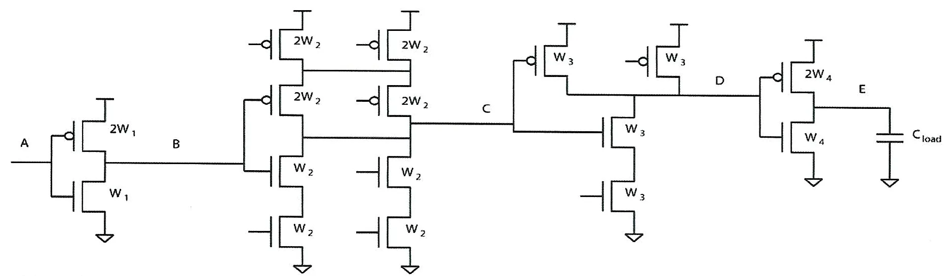
The question (MT17-5, p10). A critical path through complementary static CMOS gates. Each gate is sized for balanced rise and fall, with the PFET having half the drive strength of the NFET. fF/µm, ps, a minimum device is 1.0 µm, and pF. Only gate capacitance counts.
Reading the circuit
The same four gate types as MT23-5. What is different is the strength convention: the PFET has half the NFET’s drive (), so a PFET must be twice as wide to pull as hard, and every normalized inverter has the 2:1 shape.
Reading MT17-5 gate by gate
- The reference inverter. With , an inverter pulls up as hard as it pulls down when its PFET is twice its NFET: 2W/W, input . Its FO1 delay is the the exam gives.
- Stage 1, an inverter 2W₁/W₁. It is its own normalized inverter: input , .
- Stage 2, the AOI22: NFETs , PFETs . When one input switches, two NFETs in series pull down, like one NFET of , and two PFETs in series pull up, like one PFET of (half of ). So it drives like a over inverter, 2:1 as required, input . One input drives one NFET and one PFET, , so .
- Stage 3, the NAND2: every device . Its NFETs are in series and act like ; one PFET, , pulls up alone. over is again 2:1, so the gate is balanced, and its normalized inverter’s input is . One input drives , so . That is less than the 3/2 of equal strengths, because the NAND’s stacked devices are now the strong ones.
- Stage 4, an inverter 2W₄/W₄: input , .
- The load. is 2 fF/µm here, not 1: m of gate.
| Stage | Gate | Devices | Normalized inverter | One input | |
|---|---|---|---|---|---|
| 1 | inverter | 2W₁/W₁ | input | 1 | |
| 2 | AOI22 | NFETs W₂, PFETs 2W₂, stacks of two in both | W₂ over W₂/2, input | 2 | |
| 3 | NAND2 | NFETs W₃ in series, PFETs W₃ in parallel | W₃ over W₃/2, input | 4/3 | |
| 4 | inverter | 2W₄/W₄ | input | 1 |
The AOI22 is the gate of Chapter 8’s check (§1).
Part (a): the delay as drawn (10 points)
MT17-5a, p10. Estimate the A-to-E delay with every m.
Hint
What it asks. The delay of the path exactly as drawn, with every at 1 µm. The drawn factors still apply: the inverters’ PFETs are 2 µm.
The idea. Same method as MT23-5a (Part (a)): each stage takes times its gain, the capacitance it drives over its normalized inverter’s input, and the path delay is times their sum. Only the table changes with the 2:1 convention: an inverter’s input is , and a gate’s one input is larger than its normalized input by its .
MT17-5a
- Stage 4 drives the 600 µm load from its normalized input m: gain .
- Stage 3 drives stage 4’s input, m, from m: gain .
- Stage 2 drives one NAND input, m, from m: gain .
- Stage 1 drives one AOI input, m, from m: gain .
- Add. Delay .
Check. The last stage is 200 of the 204.3, 98% of the delay: a 3 µm-input inverter driving 600 µm is driving 200 copies of itself. In units, ps is 20.4 ns.
Answer: ns.
Remember. With , the inverter’s input is and every normalized inverter is 2:1. After that, the gains are read exactly as with equal strengths.
The answer key agrees
It writes “Stage 1: gain = 3/2 = 1”. The fraction should be 3/3; its result, 1, is right.
Part (b): equal-gain sizing (10 points)
MT17-5b, p11. is fixed at 1.0 µm; tune , and for minimum delay, and estimate the new delay.
Hint
What it asks. Choose , and for the smallest delay, with the first inverter fixed at 1 µm, and give the new delay.
The idea. Same method as MT23-5b (Part (b)): the inner widths cancel in the product of the gains, which leaves a fixed path effort ; with a fixed product, equal gains give the smallest sum; size back from the load. New here: and . Keep as a fraction until the end.
MT17-5b
- The gains, with the widths unknown: , , , .
- Their product. Each inner width appears once on top and once underneath, and cancels: . That is , and also (a)‘s gains multiplied: .
- Equal gains: .
- Size back from the load, because the last equation has only one unknown: gives m.
- gives m.
- gives m.
- Stage 1 checks the work: . ✓
- The delay: ns.
Check. From 20.4 ns to 1.92 ns: about 10.6 times faster, from resizing alone. A gain of 4.8 per stage is a little above the 3–4 that Chapter 8 aims for (Section 4), so four stages are about right for this load.
Answer: , , m; delay ns.
Remember. The strength convention changes only the table; the recipe (, , back from the load, stage 1 checks) is the same.
The answer key agrees
It gives , because it multiplies by 1.33 instead of ; the exact value is 533.3. Its rounded widths (41.7, 17.4, 4.8 µm) and its 1.92 ns are fine. Its stage-1 line writes “3W₃/2W₁” for .
Part (c): a branch inverter (10 points)
MT17-5c, p12. The circuit is modified as shown. What is the delay with the sizes of (b)?
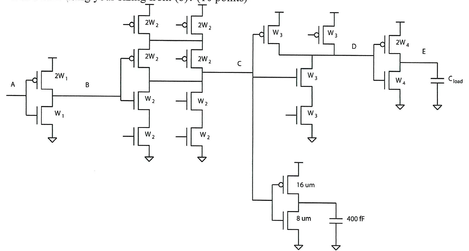
Hint
What it asks. An inverter (PFET 16 µm, NFET 8 µm) driving 400 fF is hung on node C. Keep (b)‘s sizes and find the new delay. Two readings decide it: which node, and which part of the new inverter loads the path.
The idea. Same rule as MT23-5c (Part (c)): a side load raises only the gain of the stage that drives its node. What is new is that the side load is a gate, not a capacitor. Node C sees only that gate’s input, m of gate. The 400 fF sits on the branch inverter’s own output. Charging it is that inverter’s job, on the path from C to its output; the A-to-E signal passes C into the NAND and never waits for it. Counting the 400 fF on node C is the trap.
MT17-5c
- Find the node. The new inverter’s input is wired to C, the output of stage 2 (the AOI).
- Count its input only. Its gates are m. Its own 400 fF load is behind it, off the A-to-E path, so it doesn’t count here.
- Stage 2’s new gain. It now drives m from m: gain , up from 4.81.
- The other three gains stay at 4.81, because their loads and their sizes haven’t changed.
- The delay: .
Check. The delay rose by , exactly the rise in stage 2’s gain (): nothing else moved. The branch is 41% of stage 2’s load, and the branching effort at C is (Chapter 8, Section 8).
Answer: ns.
Remember. A gate hung on a node loads it with its input only; whatever that gate drives is off the path.
The answer key agrees
It gets 8.17 for stage 2’s gain, from its rounded widths (17.4 and 4.8 µm), and the same 2.26 ns.
Part (d): retuning (10 points)
MT17-5d, p13. Keeping fixed, resize to reduce the delay of (c) and compute the new delay. The minimum isn’t required.
Hint
What it asks. With still fixed, resize to bring the delay of (c) down, and compute it. A sensible retuning, explained, is enough.
The idea. Same retuning as MT23-5d (Part (d)): the branch makes depend on the sizes, but equal gains still hold on each piece with nothing branching off it. The branch is 41% of stage 2’s load, close to MT23-5’s 39%, so as there, rebalance first: enlarging the NAND alone (to m) would raise the delay to . The new thing here is the trap the key falls into: resizing only the stage that drives the branch. That stage’s input is stage 1’s load. While only moves, the product of the two gains is fixed, so a larger only shifts gain from stage 2 to stage 1; the best split is the equal one (Chapter 8, Section 9).
MT17-5d
- The trap, worked out. Resizing only stage 2 so that its own gain is back to 4.81 needs m. But stage 1 drives , so its gain becomes . The delay is still : the excess gain just moved one stage back (Chapter 8 §9).
- Rebalance instead. Because and are fixed and nothing branches between stages 1 and 2, their product is fixed: . Split it equally: each, so m.
- The delay now: ns.
- Then enlarge the gate after the branch added. Split the path at the branch, as in MT23-5d. Stages 3 and 4 share ; stages 1 and 2 share . Balancing each pair gives a delay of .
- Try a few widths. : 22.12. : 22.01. : 21.99. : 22.05. Take m.
- The widths. m, and stage 4’s gain is , so m.
- The delay: ns.
Check. The trap’s two gains, 8.14 and 4.81, multiply to 39.1, the same product as 6.25 × 6.25. With the product fixed, the unequal pair sums to 12.9 and the equal pair to 12.5: that difference is all that step 2 gains, and the trap gains nothing.
Answer: m gives 2.21 ns; with and m as well, m and the delay is ns, the minimum. The branch is only 41% of stage 2’s load, so the gain is small: the 1.92 ns of (b) cannot come back.
Remember. Never fix a branch by resizing only the stage that drives it: its input is the load of the stage before. Rebalance that pair, then try a larger gate after the branch.
The answer key differs
It resizes stage 2 to a gain of 4.8 (m) and says that the “delay is now back to 1.92 nsec”. That is the trap of step 1: stage 1’s gain becomes 8.17, so the delay stays at 2.26 ns. Its closing remark, that more can come from sizing up stages 3 and 4, points the right way.
4. Retune it yourself
The widget sizes each of the three paths the way the steps above do. Pick the size of the gate just after the branch; the stages before the branch then share one equal gain, and the stages after it share another. The curve is the delay for every such choice. Its lowest point is the exact minimum with the first gate fixed.
What to notice.
- At the (b) or (a) sizes, the curve already gives the “rebalance the pair” delay. For MT21-5 that single move removes 75% of the delay.
- The curves are flat near their minima: an approximate size is enough, as the exam asks.
- MT21-5’s best inverter is several times its (a) size, because the branch dominates the NOR’s load. MT17-5’s and MT23-5’s branches are smaller (41% and 39% of the load), and the best gate after the branch grows only by about 25%.
added Splitting a path at its branch is this guide’s way of organizing the lecture’s two moves (enlarge the gate after the branch, then rebalance). Each piece is an ordinary path with nothing branching off it, so Chapter 8’s equal-gain rule applies to it.
Patterns
Path sizing in one box. The reasons are in How to approach a path-sizing question.
- Read the circuit first: the strength convention (W/W or 2W/W), each gate’s normalized input and one-input capacitance, the load in µm of gate, and the node a side load hangs on.
- (a) Gains as drawn, delay gains. (b) , , size back from the load, and let stage 1 check the arithmetic. (c) Recompute only the gain of the stage that drives the branch.
- (d) Rebalance the overloaded stage with the one before it, then try a larger gate after the branch. That second move pays most when the branch is most of the load (MT21-5b).
- Traps: the branch on the wrong node (MT23-5c’s key); ps against ns (MT23-5b–d’s keys); resizing only the stage that drives the branch (MT17-5d’s key); treating a recomputed as fixed (MT23-5d’s key); counting what a branch gate drives instead of its input (MT17-5c).
- No exact minimum is needed. The lecture retunes by inspection; three or four widths in the two-pair formula are enough.
- Time. About 15–20 minutes for 35–40 points. Parts (a)–(c) are mechanical (3–4 minutes each). Spend the rest on (d), and explain the move in words: the exams give partial credit for the reasoning.