F4. Past finals: pass-transistor and dynamic logic
The past finals cover the whole course, but several of their questions are on the midterm’s dynamic and pass-transistor logic (Lectures 7 and 10–12). This page re-solves those parts: three on dynamic and domino gates, then two on pass-transistor and differential networks. They give the two midterm families of pages M5 and M6 more practice, with circuits the midterms have not used: a gate with no clock that resets itself, charge sharing, a stage that drives a PFET network directly, and a pass network that counts.
Every answer below is re-solved here; none is copied from an answer key. Where a key disagrees or leaves something out, the folded note on the key at the end of the part explains it, and the table at the end lists them all.
After this page you can:
- state the conditions a footless dynamic gate puts on its input waveforms, and describe the output of a gate that resets itself;
- compute charge sharing between a dynamic node and an internal node, judge whether it can falsely evaluate a domino gate, and name the fixes with their costs;
- read a two-stage dynamic circuit with a p-type second stage (NP domino): the phase in which each stage evaluates, and its function;
- read the function of a differential gate with cross-coupled PFETs, and say what those PFETs do;
- trace a pass-transistor network for every input, find the nodes that float, and write a static CMOS network for the same function.
Before you start
How to use this page. Each section restates one exam question with its source page (FN12-5a, p7 is the Fall 2012 final, question 5a, physical PDF page 7) and its points, and shows the exam’s own figure. The two families are taught on the midterm pages, in M6’s dynamic-logic approach and M5’s pass-transistor approach: how to recognize the question, the moves in order, why the rules apply, and the traps. Each part here says what it adds to them. Then every part is worked the same way: what it asks, the idea behind the method, the solution in steps (each step gives its reason first), a check on the result, the answer, and one thing to remember. Try each part on your own first; open the Hint if you are stuck, and step through the solution before you press “Show all”. The answer key’s verdict is folded at the end of each part. The chapters teach each method in full, and every solution links the section. The finals were 180-minute exams of 200 or 250 points, so they allow about 45–55 seconds a point, about twice the midterm’s pace.
| Question | Family | Parts | Points | Chapters | Midterm page |
|---|---|---|---|---|---|
| FN17-11 | dynamic | input and output waveforms | 10 (of 250) | 11, 12 | M6 |
| FN17-2 | dynamic | race, collision, function | 25 (of 250) | 11, 12 | solved on M6 |
| FN12-5 | dynamic | charge sharing, fixes | 22 (of 200) | 6, 11 | M6 |
| FN12-10b | dynamic | clock phases, function | 9 (of 200) | 11, 12 | M6 |
| FN12-10c | pass-transistor | function | 9 (of 200) | 7, 10 | M5 |
| FN10-7 | pass-transistor | function, static CMOS | 20 (of 200) | 7, 10 | M5 |
The other parts of these finals (FN12-10a, a PLA, and FN12-10d, a decoder table, among them) are on topics after the midterm and are left out.
Conventions
- n-type and p-type stages (Chapter 11, Section 4; Chapter 12, Sections 5–6). An n-type stage is precharged to 1 and evaluates through NFETs; its node is , where is the network’s conduction function. A p-type stage is pre-discharged to 0 and evaluates through PFETs, which conduct on 0s; its node is .
- Edges. In evaluate an n node can only fall and a p node can only rise; a node that has moved cannot come back until the next precharge. Each answer below says which edge it is about.
- Levels (Chapter 10, Section 5). An NFET passes 0 cleanly and a 1 only as ; NFETs in series whose gates are at lose one threshold in all, not one each.
- Names. The exams’ names are kept. Added names: X for FN17-11’s dynamic node, M1–M18 for FN10-7’s transistors.
1. FN17-11: a dynamic OR that resets itself
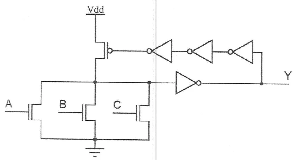
FN17-11, p23 (Fall 2017 final, 10 points). Consider the dynamic gate shown below. What properties must the waveforms at A, B, C have to ensure correct functionality (including no collisions) of this circuit as a three-input OR gate? What properties does the output waveform Y have?
Hint
What it asks. Two lists of properties: what the waveforms at A, B and C must do for the circuit to work as a three-input OR, and what the output Y then looks like. The words “no collisions” decide the main condition.
The idea. Read the gate with the moves of M6’s dynamic-logic approach: what precharges the node, what the node computes, and which hazard the stage has. Its move 7 is the one that matters here: a footless stage must not precharge while an input is 1, and this gate has no footer, so every input must be back at 0 before the PFET turns on. What is new is that there is no clock. The PFET that precharges X is driven from the gate’s own output, through three inverters, so the gate resets itself a fixed time after it has fired. Lecture 11 resets dynamic gates with a clock and Lecture 12 delays that reset; a gate that times its own reset goes a step beyond the lectures, but every rule needed to read it is theirs:
- a dynamic node that has been discharged stays down until the next precharge (Chapter 11, Section 4);
- a footless stage collides if an input is still 1 when precharge begins (Chapter 11, Section 4).
So first find when the PFET turns on and off. Then hold each input condition against those times, and read Y off the same timeline.
How the circuit behaves
- At rest, the PFET is off. Start from rest, because every condition is measured from it. A, B and C are 0 and X is high, so Y = 0. Three inverters make the PFET’s gate , so the PFET is off. X is held by nothing, a dynamic node, exactly as in the evaluate phase of Chapter 11, Section 4.
- Evaluate. X floats high with nothing holding it, so when any input rises, its NFET discharges X, and Y rises. The NFETs are in parallel, so Y = A + B + C: a dynamic NOR followed by an inverter, a domino OR (Chapter 11, Section 6). There is no footer.
- Reset. The PFET’s gate follows Y through three inverters, so three inverter delays after Y rises, the PFET’s gate falls and the PFET turns on. It recharges X; Y falls; three inverter delays later the PFET turns off again, and the gate is back at rest. The gate precharges itself, a fixed time after it has evaluated: the delayed reset of Chapter 12, Section 7, with the inverter chain as the delay.
What the inputs must do
- Rise once, cleanly, from 0. Nothing but the reset brings X back up, so an input that rises, even briefly, discharges X for good (Chapter 11, Section 4). A glitch on any input fires the gate. So the inputs must be 0 at rest and make only a clean rising pulse: no glitches, no hazards.
- Stay high long enough. Y rises only once X has fallen through the output inverter’s switching threshold, so a pulse must last at least that long (the evaluate delay). A shorter pulse leaves X part-way down: Y may not rise at all, and the lost charge stays on X as noise.
- Be back at 0 before the PFET turns on. The gate has no footer, so an input still high when the PFET turns on gives a collision: current from to ground, and X held between the rails (Chapter 11, Section 4). This is the lecture’s condition for leaving the footer out: every input must be back at 0 before precharge begins (Lecture 11, 19:40). Here precharge begins one loop delay after the first input arrives: the evaluate delay, the output inverter, then three inverters.
- Not rise again while the PFET is on. The same collision happens whenever an NFET conducts while the PFET is on. The PFET stays on until three inverter delays after Y has fallen.
- Arrive together. The gate makes one Y pulse per evaluation, so an input that rises after the reset has finished starts a second evaluation, a second Y pulse: a separate OR, not part of this one. So for one OR of A, B and C, every input that is 1 must pulse inside the same window: its rising edge after the gate is at rest, and its falling edge before the PFET turns on. In practice the pulses overlap.
What the output Y does
- One pulse per operation. Y is the inverse of X, and X falls once and is recharged once per operation. So Y is 0 at rest and makes one positive pulse per operation: a pulse if any input pulsed, none if all stayed at 0. It is the OR of the inputs, carried as a pulse.
- It rises with the earliest input. The NFETs are in parallel, so the first input to rise starts the discharge: Y rises one evaluate delay plus one inverter delay after the earliest input edge. Later inputs in the same window change nothing.
- It falls by itself. Only the loop recharges X, so Y falls after one trip round it: three inverter delays, the PFET’s recharge of X, and the output inverter. Its width is set by the circuit, not by the inputs: a wider input pulse (inside the limits above) does not stretch Y. It only lets X fall further before the reset, so the recharge takes a little longer.
- It can drive another such gate. added Y is a clean, glitch-free pulse that starts at 0, which is just what the inputs had to be. So Y can drive another gate of this kind, provided its pulse fits that gate’s window.
- Left idle, it can fire by itself. added Between operations X floats high with no half latch drawn, so leakage slowly drains it (Chapter 11, Section 8). Left idle long enough, the gate would fire a false Y pulse on its own (and then reset itself). A half latch on X, driven from Y, would hold it.
Worked numbers. added The exam gives no delays. For example, with illustrative values chosen for the widget below: the pull-down takes X to half in 30 ps, each inverter takes 20 ps, and the PFET recharges X to half in 30 ps. Measured from the earliest input edge: Y rises at ps; the PFET turns on at ps, so every input must last at least 30 ps and be back at 0 by 110 ps; Y is at most about ps wide, whatever the inputs did (a little less when X has not fallen all the way); the PFET turns off about 60 ps after Y falls, near 220 ps, and only then may the next operation start.
Check. The input conditions must leave room for a valid input, and they do. An input that starts the operation must last at least the evaluate delay, and must end before the PFET turns on, the evaluate delay plus four inverter delays after it rose. So its window is longer than the minimum width by the four inverter delays, whatever the delays are: 80 ps with the worked numbers (110 against 30 ps). The inverters in the loop are what buy the inputs their slack; a shorter loop would leave less.
Answer: Inputs: clean, glitch-free pulses from 0 (monotonic: one rising edge, then back to 0); each at least as long as the evaluate delay; all the pulses of one operation inside one window, so in practice overlapping; every input back at 0 before the feedback turns the PFET on (about the evaluate delay plus four inverter delays after the first edge), and none rising again until the PFET has turned off. Output: Y is a single positive pulse, the OR of the input pulses, that starts about one evaluate delay and one inverter delay after the earliest input and ends by itself; its width is set by the loop (about three inverter delays, the recharge and the output inverter), not by the inputs’ widths.
Remember. A dynamic gate without a clock still follows the clocked rules: monotonic inputs, back at 0 before precharge begins. When the gate resets itself, the loop’s delay sets both the inputs’ window and the output’s width. Recognize it by a precharge device whose gate comes from the gate’s own output.
The answer key differs
It says “Waveforms at A, B, C must be pulses that overlap. Waveforms at A, B, and C must reset before the inverter chain activates the pFET device.” Both statements are right. It doesn’t say how long a pulse must last, that the inputs must be glitch-free, or that they must not rise again while the PFET is on, and it has no answer for the second question, on Y.
What to notice.
- With B at 0 width, take A from 45 to 100 ps: A’s pulse grows by 55 ps, Y’s by about 14 ps (91 to 106 ps), only because X falls further and takes longer to recharge. Y never outlasts the loop.
- “A too long” and “B too late” both collide (red): one because an input outlasts the window, the other because it starts after the PFET has turned on.
- “B after the reset”: a second Y pulse. The gate has computed two ORs, not one.
- “A too short”: no output, and X is left part-way down with nothing to restore it.
- Slow the inverters: the window for the inputs grows, and so does Y’s width.
Check yourself In FN17-11, a designer replaces the chain of three inverters by a chain of five, to give the inputs more time. What happens to the window for the inputs and to Y? Why must the chain have an odd number of inverters?
The PFET turns on two inverter delays later, so the inputs may stay high longer, and Y is two inverter delays wider (each pulse occupies the gate longer, so operations must be further apart). The chain must invert: the PFET must be off while Y = 0 (at rest, X must be left floating high for the inputs to discharge) and on while Y = 1. With an even number of inverters the PFET’s gate would equal Y: on at rest, so any input would collide, and off after evaluating, so X would never be recharged.
2. FN17-2: two dynamic stages on two clocks
FN17-2, p4–5 (Fall 2017 final, 25 points). Two footed dynamic NAND2s on (all devices 1 µm) drive a footless dynamic NOR2 on (5 µm NFETs, a 1 µm PFET, 50 fF on Y) directly, with no inverters; ps, 2 fF/µm. (a) How must rise relative to to avoid a race? (b) How must it fall to avoid collisions? (c) The function, and the delay from A rising to Y falling.
What it asks. How the second clock must rise (a race) and fall (a collision) against the first when two bare dynamic nodes drive a footless stage, then the function and one delay. Page M6 re-solves it in full: M6, Section 5. Compare FN12-10b below, where a bare dynamic node can drive the next stage directly, because that stage is p-type.
Answer: (a) must rise at least 500 ps after (stage 1: , ). (b) With bare dynamic nodes driving a footless stage, no timing of the falling edges avoids the collision: and precharge to 1, so delaying ‘s fall makes the collision certain; the fix is a footer. (c) Y = ABCD. A rising cannot make Y fall (it turns a NOR NFET off); Y’s falling evaluation takes 167 ps after rises, 667 ps after .
The answer key differs
It says 556 ps in (a) (it rounds 1/3 µm to 0.3 µm), “ falls 333 ps after ” in (b) (the delayed-reset rule, which needs inverters between the stages), and 723 ps “from A rising to Y falling” in (c), an edge pair the circuit cannot make.
3. FN12-5: charge sharing in a domino gate
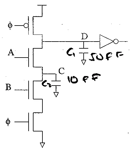
FN12-5a, p7 (Fall 2012 final, 12 points). Assume that the gate is in evaluate () and that initially inputs A and B are grounded, node C is at ground, and node D is precharged to V. Let the total capacitance of node D be 50 fF, and let the total capacitance of node C be 10 fF. If A switched from low to high, what will be the final voltage value on node D? What consequence might this have on the functioning of this circuit?
Hint
What it asks. The voltage left on the dynamic node D when A rises but B stays at 0, so that the gate should not evaluate, and what that voltage might do to the gate. “Node C is at ground” is the condition that decides it: the internal node starts empty.
The idea. This is the noise move of M6’s dynamic-logic approach: the inverter after a dynamic node is skewed toward its logic edge, which shrinks the margin that protects the node’s resting value. What is new is the source of the noise, charge sharing (Chapter 11, Section 10). With no path to ground, no charge can leave D; but when A turns on, D’s charge spreads over D and C together. Charge is conserved, so the shared voltage is
where and are the total capacitances of the two nodes. It holds while A conducts the whole way: an NFET can raise C only to , one threshold below its gate. Then hold the drooped level against the inverter’s switching threshold.
FN12-5a: where the charge goes
- Is there a path to ground? B stays at 0, so no: D should stay at 1. But A turns on and connects D to C, which is empty (Chapter 11, Section 10).
- Count the charge before, because it is all there will be afterwards: on D, nothing on C.
- Share it. No charge has left, so it now sits on both nodes at one voltage: , a drop of 0.42 V.
- Check that A lets C rise that far. C rises to that 2.08 V through A, an NFET with its gate at 2.5 V, which can pass up to . So the answer holds for any below 0.42 V. With a larger , C stops at and D keeps more: at V, C stops at 2.0 V and V. added
- The consequence. The inverter after D is skewed toward its PFET, because its rising output carries the logic (Chapter 11, Section 7). That raises its switching threshold and shrinks D’s high noise margin. If the threshold is above the drooped level, the output rises: a false evaluation, which cannot be undone until the next precharge.
- Does this droop alone flip it? added It depends on the skew, so put in one. Take Chapter 12’s 8:1 inverter (four times the NFET’s strength) and, for illustration, square-law devices with V (Chapter 6, Section 4): it switches where , at V. So 2.08 V is still read as a 1, but only 0.55 V of margin is left for leakage, coupling and supply noise, which add.
Check. Charge is conserved: after sharing, , the 125 fC that D held alone. ✓ The drop is the fraction of : a small internal node costs little, one as large as D would halve it.
Answer: V (if C may rise that far, V). The 0.42 V loss is charge-sharing noise; the skewed domino inverter switches above and may read the node as 0, a false evaluation that lasts until the next precharge.
Remember. With no path to ground a dynamic node can still droop: it shares its charge with an internal node and keeps the fraction of . Hold the drooped level against the skewed inverter’s threshold, not against .
The answer key agrees
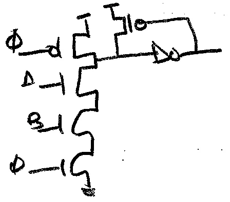
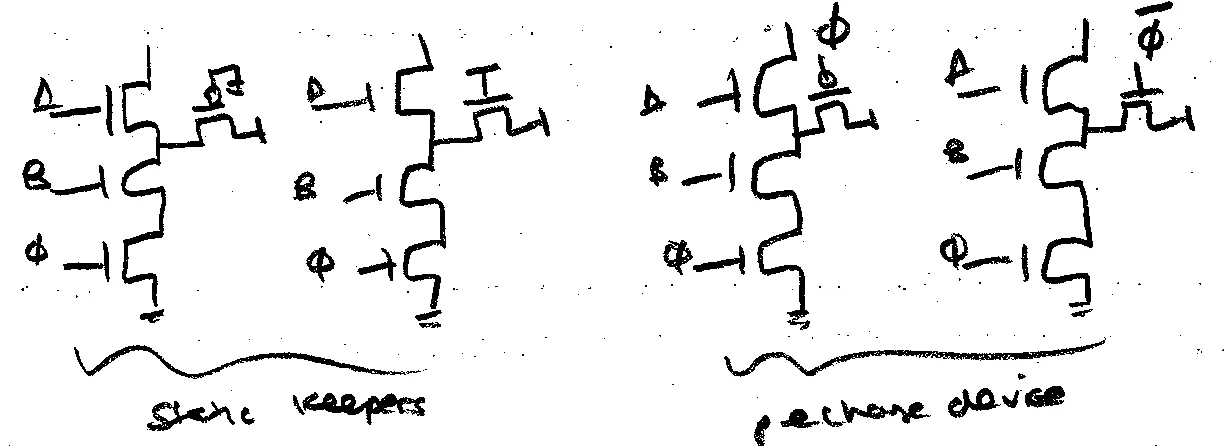
FN12-5b, p8 (10 points). Describe at least two circuit changes that can be used to mitigate the effects noted in (a).
Hint
What it asks. At least two circuit changes that reduce the charge-sharing droop of (a), and, for full credit, what each one costs. “Mitigate” means the gate must still evaluate correctly when A and B are both 1.
The idea. Part (a) found two causes, so there are two places to act. At D, put back the charge it loses: the half latch, the fix M6’s MT23-3d uses for a p node, here in its original form for an n node (Chapter 11, Section 8). At C, make sure the node is already full, so there is nothing to share: Lecture 11’s babysit devices (Chapter 11, Section 10). Each fix adds charge that a real evaluation must later remove, so each must be weak or clocked, and each costs some speed.
FN12-5b: the fixes and their costs
- A half latch on D (Chapter 11, Section 8). D must keep its charge, so feed it back: a weak PFET from to D, its gate on the inverter’s output. While the output is 0 it holds D up and puts back the charge that C took. Cost: every real evaluation must fight it, so keep it weak, about one tenth of the pull-down (Section 9).
- Precharge node C (Chapter 11, Section 10). An empty C is what takes the charge, so fill it during precharge: a small PFET on from to C, or an NFET on (to ). C then starts full, and there is nothing to share. Cost: more power in precharge, more load on the clock, and a real evaluation must also discharge C, so it is slower.
- A weak device that always holds C up. To fill C without a clock, use a device that is always on: a PFET with its gate grounded, or an NFET with its gate at . No clock load, but it fights every real evaluation, so it must be weak.
- Prefer NFETs for the devices on C, because a PFET among the NFETs of the stack needs its own N well, a layout pain (Lecture 11, 44:22). The devices of steps 2 and 3 are the lecture’s babysit devices (46:44).
- added Skew the inverter less. The droop matters only against the inverter’s threshold, so lowering the threshold leaves D more margin, at the price of a slower rising output.
Check. Each fix must pass two tests: (a)‘s case (A rises, B = 0) leaves D high, and a real evaluation (A = B = 1) still pulls D to 0. The half latch and the always-on device pass the second only because they are weak; the clocked devices on C pass it because they are off in evaluate. That is why each fix comes with a cost in the same sentence.
Answer: any two of: a weak half latch on D; a clocked device that precharges C (a PFET on , or an NFET on ); a weak always-on device on C (a grounded-gate PFET or an NFET with its gate at ); with NFETs preferred for layout. Each costs speed (a fight or extra capacitance to discharge), and the clocked ones also cost clock load and precharge power.
Remember. Charge sharing has two cures: put charge back on the dynamic node (a half latch) or fill the internal node in advance (a babysit device). Every cure must be weak or clocked, and every one costs speed.
The answer key agrees
It names the same four devices and the half latch, and says that nFET solutions are favoured for layout. Its word keeper is not the lecture’s: Lecture 11 says “half latch” for the device on D and “babysit device” for the ones on C. The key’s “static keepers” are the always-on babysit devices.
Check yourself In FN12-5, both A and B are 0 in evaluate, as in (a), but C had been left at 2.5 V − VT by the previous cycle (VT = 0.5 V). Now A rises. What is VD?
2.5 V. C is already at V, the most that A, an NFET with its gate at 2.5 V, can raise it to, so A stays off and no charge moves. That is exactly why a babysit NFET on , which charges C only to , is enough.
4. FN12-10b: two dynamic stages on one clock
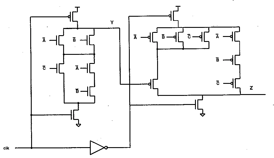
FN12-10b, p17 (Fall 2012 final, 9 points). In the following circuit, find Z (Boolean equations) as a function of A, B, and C. During what phase of clk (high or low) does Y evaluate? Z evaluate?
Hint
What it asks. Two things: the clock phase in which each stage evaluates, and Z as a Boolean function of A, B and C. The words “During what phase of clk” tell you to read the clocked devices before the logic: the second stage’s devices are on , not clk.
The idea. Use the first two moves of M6’s dynamic-logic approach: find whether each stage is n-type or p-type from its clocked devices, then read each node from its network (an n node is , a p node is ). What is new is NP domino: a p-type stage driven directly by a bare n node, with no inverter between them (Chapter 12, Section 5). That is safe here because the n node rests at 1, and a 1 on a PFET’s gate keeps it off, so the second stage cannot start early. Then Z uses Y as an input, so name what Y means before simplifying Z.
The clock phases
- Stage 1 (node Y). The clocked devices decide the type, so read them first: a PFET on clk above an NFET network, a footer on clk below. clk = 0 precharges Y to 1; clk = 1 evaluates. An n-type stage, evaluating while clk is high.
- Stage 2 (node Z). Its clocked devices are on , so follow the inverter: a PFET on at the top, PFETs doing the logic, an NFET on to ground. clk = 0 makes : the NFET pre-discharges Z to 0 and the top PFET is off. clk = 1 makes : the top PFET conducts and the NFET is off, so the PFET network may pull Z up. A p-type stage, also evaluating while clk is high.
- Why no race. Y rests at 1, which keeps the PFET it drives off, so stage 2 cannot start early. This is Lecture 12’s NP (zipper) domino (Chapter 12, Section 5): no inverter and no race, unlike FN17-2, where a bare n node drives another n stage.
The function
- Y. Stage 1’s NFETs conduct on 1s of their gates, which are , , : the network conducts when , that is, when at least two inputs are 0. An n node is the complement: , the majority (Chapter 11, Section 4).
- Z. PFETs conduct on 0s of their gates. The left branch, in series with the PFET on Y, conducts when ; the right branch, , , in series, when . A p node equals its network’s conduction function (Chapter 12, Section 6): .
- Simplify. Y depends only on how many inputs are 1, so count them. No input at 1 gives Z = 0; one gives and Z = 1; two give and , so Z = 0; three give Z = 1. Z is 1 for an odd number of 1s: .
- Edges. Each dynamic node can move only once per evaluation, so in evaluate Y can only fall and Z only rise. The inputs , , come straight from outside, so they must be settled before clk rises, as for any dynamic stage.
Check. A full adder must satisfy Z + 2Y = A + B + C, the number of inputs at 1, in binary. Zero ones: 0 + 0 = 0. One: 1 + 0 = 1. Two: 0 + 2 = 2. Three: 1 + 2 = 3. ✓ All eight rows pass.
Answer: Y and Z both evaluate while clk is high. and : a full adder’s carry and sum, built as NP domino. It is the mirror image of MT24-5’s full adder, whose first stage is the p-type one (M6, Section 1).
Remember. Read the clocked devices before the logic: a p stage whose devices sit on evaluates in the same phase as the n stage on clk. A bare n node may drive a p stage directly on the same clock (NP domino); driving another n stage, it races (FN17-2).
The answer key agrees
It leaves Z unsimplified, as ; it is .
Check yourself In FN12-10b, suppose the second stage's top PFET and bottom NFET were wired to clk instead of clk̄. When would each stage evaluate, and what would go wrong?
Stage 2 would evaluate while clk is low, when stage 1 is precharging: its input Y would be held at 1 then (the Y PFET off), and stage 1’s result would arrive only while stage 2 is pre-discharging. Stage 2 would never see the evaluated Y. NP domino needs the p stage’s devices on clk̄ (Chapter 12, Section 5), so that both stages evaluate in the same phase.
5. FN12-10c: a differential gate
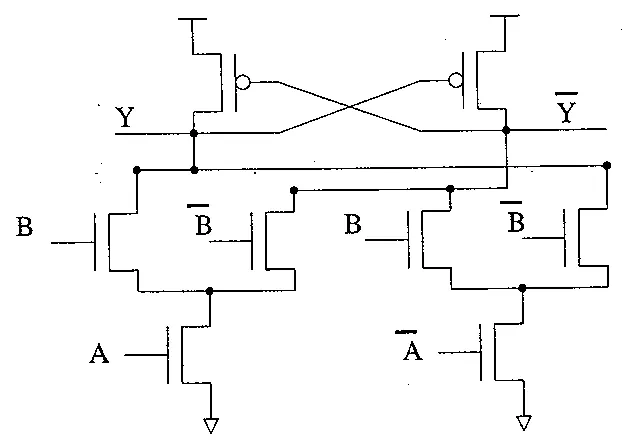
FN12-10c, p18 (Fall 2012 final, 9 points). In the following circuit, find Y and as a function of A and B.
Hint
What it asks. The Boolean function at each of the two outputs, Y and , as functions of A and B. The circuit has no clock, so it is read in its settled states.
The idea. Read it with M5’s pass-transistor approach: node by node, then the function, then what the PFETs from do (move 5). What is new is that the gate is differential. Each output has its own NFET tree to ground, a B or device on top of a foot gated by A or , and the two trees conduct for complementary inputs. Nothing pulls an output up but a PFET gated by the other output: two cross-coupled half latches (Chapter 10, Section 6), as in MT24-3’s carry. So find when each output is pulled down; the PFETs then make the other one high.
Y and Ȳ
- Y’s pull-down. Series devices are AND and parallel paths OR, so follow each path from Y to ground. Through the left B device and the A foot: . Through the right device and the foot: . So Y is pulled down when .
- Ȳ’s pull-down, the same way. Left with A: ; right B with : . Ȳ is pulled down when .
- Compare the two, because a differential gate needs exactly one output low. The two conditions are complements: exactly one output is pulled down for every input.
- The PFETs. Only they can raise an output, and each is gated by the other output. When Ȳ is pulled to 0, it turns on Y’s PFET, which pulls Y to ; Y = 1 keeps Ȳ’s PFET off. These are cross-coupled half latches (Chapter 10, Section 6), as in MT24-3 and HW4-3c.
- Read the outputs. An output is 1 exactly when it is not pulled down, so , and , the XNOR.
Check. Trace one row through the transistors, without the algebra. A = B = 1: the A foot is on, and the left B device above it connects Y to ground, so Y = 0. Ȳ’s paths need (left) or the foot (right), both off, so Ȳ is not pulled down, and Y = 0 turns on Ȳ’s PFET: Ȳ = 1. And . ✓
Answer: and .
Remember. In a differential gate each output has its own NFET tree, the two trees conduct for complementary inputs, and cross-coupled PFETs lift whichever output is not pulled down. Read the function from the pull-downs: an output is 1 when its tree is off.
The answer key agrees
Is it static? Not asked, but it is the question the midterms ask of every such circuit. Each output has exactly one path to a rail in every settled state, but when the inputs change, the output that must fall still has its PFET on (its gate is the other output, still 0), and the NFETs must overpower it. Correct operation depends on the PFETs being weaker: ratioed by Lecture 10’s test (Chapter 10, Section 9), the verdict of M5 for MT24-3a and of H4 for HW4-3c. The style is often called differential cascode voltage switch logic; the lectures never use that name, and nothing here depends on it.
Check yourself In FN12-10c, how many transistors does each output's evaluation pass through, and why does the gate need both A and Ā but no inverter of its own?
Two in series: one B or B̄ device and one foot (A or Ā). The gate takes both polarities of each input and makes both polarities of its output, so a chain of such gates never needs an inverter: each one passes its Y and Ȳ to the next, which uses them as its A and Ā. (Compare domino logic, which carries true and complement signals for the same reason, Chapter 11, Section 6.)
6. FN10-7: a pass-transistor network that counts
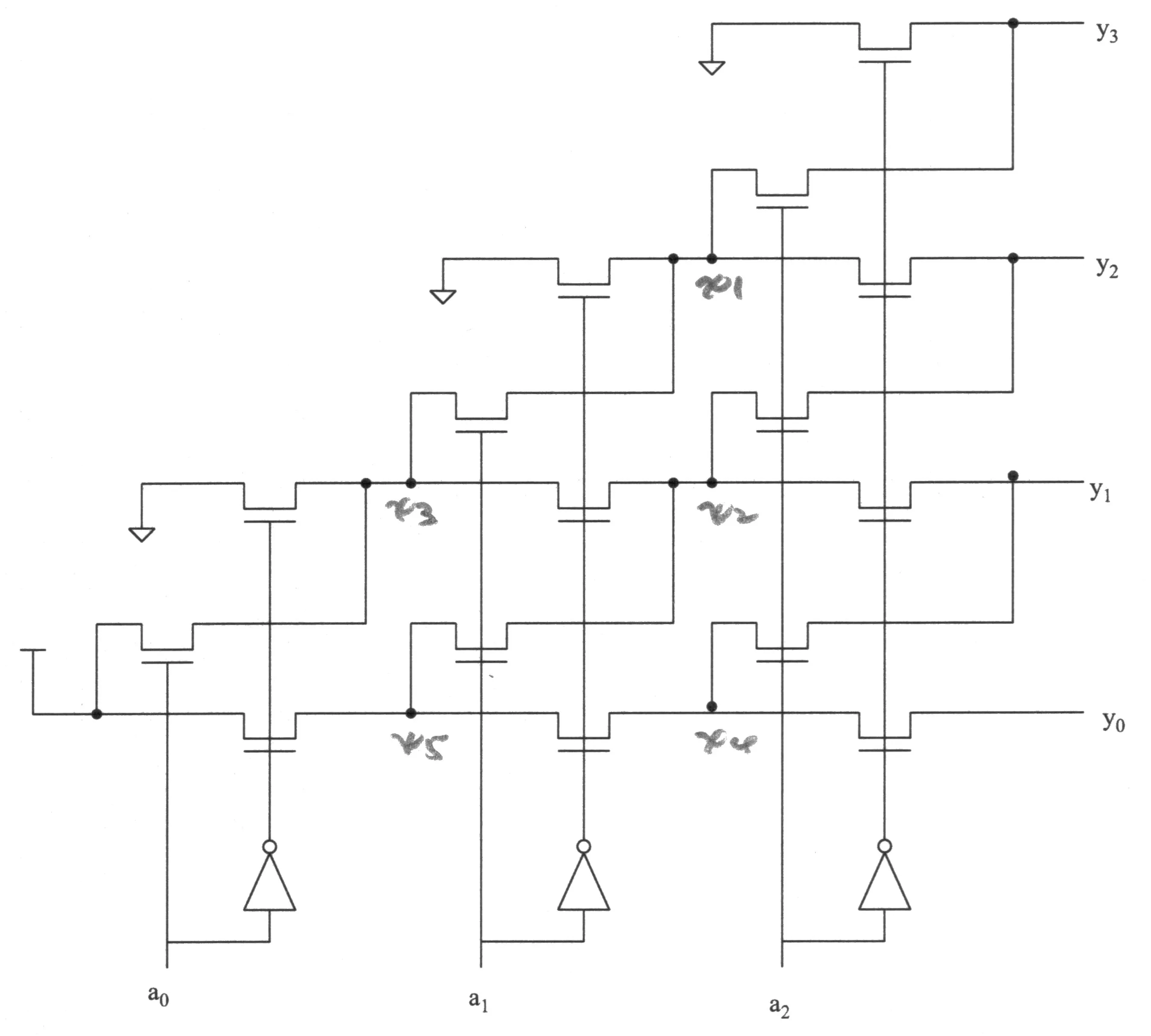
FN10-7, p11–12 (Fall 2010 final, 20 points). Consider the pass transistor network shown above, which computes a four-bit output from a three-bit input . (a) What logic function does this network perform? (10 points) (b) Construct a static CMOS network that performs the same function. (10 points)
FN10-7a: the function
Hint
What it asks. The logic function the network computes: each output – as a function of , , . For 10 points a good answer also says what the function is (its name or its pattern), and whether the network as drawn really computes it.
The idea. Read it with M5’s pass-transistor approach: node by node, then the function, then “static?” and the levels. Each node fed by two devices gated by and is a two-way switch, “if then this input, else that one” (Chapter 10, Section 4). What is new is twofold. The network is a grid that moves one 1 up a row per input that is 1, so its function is a count. And three nodes, , and , have one device each: when that device is off, the node is connected to nothing and floats. That is MT21-1a’s “no select on” case (M5), hidden inside a larger network, so the “static?” move decides the answer here even though the question doesn’t ask it.
Trace it column by column
- Column a0. Start where enters, because every 1 in the network comes from there. M1 (gate ) connects to ; M2 () connects ground to ; M3 () connects to . So always, and when . When , nothing drives .
- Column a1. Each node here picks between two nodes of column a0, so substitute them. is (through ) or ground (through ): . is (through ) or (through ). is through , and nothing when .
- Column a2. Each output again picks between two nodes of column a1, so substitute them: is or ground; is or ; is or ; is through , and nothing when .
- What it does. Name the pattern, because the equations are easier to write and to trust once you know what they should say. A single 1, from , enters at the bottom row. Each column moves it up one row when its input is 1 and leaves it in place when its input is 0; ground fills the top row of each column. So the 1 ends in row , where is the number of inputs that are 1: exactly when of are 1.
- Written out, since the question asks for the function: ; ; ; .
But check every node, as for a multiplexer
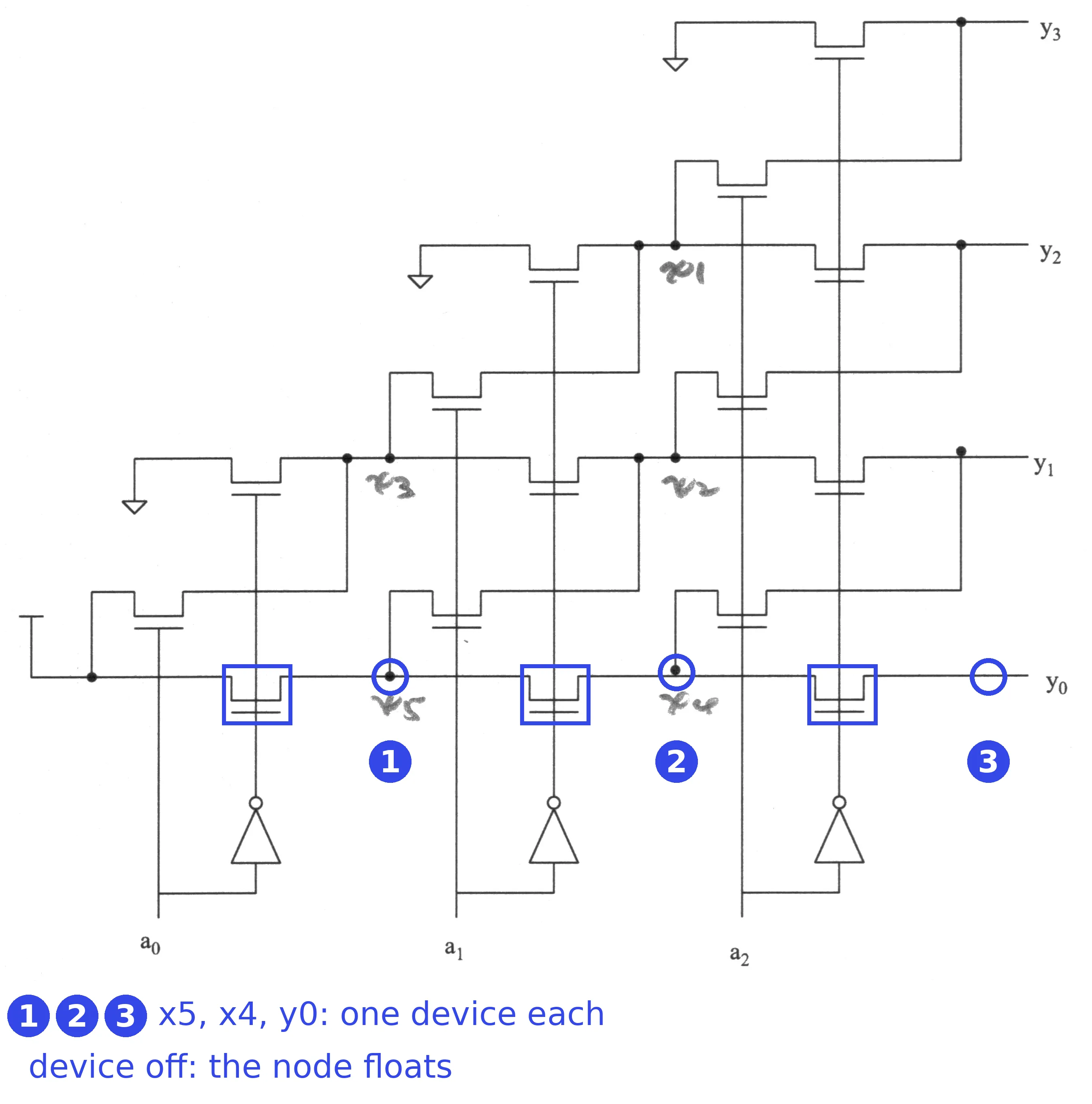
- Count the devices on each node, because a node is static only if it has a path to a rail for every input. Each pair of devices on a node, gated by and , is a two-input multiplexer with one-hot selects: static, one path to a rail (Chapter 10, Section 7). But , and each have only one device (the figure above). When it is off, the node connects to nothing and floats: the “no select on” case of a multiplexer (MT21-1a).
- Floating spreads upward, because a node whose only conducting path leads to a floating node floats too: for and , is connected only to the floating .
- Run all eight inputs, because which nodes float depends on the input (the widget below). The output that should be 1 is always driven high, and the outputs above it are always driven to 0, but every output below it floats. For 011, for example, is driven high, low, and and float.
- Why it matters. A floating node keeps its last value. Go from 000 ( driven high) to 001: is left floating at its old high, so and both read 1. As drawn, the network can give a wrong answer.
- The fix. Each one-device node is a multiplexer missing its other input, so add it: three more NFETs, from ground to , from ground to , from ground to . Then every node has exactly one path to a rail for every input: static, with 18 NFETs and the three inverters.
- Levels. The function’s 1 is only as good as its voltage, so follow it. The 1 is passed through NFETs whose gates are full-rail inputs, so the high output is , one threshold down however many devices it crosses (Chapter 10, Section 5); the 0s are clean.
Check. A count must give exactly one 1 for every input. The four equations have products, one for each of the 8 input rows, and no row appears twice, because each row has one count. ✓ So for every input exactly one output is meant to be 1, and the other three are meant to be driven to 0; the second list found that the ones below it float.
Answer: the network counts the 1s among its inputs, in one-hot form: when exactly of are 1 (the four equations above). The high output is . As drawn, the outputs below the selected one float rather than being driven to 0, so the network is not static; three more NFETs, one per column to ground, make it static.
Remember. In a pass network, count the devices on every node: a node fed by a single device floats when that device is off, and a floating node keeps its old value, not 0. Recognize a counting grid by a 1 entering one corner and each input moving it one row.
The answer key differs
It gives the same four equations, from , and . Its (and with it and ) treats a node that nothing drives as a 0. The equations describe what the network is meant to compute, but in the circuit as drawn those 0s are floating nodes, which keep whatever they held before.
What to notice.
- As drawn, try 001, 011 and 111: the outputs below the 1 show “float”.
- With the three NFETs added, every row is driven: one output at (4 V at the lecture’s 5 V and 1 V), the others at 0.
FN10-7b: a static CMOS equivalent
Hint
What it asks. A complementary static CMOS circuit (pull-up PFETs, the dual pull-down NFETs) with the same four outputs as the network. Only the function has to match: the count of (a), with every output driven to a full rail.
The idea. Same move as M5’s MT24-3d (move 6 of the approach): one complementary gate computes the complement of its pull-down’s expression (Chapter 7, Section 4). What is different here is that the complements of the inputs are already made, by the network’s own three inverters. A PFET gated by conducts when , so feeding a gate the complements absorbs its inversion: one gate per output, each output a sum of products, with no inverter after it.
One complementary gate per output
- Use the inverters that are there. The gates need both polarities of each input, and the network’s own three inverters (6 transistors) already make the complements.
- One PFET branch per product. A PFET conducts on a 0, so a series branch of PFETs gated by the complements of a product’s literals conducts exactly when that product is 1. Each output is a sum of products: one series branch per product, the branches in parallel, from to the output. The pull-down must conduct exactly when the pull-up doesn’t, so it is the dual: one parallel group per product, the groups in series (Chapter 7, Section 4).
- The single-product outputs. has one product, so one branch: three series PFETs gated by , , , three parallel NFETs gated by the same (a NOR of the complements). : the same on , , , a NOR3. Six transistors each.
- The three-product outputs. and have three products of three literals each: three branches of three PFETs, and three groups of three NFETs. 18 transistors each, three high on both sides.
- Count, because the count is the reason the pass network exists. In all, transistors, against the pass network’s 15 NFETs and 6 inverter transistors (24 with the three NFETs that make it static). That difference is why the pass network was drawn.
Check. Trace one row through the gates. Input 011 (, ) has two 1s, so must be 1. Its product is the branch of PFETs gated by , , : all three gates are 0, so the branch conducts and . ✓ In ‘s gate the PFET on is off and the NFET on is on, so . ✓
Answer: four complementary gates fed by the inputs and their complements: and as three-input NORs (of and of ), and as 18-transistor gates with three-high stacks drawn above; 54 transistors with the inverters. Other answers are fine too: for example, as a NAND3 and an inverter (8 transistors) avoids the three-high PFET stack.
Remember. For a static CMOS sum of products, draw one PFET branch per product, gated by the complements of its literals, and the dual below. When the complements are already available, one gate per output needs no inverter after it.
The answer key agrees
It draws the same four gates. Its third inverter’s output is labelled for , a slip.
Check yourself FN10-7b's y3 gate puts three PFETs in series. Using Chapter 7's stack rule, what is its logical effort per input (Rp = 2Rn), and what is the NAND3 + inverter alternative's first stage?
A NOR3’s PFETs must be 3 × 2W = 6W for the balanced drive and its NFETs W: input against the inverter’s , . The NAND3 has NFETs and PFETs : input , , then an inverter (). For a large load the NAND3 + inverter is faster; for a small one, the single NOR3 saves a stage (Chapter 8).
What this means for the midterm
Where each method comes back.
- Dynamic and domino logic (M6; the moves are in its approach section): MT24-5 (a dynamic full adder, like FN12-10b mirrored), MT23-3 (a p-type domino XOR; its half latch is FN12-5b’s fix for a p node), MT17-3c. The midterms ask for the function, a delay and then sizing or noise. FN17-11 and FN17-2 add what they don’t ask yet: what a footless stage requires of its inputs, and the race and collision between two stages. 15–20 minutes for a 30–50 point question.
- Charge sharing and the half latch (FN12-5): MT23-3c–d asks the noise half of the same story (the skewed inverter’s margin, and one transistor to protect the node). About 5 minutes for the number and the reasoning.
- Pass-transistor networks (M5; the moves are in its approach section): MT24-3 and MT23-2 ask “static?”, the function, the levels and a static CMOS equivalent; MT21-1a is FN10-7’s floating node in its simplest form. FN12-10c is MT24-3’s cross-coupled PFETs on a two-input XOR. About 17 minutes for a whole question.
The traps.
- Calling a pass network static because its pairs are one-hot, without checking every node: a node with one device floats when it is off (FN10-7).
- Treating a floating node as 0 in the equations (FN10-7’s key).
- Reading an n node with an inverter after it as the function: a bare n node is , a p node is (FN12-10b, FN17-2).
- Delayed reset or a footless stage without checking that the inputs are back at 0 when precharge starts (FN17-2b, FN17-11).
- A delay on an edge the circuit cannot make (FN17-2c).
- Charge sharing with no path to ground: the node drops anyway; the fraction lost is , and the internal node stops at (FN12-5a).
What the keys get wrong
Re-solving every part found these disagreements and omissions; all are recorded in this page’s review/decisions.md.
| Part | The key | Here |
|---|---|---|
| FN17-11 | inputs: overlapping pulses that reset before the PFET turns on; nothing on Y | right, but incomplete: a minimum width, glitch-free inputs, no input while the PFET is on; Y is one pulse, the OR of the inputs, whose width the loop sets |
| FN17-2a | 556 ps (1/3 µm rounded to 0.3) | 500 ps (solved on M6) |
| FN17-2b | falls 333 ps after | no timing avoids the collision without inverters; that one makes it certain (M6) |
| FN17-2c | 723 ps from A rising to Y falling | A rising cannot make Y fall; 167 ps after rises, 667 ps after (M6) |
| FN10-7a | , | , , float when their one device is off; outputs below the selected one float, so the network as drawn is not static (three NFETs fix it) |
| FN10-7b | third inverter labelled | it makes (a label slip; the gates are right) |
Every other part (FN12-5a, FN12-5b, FN12-10b, FN12-10c) agrees with its key after re-solving; the key leaves FN12-10b’s Z unsimplified () and calls the babysit devices “keepers”.