15. Dynamic flip-flops and clocking domino
Chapters 13 and 14 built sequential circuits from static latches: a latch holds its bit in a loop of two inverters, two latches make a flip-flop, and two-phase clocks let logic borrow time across a transparent latch. Lecture 14, from 6:48, asks what happens when the loop is taken away and the bit is held as charge on a node instead. The answer is a family of fast, small and fragile circuits. The lecturer calls them historical, “far too risky” for a design today (07:33), but they are the place where every idea about races, dynamic nodes and half latches meets clocking. The lecture then turns to domino logic (Chapters 11 and 12) and asks how to clock it between latches without wasting half of every cycle, and closes with the number facts that the adders of Chapter 16 need.
After this chapter you can:
- read the edge of a master–slave flip-flop from its gate polarities, and say which nodes of a dynamic flip-flop hold the bit in each clock phase;
- estimate how long a dynamic node keeps its value, and turn that into a minimum clock frequency;
- explain why a flip-flop that uses and an inverted has a race, and why the C²MOS (NORA) flip-flop removes it;
- walk a TSPC latch or the TSPC flip-flop through its clock phases, find which nodes are dynamic in each state, and place a half latch that removes the state with two dynamic nodes;
- compare domino between flip-flops, two-phase domino and static two-phase latches for a given split of the logic;
- explain flutter, and when a mid-cycle latch can be dropped;
- read three-bit two’s-complement numbers, negate them, and test an addition for overflow.
Boxes and equations marked board were written or said in the lecture. Parts marked added are explanations, arguments or examples this guide adds. The lecture after 6:48 has no numbers of its own, so every number below is an added example, and every one is recomputed in the page’s test.
Symbols
| Symbol | Meaning | Unit | First appears |
|---|---|---|---|
| , | the clock and its complement (here made by an inverter) | — | §1 |
| D, Q, | a flip-flop’s or latch’s input, output and inverted output | — | §1 |
| TG | transmission gate: an NFET and a PFET in parallel, gates on complementary signals | — | §1 |
| the capacitance of a storage (dynamic) node | fF | §1 | |
| the total leakage current out of (or into) a dynamic node | nA | §1 | |
| , | the droop of a dynamic node; the largest droop the next gate still reads correctly | V | §1 |
| how long a dynamic node keeps its value within (not a flip-flop’s hold time) | ns | §1 | |
| , | the clock period and frequency | ns, MHz or GHz | §1 |
| the delay of the clock inverter: the window in which and are equal | ps | §2 | |
| the delay from D through the master gate, the inverter and the slave gate to the slave’s node | ps | §2 | |
| X, Y | internal nodes of the C²MOS and TSPC circuits (Y is the board’s name in the TSPC latch, §4; X, and both names in the TSPC flip-flop, §6, are added) | — | §3, §4 |
| the supply voltage | V | §3 | |
| , | a flip-flop’s clock-to-Q delay and setup time: together its overhead | ps | §7 |
| the delay of a domino block between flip-flops | ns | §7 | |
| , | the two phases of a two-phase clock: complementary, high in the first half of each cycle | — | §8 |
| , | the logic delays of two consecutive blocks between latches | ns | §8 |
| activity factor: full charge–discharge cycles of a node per clock cycle | — | §9 | |
| , | a node’s switched capacitance; its dynamic power | fF; µW | §9 |
| N, Z, S, S′ | in the flutter and overlap figures: a domino block’s dynamic node, its output, a static gate after it, the same gate fed by a flip-flop | — | §9, §10 |
| Chapter 14’s name for the non-overlap window, both phases low (not used here) | ps | §10 | |
| a deliberate overlap: rises this long before falls | ps | §10 | |
| the evaluate delay of the first domino stage of a block | ps | §10 | |
| the number of bits in a word | — | §11 | |
| in §11 only: the overflow flag (1 when an addition overflows), not a voltage | — | §11 | |
| MSB, LSB | the most and least significant bits | — | §11 |
| , | the carry into the MSB position and the carry out of it | — | §11 |
1. A dynamic flip-flop
You need
The transmission-gate latch (Chapter 13 teaches it, from L12 46:55). Its input passes through a transmission gate to a node X, and an inverter after X gives the output. A second inverter and a second transmission gate feed the output back to X. The input gate conducts while the latch is transparent, and the feedback gate conducts while it holds, so the two gates are driven by opposite clocks. While the latch is transparent the feedback is cut, so writing a new value never has to overpower it. While the latch holds, the loop of two inverters keeps X at a full 0 or 1 for as long as the power is on: the latch is static.
A transmission gate (TG) is an NFET and a PFET in parallel, sharing source and drain, with their gates on complementary signals. It conducts when the NFET’s gate is 1 and the PFET’s gate is 0, and then passes both a 0 and a 1 at full level (Chapter 10). It is off when the NFET’s gate is 0 and the PFET’s gate is 1.
Master–slave (Chapter 13). Two latches in series that are transparent on opposite clock levels make an edge-triggered flip-flop. When the first latch, the master, closes, the second, the slave, opens at the same moment and passes the captured value to Q. So the flip-flop’s active edge is the master’s closing edge. Chapter 13’s flip-flop has its master transparent while clk = 1, so it closes, and Q changes, when clk falls: a negative-edge flip-flop.
A dynamic node (Chapter 13 §4 and §6, which builds the dynamic D latch; Chapter 11 §8 for domino) is a node that nothing drives: every transistor connected to it is off. It keeps its value only as charge, , on its capacitance . The off transistors still conduct a little (subthreshold leakage, Chapter 4), so the charge drains away and the voltage droops. A capacitor’s current and voltage are related by .
The question. A static latch spends two transistors and an inverter on its feedback, and its node carries the extra capacitance of the feedback devices. If the bit can sit on a node’s capacitance for the short time until the next clock edge, why not delete the feedback altogether? The lecture’s answer (07:00–10:28): you get a flip-flop that is “blazingly fast”, and one that a careful designer would no longer use.
Start from the static latch
From a static latch to a dynamic one (added)
- Take Chapter 13’s transmission-gate latch and remove the feedback inverter and the feedback gate. What is left is one transmission gate and one inverter.
- While the gate conducts, the node after it follows D, and the inverter’s output follows : the latch is transparent, as before.
- When the gate turns off, nothing drives the node any more. Its charge holds the last value of D, and the inverter keeps showing it. The node is now a dynamic node, and the latch holds only for as long as that charge lasts.
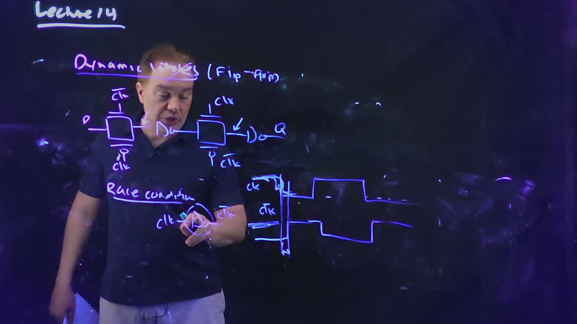
The lecture starts here. Its title is “Dynamic latches (flip-flops)” board: “not a latch” (08:45), because the circuit on the board is two of these latches back to back.
The dynamic flip-flop: two transmission-gate latches with their feedback removed. The master gate (NFET on , PFET on clk) is transparent while clk = 0; the slave gate (NFET on clk, PFET on ) while clk = 1, so D is sampled at clk’s rising edge. The two marked nodes are dynamic: each floats, holding the bit as charge, while its gate is off. The board’s title is “Dynamic latches (flip-flops)”. Lecture14 @ 09:50.
The board (Lecture14 @ 09:50)

Fair copy of the board above (Lecture14 @ 09:50), mark for mark in its own layout. Black is the cyan pen of “Lecture 14” and the blue-violet pen of the rest; neither marks a separate layer, so the copy is all black. The lecturer draws each transmission gate as a square with a gate bar above (the NFET’s clock) and a gate bar with a bubble below (the PFET’s clock); the copy keeps his symbol. “(Flip” and the slave gate’s “clk” are behind the lecturer at 09:50 and are read from 10:54.
Two of them make a flip-flop
The board draws each transmission gate as a box with one clock on a bar above it (the NFET’s gate) and the other on a bubble below it (the PFET’s gate) board.
Which edge, and where the bit is (board, 09:03–09:52)
- The master gate. Its NFET is driven by and its PFET by clk board. Both are on when clk = 0 (), so the master is transparent while clk = 0.
- The slave gate. Its NFET is driven by clk and its PFET by board. It is transparent while clk = 1.
- While clk = 0, the master’s node follows D and its inverter drives to the slave gate, which is off. The slave’s node holds the previous value, and Q does not move.
- When clk rises, the master gate turns off and its node keeps the value D had at that moment. At the same moment the slave gate turns on and passes that value on: Q becomes D. So the flip-flop samples D at clk’s rising edge: it is positive-edge triggered (09:23–09:31) board.
- The two dynamic nodes (the board’s arrows) are the node after each gate board. The master’s node holds the bit while clk = 1, when its gate is off; the slave’s node holds it while clk = 0 (09:37). In each phase one node is driven and the other floats.
Why this one is positive-edge and Chapter 13’s negative-edge added. The active edge is the master’s closing edge. Chapter 13’s master is transparent while clk = 1 and closes when clk falls. This master is transparent while clk = 0 and closes when clk rises. Read the edge from the master gate’s polarities, not from the drawing’s shape: the two flip-flops look the same.
Fast, and fragile
Why anyone built it: “they are blazingly fast. Because I don’t have any feedback to contend with” (09:52) board. Compared with Chapter 13’s latches, writing never has to overpower a feedback inverter (the ungated latch’s fight), and the storage node does not carry the feedback devices’ capacitance (which the gated latch still does). The node is small and nothing opposes the gate that writes it. The DEC Alpha used dynamic latches in the early 1990s (07:43).
Why nobody uses it now (09:57–10:15) board:
- Leakage. The bit sits on a floating node. “If the latch isn’t visited in a while”, the charge leaks off and the bit is lost.
- Noise. A floating node has nothing to restore it, so coupling from a neighbouring wire can push it past the next inverter’s switching point. Chapter 11’s four noise sources all apply to it.
So today these latches “would be considered far too risky” (07:33). They are still worth knowing, the lecturer says, as a rite of passage (07:53), and because the same problems return in every circuit below.
Leakage sets a minimum clock frequency
“Isn’t visited in a while” can be made a number added. Each storage node floats for half a cycle at a time (the master’s node while clk = 1, the slave’s while clk = 0), so the clock must come back before the node has drooped too far.
How long a dynamic node holds (added)
- The droop. While the node floats, the leakage current drains its capacitance . From with a constant current, , so after a time the node has drooped by .
- The limit. The next inverter still reads the node correctly as long as the droop stays below some (for example a fraction of the distance to its switching threshold, with room left for noise). Set and solve for the time: .
- The clock. At a 50% duty cycle each storage node floats for half a period, . That must not exceed : , so .
Memorize or derive. Derive both; they take three lines. (1) with constant gives . (2) Set : . (3) Each node floats for , so .
What breaks it.
- Leakage is not constant. Subthreshold current grows steeply with temperature and with a lower threshold (Chapter 4), so the hot, fast corner sets the limit.
- Another duty cycle. If the clock is low for a fraction of the period, the slave’s node floats for and the master’s for . The longer of the two sets the limit.
- Noise adds to leakage. A coupled glitch can do in a picosecond what leakage does in a microsecond. The formula covers only the slow drain.
A worked example added. For example, a storage node of with out of it, read correctly while it has drooped by less than (with ).
The slowest clock for the example (added)
- How long the node holds. .
- The longest period. Each node floats for half a period, so .
- The minimum frequency. .
- At speed it is harmless. At 1 GHz a node floats for 0.5 ns and droops by .
So in normal running the leakage does not matter. What it forbids is a slow or stopped clock: testing at low speed, or stopping the clock to save power. A static latch holds through both, and a chip built from dynamic flip-flops loses its state. That is one reason the lecture calls them risky.
Traps.
- Reading the board’s arrows as signal flow. They point at the two storage nodes, not along the data path.
- “Master–slave means negative-edge.” That is true of Chapter 13’s flip-flop only. This master is on for its NFET, so it is transparent while clk = 0, and the flip-flop is positive-edge.
- “Two latches, so it is static.” Nothing restores a node once it has drooped. Static means a feedback loop, and this circuit has none.
- Confusing with a hold time. A flip-flop’s hold time is about how long D must stay put after the edge. here is how long a floating node keeps its charge.
Check yourself In the dynamic flip-flop, which node holds the bit while clk = 1, and which devices does it leak through?
The master’s node, the one after the master gate. While clk = 1 that gate is off (its NFET’s gate , its PFET’s gate clk = 1), and the node is attached only to that gate’s two off devices and the inverter’s input. It leaks through the two off devices of the master gate (subthreshold, toward whatever D is) and through their drain junctions. The inverter’s gate draws essentially nothing.
Check yourself In the worked example, halve Cs to 1 fF and double Ileak to 2 nA. What are thold,max and the minimum clock frequency?
, so and . Both changes act in the same direction, so the minimum frequency goes up by . Scaling does both at once: smaller nodes and leakier devices.
Check yourself Why is this flip-flop faster than Chapter 13's static flip-flops at the same device sizes?
Writing a static latch whose feedback is not gated means overpowering the feedback inverter; gating the feedback removes the fight but leaves the feedback gate’s devices on the storage node. The dynamic flip-flop has neither: the transmission gate charges a node that carries only its own diffusion and the next inverter’s gate, and nothing opposes it.
2. The clock-inverter race
You need
The dynamic flip-flop of Section 1. D passes a master transmission gate to a node, an inverter, a slave transmission gate to a second node, and an inverter to Q. The master gate’s NFET is driven by and its PFET by clk, so it conducts while clk = 0. The slave gate’s NFET is driven by clk and its PFET by , so it conducts while clk = 1. With exact complementary clocks the two gates are never on together, and the flip-flop samples D at clk’s rising edge.
Device conduction. An NFET conducts when its gate is 1, a PFET when its gate is 0. A transmission gate conducts if either of its devices conducts, even when its two gate signals are not complementary.
A race (Chapter 11 §5). A circuit has a race condition when its function depends on which of two delays is faster. Delays move with process, voltage and temperature, so a design that relies on one winning is unsafe. Chapter 11’s race was two cascaded dynamic gates on one clock; the domino inverter removed it.
The question. The flip-flop needs clk and , and the obvious way to get is an inverter. An inverter has a delay. What happens to the flip-flop during that delay?
clk̄ comes from an inverter
The two clocks are not complementary (board, 10:28–11:25)
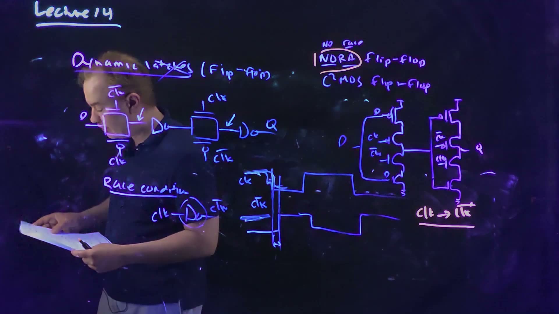
- is late. An inverter driven by clk makes : the same waveform, inverted and delayed by the inverter’s delay (10:28–10:47) board.
- After clk falls, is still 0 until the inverter has switched. For both clocks are 0 (11:15–11:25) board. The board marks this window.
- After clk rises, is likewise still 1 for : both clocks are 1 added. The board marks only the first window; the second follows from the same delay.
made by an inverter is late by the inverter’s delay , so the two clocks are not complementary for after each clk edge. After clk falls both are 0 (the window the board marks): both transmission gates’ PFETs conduct and D can flush through to Q half a cycle early. After clk rises both are 1 (dashed, added): both NFETs conduct, which makes a hold time. A sketch: no times are stated. Lecture14 @ 11:56.
The board (Lecture14 @ 11:56)
Fair copy of the board above (Lecture14 @ 11:56), mark for mark in its own layout. Black is the cyan pen of “Lecture 14” and the blue-violet pen of the rest; neither marks a separate layer, so the copy is all black. The flip-flop and the title are as at 09:50, and the clock row is labelled “ck” on the board. The waveforms are copied as they stand after the redraw: at 10:54 clk̄ was first drawn in phase with clk, and at 11:02 the lecturer erased it and drew it inverted. The wiped first start of clk̄ is left as a smear above its low start; the copy leaves the smear out. The circled inverter is behind the lecturer’s hand at 11:56; its body and output are read from 12:41.
Both clocks low: the data flushes through
The flush (board, 11:25–11:46)
- In the window clk = = 0, look at every PFET, since a PFET conducts with its gate at 0. The master gate’s PFET has its gate on clk = 0: on. That is correct, because the master is opening.
- The slave gate’s PFET has its gate on , which is still 0: also on board. The slave should already be closed, but it conducts through its PFET.
- Both gates conduct at once. For there is a path from D through the master gate, the inverter and the slave gate to the slave’s node: the flip-flop is briefly transparent from end to end. New data at D can “flush through” to Q (11:25–11:46) board.
- What goes wrong. Q should change only at the rising edge. Here a new D, launched for the next cycle, can reach Q at the falling edge, half a cycle early.
The dynamic flip-flop in the window just after clk falls, when the late is still 0: every gate sees 0. Both NFETs are off (dashed) but both PFETs are on, so for the master and the slave conduct at once and a new D can run through to the slave’s node, a path of delay (arrow). The flip-flop is safe only if added. Added; the lecture describes it at Lecture14 @ 11:25–11:46.
Both clocks high: the mirror window
Both gates also conduct at the other edge, through the NFETs added. Just after clk rises, is still 1. The master gate’s NFET (gate ) is still on, though the master should be closing, and the slave gate’s NFET (gate clk = 1) is on, as it should be. So the master really closes only when falls, after the edge. A D that changes in that time runs through both gates and replaces the value the flip-flop was supposed to capture. Here the slave is meant to be open, so the damage is not a value arriving half a cycle early. It is a hold requirement set by the clock inverter: D must stay put for about after each rising edge.
The race condition
“A race condition is defined as whether the functionality of the circuit depends on two relative delays” (12:05) board. Here the two delays are the clock inverter’s and the time the data needs to get through, : from D through the master gate, the inverter and the slave gate to the slave’s node.
Memorize or derive. Memorize the definition of a race (board). Derive the condition: after clk falls, both gates conduct for ; the data at D starts through the master gate at the window’s start and reaches the slave’s node after ; so the slave closes in time only if .
A worked example added. For example, the clock inverter has ; the master gate takes 10 ps, the inverter 12 ps and the slave gate 10 ps.
Is the flip-flop safe? (added)
- The flush path. .
- The comparison. : safe, by 17 ps.
- Load the clock inverter. The clock wire that drives many flip-flops makes the inverter slower. With , : the data gets through, 8 ps before the window closes.
The margin is a comparison of two delays that have nothing to do with each other: one is set by the data path’s devices, the other by the clock buffer and its load. They move differently with process, voltage, temperature and wiring. That is the reason the lecture rejects the design: “an inherent race condition” (11:50).
Traps.
- Drawing early. The lecturer drew it the wrong way at first and corrected himself (11:01): “I said the right thing and drew the wrong thing”. The inverted clock is late, so each window comes after a clk edge, never before it.
- Only the falling-edge window. After the rising edge both NFETs conduct for too. There the slave is supposed to be open, so it shows up as a hold time of about , not as an early Q.
- “Make the clock inverter faster.” That shrinks but cannot make it zero, and the race is still a race: the circuit still depends on beating it.
Check yourself Which overlap window lets data through the PFETs of both gates, and which through the NFETs?
After clk falls, clk = clk̄ = 0 for : the master’s PFET (gate clk) and the slave’s PFET (gate ) are both on. After clk rises, both clocks are 1: the master’s NFET (gate ) and the slave’s NFET (gate clk) are both on.
Check yourself With tflush = 32 ps, what is the largest clock-inverter delay that is safe? At a fast corner tflush becomes 20% shorter while tw stays 15 ps. What is the margin now?
Safe needs . At the fast corner , so the margin falls from 17 ps to . The question assumes a corner that speeds up only the data devices, for example because the clock inverter’s delay is set mostly by the long clock wire it drives, which does not get faster. The margin then shrinks: the two delays do not track.
3. The C²MOS (NORA) flip-flop
You need
The race of Section 2. comes from an inverter, so it lags clk by the inverter’s delay . For after clk falls, both clocks are 0; for after clk rises, both are 1. In the dynamic flip-flop each window turns on one device of both transmission gates (the PFETs after the falling edge, the NFETs after the rising edge), so D can run through the master and the slave together.
An inverting CMOS stage. Its output is pulled up through PFETs, which conduct when their gates are 0, and down through NFETs, which conduct when their gates are 1. A device in series with a stage’s network can switch that network off. If both networks are off, the output floats and keeps its charge.
Positive-edge master–slave (Section 1). The master is transparent while clk = 0 and the slave while clk = 1. The master closes, and the slave opens, when clk rises.
The question. The race comes from two gates that can both pass data when the clocks overlap. Can each latch be built so that, in either window, it can push its output only in one direction, and in a direction that cannot get past the next latch? The lecture’s answer is a flip-flop named for exactly that: “NORA, standing for no race” (12:35), “also sometimes called a C squared MOS flip-flop” (12:42) board. added In the literature NORA is also the name of a dynamic-logic style built around latches like these; here it means this flip-flop.
The circuit: two clocked inverters
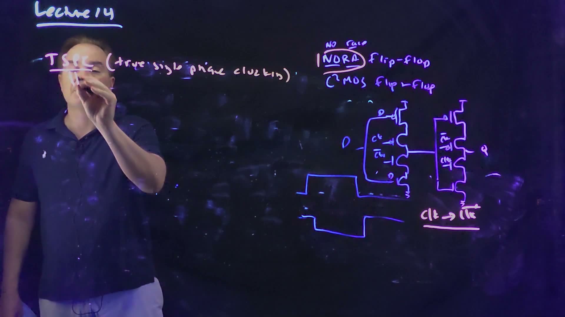
The C²MOS flip-flop (board, 12:53–15:05)
- The master is a stack of four devices between and ground, top to bottom: a PFET with gate D, a PFET with gate clk, an NFET with gate , an NFET with gate D board. Its output X (this guide’s name) is the node between the two clocked devices.
- While clk = 0, both clocked devices are on (the PFET’s gate clk = 0, the NFET’s gate ), and the stack is an inverter: X = . While clk = 1 both clocked devices are off, and X floats with its value. This is a clocked inverter: a transparent-low latch, with X as its dynamic node. (“C²MOS” is clocked CMOS.)
- The slave is the same stack with the clocks swapped, driven by X: a PFET with gate X, a PFET with gate , an NFET with gate clk, an NFET with gate X board. Its output is Q. It inverts while clk = 1 (Q = ) and floats while clk = 0.
- Together they make a positive-edge flip-flop, like Section 1’s: the master follows D while clk = 0, holds when clk rises, and the slave then shows at Q.
The C²MOS (NORA, “no race”) flip-flop: two clocked inverters. The master’s clocked devices, a PFET on clk and an NFET on , make it invert while clk = 0 and float while clk = 1; the slave has the clocks swapped. X (this guide’s name) is the master’s output. Lecture14 @ 15:05.
The board (Lecture14 @ 15:05)
Fair copy of the board above (Lecture14 @ 15:05), mark for mark in its own layout. Black is the blue-violet pen of the board and the cyan of “Lecture 14”; magenta is a pink pen, used for the circle round “NORA” and the stroke left of it, and for “clk → clk̄” with its underline. The left half is unchanged since 11:56. The master gate is behind the lecturer at 15:05 and is read from 14:33. The lecturer draws each stack as one wire with a bump for each channel and a gate bar beside it; the copy draws them as MOSFETs, with a bubble on each PFET gate.
Why the overlap windows cannot pass data
The lecturer leaves the argument to the reader: “I’ll let you go through that” (13:35). Here it is, one window at a time added.
The both-low window after clk falls (added)
- Which devices are on. With clk = = 0, every clocked NFET is off: the master’s (gate ) and the slave’s (gate clk). Every clocked PFET is on: the master’s (gate clk) and the slave’s (gate ).
- So each stage can only pull up. The master can raise X (if D = 0) but cannot lower it. The slave can raise Q (if X = 0) but cannot lower it.
- A new D cannot get through. For new data to reach Q, X must change and Q must answer it. X can only rise. But X rising turns off the slave’s PFET with gate X, the only way the slave could move Q. And X cannot fall, which is the only change that would switch the slave’s pull-up on.
- So Q keeps its value until rises and the window ends. By then the slave’s clocked PFET is off, and the slave is properly closed.
The both-high window after clk rises (added)
- Which devices are on. With clk = = 1, the clocked PFETs are off and the clocked NFETs are on. Each stage can only pull down.
- The mirror argument. The master can lower X (if D = 1); X falling turns off the slave’s NFET with gate X, its only way to lower Q. And X cannot rise. So nothing passes to Q inside the window.
- No race is not no hold time. The master’s pull-down stays on until falls. A D that rises within of the edge still pulls X down, and the slave shows it once the window ends. So, as in Section 2, D must stay put for about after the rising edge. What C²MOS removes is the path from D to Q through both latches at once.
Why C²MOS has no race. (a) Just after clk falls, both clocks are 0: every clocked NFET is off (dashed) and every clocked PFET on, so each stage can only pull its output up (arrows). X rising turns off the slave’s PFET with gate X, so no new value passes both stages. (b) Just after clk rises, both clocks are 1: the mirror, each stage can only pull down. Added argument; sharp clock edges assumed.
Memorize or derive. Derive it in three lines when asked “why is there no race”: (1) in the both-0 window only the clocked PFETs are on, so both stages can only pull up; (2) X rising turns the slave’s pull-up off, and X cannot fall; (3) so Q cannot change until the window ends, and the both-1 window is the mirror.
A worked example: a state walk added.
New data in the both-low window (added)
- Before the falling edge. At the last rising edge D was 0, so the master holds X = 1 and the slave shows Q = 0.
- clk falls, and D = 1 arrives at once, inside the window. The master’s pull-down needs : off. Its pull-up needs D = 0: off. X stays at 1, floating.
- The slave. Its pull-up needs X = 0: off. Its pull-down needs clk = 1: off. Q stays at 0.
- Compare Section 1’s flip-flop. There both PFETs would conduct, and D = 1 would reach Q half a cycle early. Here nothing moves until rises; then the master inverts again (X falls to 0) while the slave is closed.
That walk is the easy case: nothing could move. The case that exercises the argument is the other data value.
New data that does move X (added)
- Before the falling edge. At the last rising edge D was 1, so X = 0 and Q = 1.
- clk falls, and D = 0 arrives at once. The master’s pull-up (PFET with gate D, PFET with gate clk) now conducts, so X rises to 1 inside the window.
- The slave. X rising turns off its PFET with gate X, and its pull-down needs clk = 1: off. Q stays at 1, floating. The master’s change has disabled the only device that could have passed it on.
- After the window the slave is closed by its clocked PFET, and Q keeps 1 until the next rising edge, as it should.
The caveat, and what is still missing
A slowly slewing clock (14:21–14:39) board. “No race” assumes sharp edges. If clk and change slowly, both sit near mid-rail together for a while. added Then every clocked device is partly on, each stage is a weak inverter instead of a one-way switch, and a change at D can leak through both stages. The one-way argument needs the clocked devices to be really off.
It still needs board. The board’s underlined “clk → ” (14:12) is the overhead left: every flip-flop still needs a complementary clock, generated and wired to it. Section 4 removes it.
Traps.
- “No race” for any clock. Only for sharp clock edges; a slow edge reopens it.
- Mistaking a clocked inverter for an inverter followed by a transmission gate. In C²MOS the clocked devices sit inside the stack, in series with the data devices. A stage whose clocked PFET is on but clocked NFET off can only pull up; a transmission gate passes both ways.
- “C²MOS needs only one clock.” It needs clk and on every stage. The single-clock circuit is TSPC.
Check yourself In the both-high window after clk rises, which of the slave's devices could move Q, and in which direction? What would have to happen at X for Q to move?
With clk = clk̄ = 1, the slave’s clocked PFET (gate clk̄) is off and its clocked NFET (gate clk) is on. Q can only be pulled down, through that NFET and the NFET with gate X, which needs X = 1. The master in that window can only pull X down, so X can never newly become 1, and Q cannot fall because of new data.
Check yourself Why does a slowly slewing clock reopen the race? Name the devices that are partly on in each stage.
When the edges are slow, clk and clk̄ both spend time near . In the master, the PFET with gate clk and the NFET with gate clk̄ are both partly on; in the slave, the PFET with gate clk̄ and the NFET with gate clk. Each stage then has both networks able to conduct, so it acts as a (weak) inverter in both directions. A change at D can move X, and the changed X can move Q, inside the same slow transition: the one-way property is gone.
4. The TSPC latch and its dynamic nodes
You need
The clocked stage of C²MOS (Section 3). A clocked device in series inside an inverting stage switches that stage on and off: while it is on, the stage inverts; while it is off, the network it sits in cannot conduct, and if the other network is off too, the output floats.
A transparent-high latch (Chapter 13 teaches latches). While clk = 1 its output follows D; while clk = 0 it holds the value D had when clk fell, its closing edge.
A dynamic node (Chapter 11). A node is dynamic when neither its pull-up nor its pull-down conducts, so it holds its value as charge alone. Leakage drains it (Section 1) and noise can flip it.
The question. C²MOS still needs at every flip-flop. Can a latch be built with one clock wire and nothing else? Yes: TSPC, true single-phase clocking (14:50–15:06) board, used on the DEC Alpha “circa 1992” (16:08). The lecture builds its latches first and then counts, state by state, which nodes are dynamic.
The board (Lecture14 @ 16:11)
Fair copy of the board above (Lecture14 @ 16:11), mark for mark in its own layout. Black is the blue-violet pen of the NORA board and the cyan of “Lecture 14”; magenta is the pink pen, as at 15:05: here the new heading “TSPC (true single phase clocking)” with its underline, and on the NORA board the circle and “clk → clk̄”. The left half has been wiped, leaving the right ends of the two waveforms. The two strokes under TSPC are the start of an arrow the lecturer is drawing at 16:11; they are copied as they stand (the arrow reaches “DEC Alpha ≈ 1992” by 17:15). “SPC” is behind his head at 16:11 and is read from 17:15.
The transparent-high latch
Two clocked stages, one clock (board, 16:30–19:24)
- Stage 1 has three devices: a PFET with gate D from , then, below the output, an NFET with gate clk over an NFET with gate D to ground board. Its output is the internal node Y.
- Stage 2 is the same with Y as its input: a PFET with gate Y, an NFET with gate clk, an NFET with gate Y. Its output is Q board.
- clk = 1: transparent. Both clocked NFETs are on, so each stage is an ordinary inverter, and D reaches Q through two inversions: Q = D (18:02) board.
- clk = 0: holding. Both clocked NFETs are off, so neither stage can pull its output down. Each can still pull up, through its PFET, if its input is 0.
The TSPC transparent-high latch: two clocked inverting stages on one clock. While clk = 1 both clocked NFETs conduct, each stage inverts, and Q = D. While clk = 0 neither stage can pull down, so each output either is pulled up by its PFET or floats. Y is stage 1’s output. Lecture14 @ 19:24.
The board (Lecture14 @ 19:24)
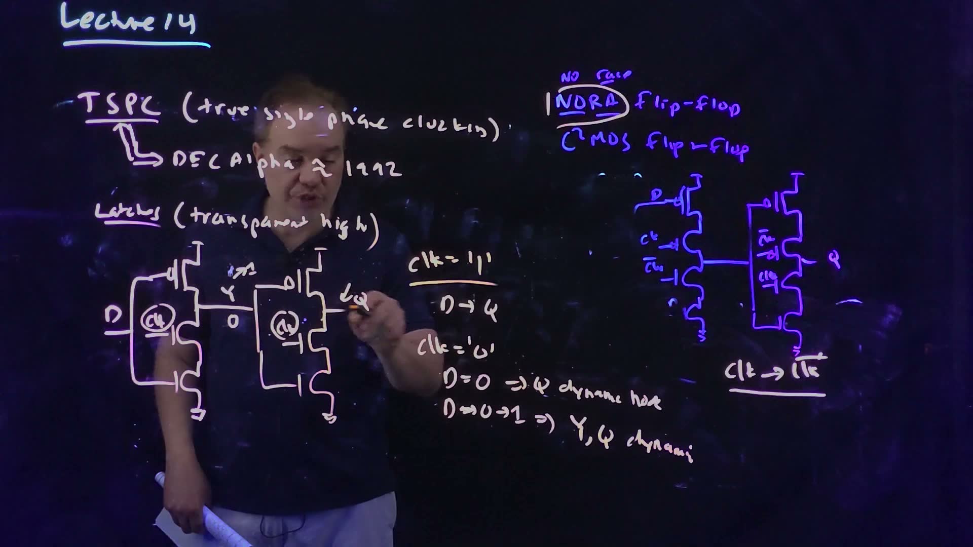
Fair copy of the board above (Lecture14 @ 19:24), mark for mark in its own layout. Magenta is the pink pen, which shows orange while the ink is fresh (the underline of clk = ‘1’): the whole TSPC board, and on the NORA board the circle and “clk → clk̄” as at 15:05. Black is the cyan pen of “Lecture 14” and the blue-violet pen of the NORA board, whose first stack has lost its input loop, its D input and its bottom gate. The lecturer is writing at Q: “Q” stands at 19:24 (read from 18:39, under his pen), “= 1” follows at 19:54 and is not copied. His stacks are drawn as MOSFETs, with a bubble on each PFET gate.
Which nodes are dynamic while clk = 0
While the latch holds, whether a node is driven or floating depends on the data. The lecture lists the cases (board 21:54) board; the table walks each one, with “driven” meaning that one of the node’s networks conducts.
| Case | D when clk fell | D now | Y | Q | Dynamic nodes |
|---|---|---|---|---|---|
| a | 0 | 0 | 1, driven (PFET with gate D on) | 0, floating | Q |
| b | 0 | rose to 1 | 1, floating | 0, floating | Y and Q |
| c | 1 | 1 | 0, floating | 1, driven (PFET with gate Y on) | Y |
Reading the table (board, 18:02–20:23)
- Case a. D = 0, so stage 1’s PFET drives Y to 1. In stage 2, the PFET (gate Y = 1) is off and the clocked NFET is off: Q floats at 0. “Q dynamic node” board.
- Case b. Now D rises while clk = 0. Stage 1’s PFET turns off, and its pull-down is cut by the clocked NFET: Y floats at 1. Q is still floating at 0. “Y, Q dynamic” board.
- Case c. D was 1 when clk fell, so Y was already 0 (it fell while clk = 1). Stage 1’s PFET is off and its pull-down is cut: Y floats at 0. Stage 2’s PFET (gate Y = 0) drives Q to 1. “Y dynamic” board.
- D can still act while the latch holds. It cannot reach Q, but it can switch stage 1’s PFET and so decide whether Y is driven or floating (case b). It can even move Y up: from case c, D falling turns the PFET on and drives Y to 1. Then stage 2’s PFET turns off, Q keeps its 1 as charge, and the bit has moved from Y to Q added.
Why two dynamic nodes are worse
The upset (board, 20:49–21:16)
- The state. Case b: Y floats at 1 and Q floats at 0 (20:49) board.
- A disturbance at Y. Noise or leakage pulls Y down (the board’s “1 → 0”).
- Stage 2 answers. Its PFET has gate Y, so a falling Y turns it on. Q is floating, nothing holds it at 0, and the PFET pulls it up: “Q = 0 → 1” board.
- So the bit can be lost two ways: through a disturbance of Q itself, or through one of Y. In cases a and c only one node can be disturbed.
The upset that makes two dynamic nodes dangerous (case b: D was 0 when clk fell, then rose to 1). With clk = 0 both clocked NFETs are off, and with D = 1 stage 1’s PFET is off too, so Y floats at 1 and Q floats at 0 (open circles). A disturbance that pulls Y down (jagged arrow) turns on stage 2’s PFET, and Q, with nothing holding it, rises: the stored 0 is lost. The devices are drawn in the state after the disturbance (Y = 0). Lecture14 @ 21:09.
The board (Lecture14 @ 21:09)
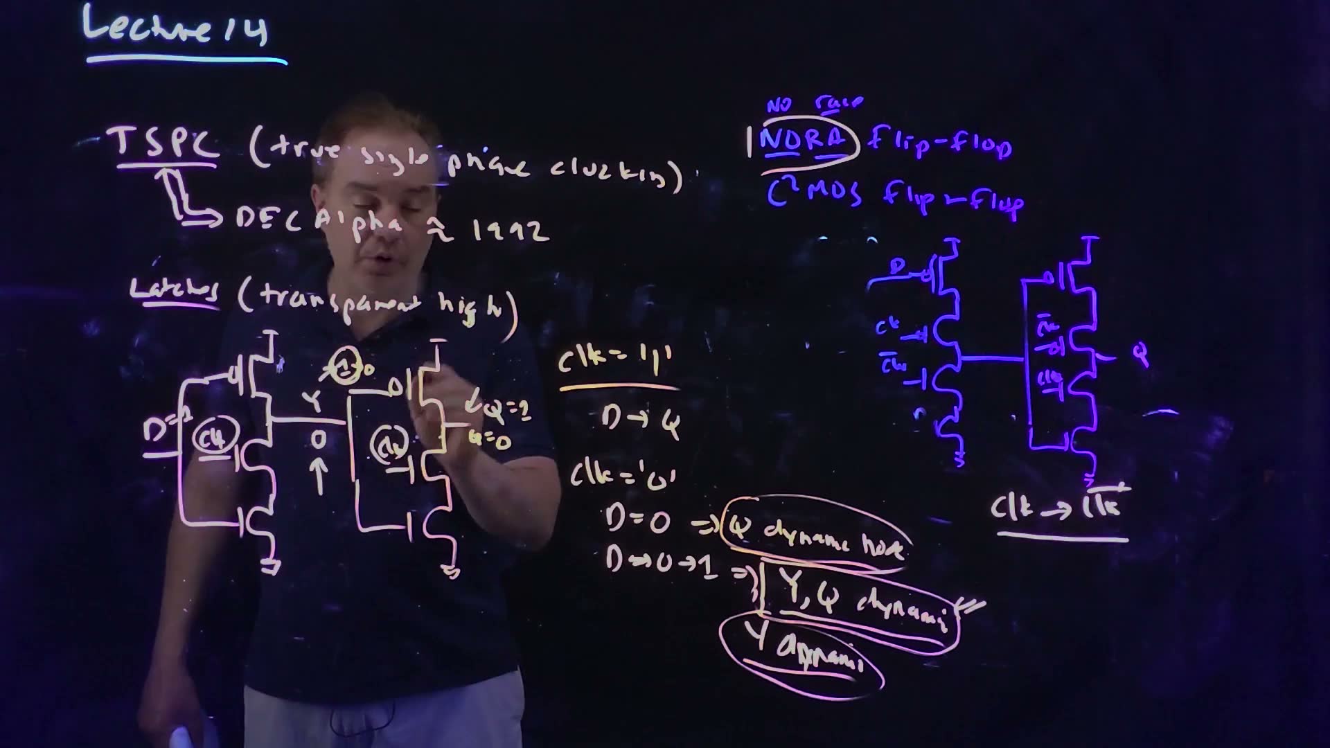
Fair copy of the board above (Lecture14 @ 21:09), mark for mark in its own layout. Magenta is the pink pen (its fresh strokes, “Q = 0” and “= 1” at Q, show orange): the whole TSPC board, and on the NORA board the circle and “clk → clk̄” as at 15:05. Black is the blue-violet pen of the NORA board and the cyan of “Lecture 14”. New since 19:24: “= 1” at D; the 1 above Y circled, with a 0 after it (Y pulled from 1 to 0) and an up arrow under Y’s 0; “= 1” and “Q = 0” at Q; the three cases ringed, the last two under one bracket, with “Y dynamic” added. The two strokes at the right end of “Y, Q dynamic” mark the case the half latch will remove. The ringed words keep the board’s slope. The board’s “dyname” and “dynami” are set as “dynamic”. His stacks are drawn as MOSFETs, with a bubble on each PFET gate.
added Two floating nodes are dangerous only in this combination, where Y holds the value that keeps stage 2’s PFET off while Q is 0. If D toggles 1 → 0 → 1 while clk = 0, Y and Q both float at 1; a disturbed Y would then turn the PFET on and push Q toward the 1 it already holds, which does no harm.
Memorize board: clocked NFETs make a TSPC latch transparent-high; clocked PFETs make it transparent-low (Section 5).
Traps.
- One storage node. The bit can sit on Q, on Y, or on both, depending on the data. “Where is the bit?” has three answers.
- “While clk = 0 D does nothing.” D cannot reach Q, but it decides whether Y is driven, and it can move Y.
- Putting the clock on the PFET for the high latch. A clocked PFET would make the stage hold while clk = 1, the low latch.
Check yourself The latch is in case c (D was 1 when clk fell: Y = 0 floating, Q = 1 driven). D now falls to 0 while clk = 0. What happens to Y, to Q, and to the output?
D falling turns stage 1’s PFET on, so Y is driven to 1. Y = 1 turns stage 2’s PFET off, and its clocked NFET is off, so Q keeps its 1 as charge: Q is now the dynamic node. The output holds 1 throughout; only the node that stores the bit has moved from Y to Q.
Check yourself Which of the three hold cases is the dangerous one, and why is it worse than the other two?
Case b, D = 0 at the closing edge and then a rising D: Y floats at 1 and Q floats at 0. A disturbance at Q flips the output directly, as in case a; but now a disturbance that pulls Y down also flips it, by turning on stage 2’s PFET. Cases a and c each have one floating node and so one way to lose the bit.
5. The half latch: one dynamic node at a time
You need
The TSPC transparent-high latch (Section 4). Stage 1: a PFET with gate D, then an NFET with gate clk over an NFET with gate D; its output is Y. Stage 2: the same with input Y and output Q. While clk = 0 the clocked NFETs are off, so each stage can only pull up. The three hold cases: (a) D = 0 when clk fell: Y = 1 driven, Q = 0 floating; (b) then D rises: Y floats at 1 and Q at 0, both dynamic; (c) D = 1 when clk fell: Y floats at 0, Q = 1 driven. In case b a disturbance that pulls Y down turns on stage 2’s PFET and raises Q.
The half latch (Chapter 11 §8–9). A weak device driven from a gate’s output that holds a dynamic node at its value. On a domino gate it is a PFET from to the dynamic node, its gate on the domino inverter’s output, so it is on while the node is 1. It is sized at about one tenth of the strength of the network that has to overpower it.
The question. Case b is the dangerous one. Can one transistor take that state away without making the latch slow or ratioed everywhere else?
The PFET half latch
Holding Y at 1 (board, 21:16–22:39)
- Add a PFET from to Y, its gate on Q board. The board routes the gate wire from Q back over stage 2 (21:54).
- In case b, Q = 0, so this PFET is on and holds Y at 1 (21:45). Y is driven now, not floating; only Q is dynamic. A disturbance at Y would have to fight the half latch.
- Check the other cases. In case a, Q = 0 again, the half latch is on, and it agrees with stage 1’s PFET, which also drives Y to 1. In case c, Q = 1, so the half latch is off, and Y floats at 0 as before added.
- What it does not do. Q can still be dynamic (cases a and b), and Y can still be dynamic (case c). “It’s still a dynamic latch” (22:19); “let’s not kid ourselves” (22:32) board. One weak device removes the state with two dynamic nodes; it does not make the latch static.
- The cost added. When the latch is written the other way (clk = 1, D = 1, Q = 0 before the write), stage 1 must pull Y down against the half latch until Q rises and turns it off. So the half latch must be weak: about one tenth of the pull-down it fights, as Chapter 11 sizes it.
The half latch: a weak PFET (drawn small) from to Y, its gate driven by Q through a wire over stage 2. When Q = 0 it is on and holds Y at 1, so the state in which Y and Q both float (case b) cannot arise; when Q = 1 it is off. It must be weak, because stage 1 has to pull Y down against it when a 1 is written. Lecture14 @ 21:54.
The board (Lecture14 @ 21:54)
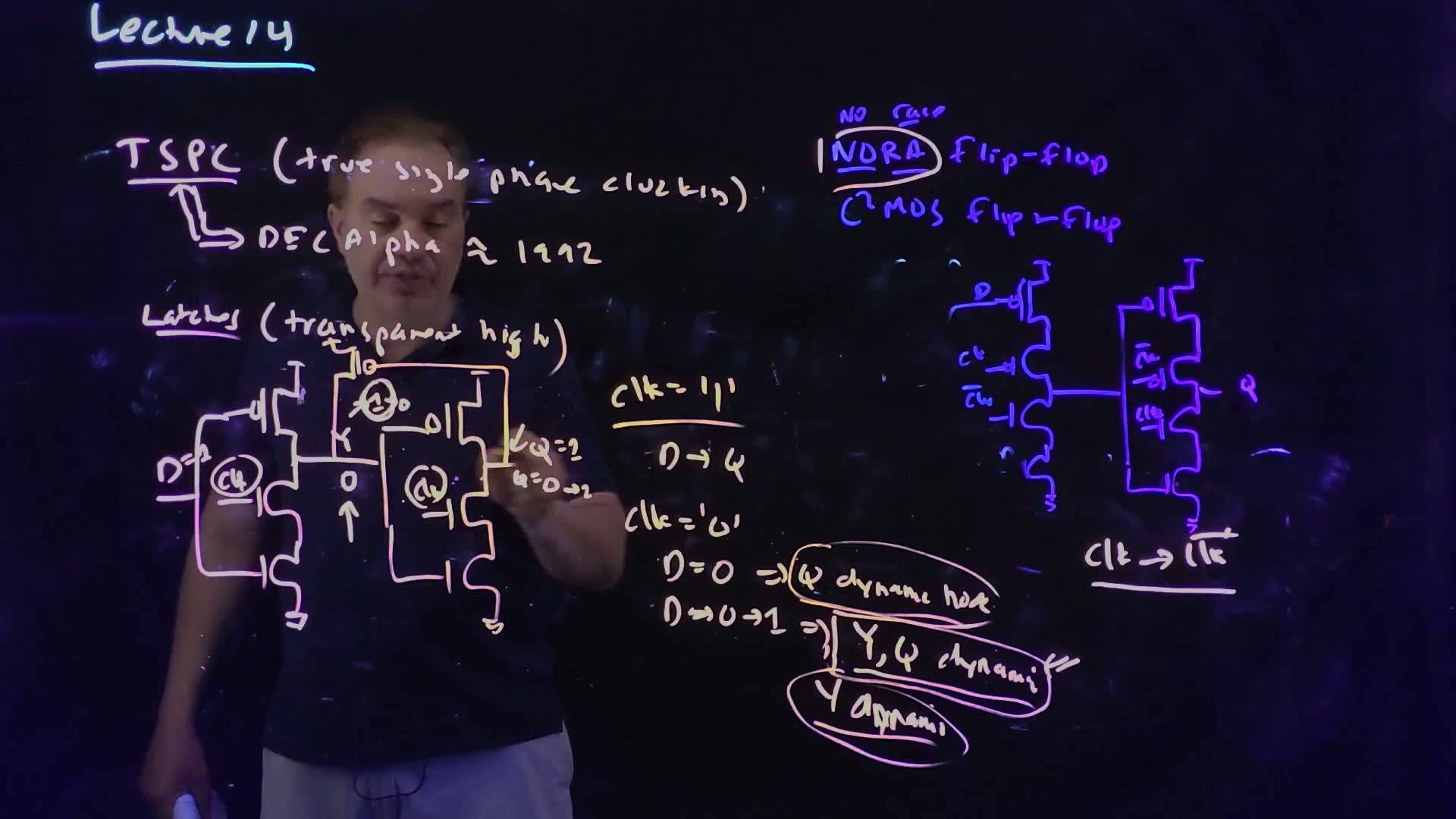
Fair copy of the board above (Lecture14 @ 21:54), mark for mark in its own layout. Magenta is the pink pen (fresh strokes show orange): the whole TSPC board, and on the NORA board the circle and “clk → clk̄” as at 15:05. Black is the blue-violet pen of the NORA board and the cyan of “Lecture 14”. New since 21:09: the half-latch PFET from the supply to Y, its gate wired from Q over the top of stage 2, and “→ 1” after “Q = 0”. “Y, Q dynamic” is not yet struck through; the cross comes later (it stands at 23:32). The ringed words keep the board’s slope; “dyname” and “dynami” are set as “dynamic”. His stacks are drawn as MOSFETs, with a bubble on each PFET gate.
With the half latch fitted, the three hold cases leave one dynamic node each added:
| Case | Y | Q | Dynamic nodes |
|---|---|---|---|
| a: D = 0 when clk fell | 1, driven (stage 1 and the half latch) | 0, floating | Q |
| b: then D rises | 1, held by the half latch | 0, floating | Q |
| c: D = 1 when clk fell | 0, floating (half latch off, Q = 1) | 1, driven | Y |
The transparent-low latch and its NFET half latch
The mirror circuit holds while clk = 1 and passes while clk = 0 board.
The transparent-low latch (board, 22:30–25:17)
- The clocked devices become PFETs. Stage 1: a PFET with gate D, a PFET with gate clk, then an NFET with gate D; Y is between the clocked PFET and the NFET. Stage 2: a PFET with gate Y, a PFET with gate clk, an NFET with gate Y; output Q (24:17) board.
- clk = 0: transparent board. Both clocked PFETs are on, the stages are inverters, and Q = D.
- clk = 1: holding. The clocked PFETs are off, so each stage can only pull down, through its NFET, if its input is 1.
- The dangerous state. D = 1 when clk rose, so Y = 0 (driven by the NFET with gate D) and Q = 1, floating. Then D falls: Y’s NFET turns off and its pull-up is cut by the clocked PFET, so Y floats at 0 and Q at 1 added. A disturbance that lifts Y would turn on stage 2’s NFET and pull Q down. The board marks this state, “0” at Y and “1” at Q (25:17).
- The fix is an NFET. Y must be held at 0, so the half latch is a weak NFET from Y to ground, its gate on Q (24:17) board. In the dangerous state Q = 1, the NFET is on, and Y is held at 0.
The TSPC transparent-low latch, the mirror of the high latch: clocked PFETs, so it passes while clk = 0 and holds while clk = 1, when each stage can only pull down. Its dangerous hold state has Y floating at 0 and Q at 1 (the values shown); a weak NFET from Y to ground, gated by Q, holds Y at 0 in exactly that state. Lecture14 @ 25:17.
The board (Lecture14 @ 25:17)
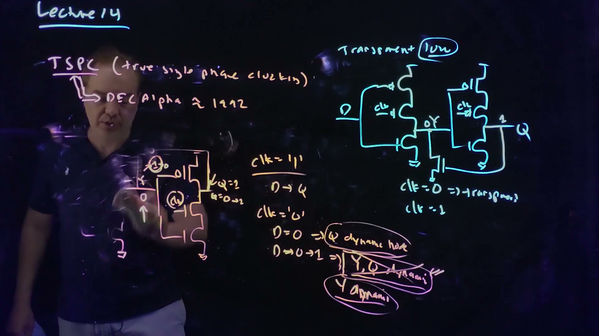
Fair copy of the board above (Lecture14 @ 25:17), mark for mark in its own layout. Black is the cyan pen: “Lecture 14” and the transparent-low latch, drawn where the NORA board was wiped. Magenta is the pink pen: the TSPC board, which the lecturer is wiping at 25:17; only the marks still at full brightness are copied, and the glowing eraser streaks and faint ghosts are left out. “Latches (transparent high)”, D, the input loop, most of stage 1 and the half-latch PFET are gone. “Y, Q dynamic” is now crossed through. The board’s “lvw” is set as “low”, “dyname” and “dynami” as “dynamic”. His stacks are drawn as MOSFETs, with a bubble on each PFET gate; the half-latch NFET is drawn as he drew it.
Memorize the rule and the two pictures. The board shows the two instances (21:54, 24:17); the general statement is this guide’s. To derive it on the exam: find the hold state where Y floats while Q also floats; note Y’s value there; the device that pulls toward that value is a PFET for 1 and an NFET for 0; gate it with Q, whose value in that state turns it on.
Traps.
- “It has feedback, so it is static.” The lecture names this misconception (22:08). The half latch holds Y in one state only; Q is still dynamic in two of the three.
- Putting the PFET half latch on Q. The danger is a disturbance at Y reaching Q through stage 2. The half latch protects Y.
- A PFET half latch on the low latch. Its Y must be held at 0, which only an NFET can do.
Check yourself With the PFET half latch fitted to the transparent-high latch, which node is dynamic in each of the three hold cases?
Case a (D = 0 when clk fell): Q only; Y is driven by stage 1 and the half latch. Case b (then D rises): Q only; the half latch, on because Q = 0, holds Y at 1. Case c (D = 1 when clk fell): Y only; Q = 1 is driven by stage 2’s PFET and turns the half latch off.
Check yourself In the transparent-low latch, which D sequence while clk = 1 leaves Y and Q both dynamic without the half latch, and which device prevents it?
D = 1 at the closing (rising) edge, so Y = 0 and Q = 1; then D falls while clk = 1. Stage 1’s NFET turns off and its clocked PFET is off, so Y floats at 0; Q floats at 1. The weak NFET from Y to ground with its gate on Q (on, since Q = 1) holds Y at 0.
6. The TSPC flip-flop
You need
The two TSPC latches (Sections 4–5). A stage is an inverter with a clocked device in series. Clocked NFETs make a latch transparent while clk = 1 and holding while clk = 0, when its stages can only pull up. Clocked PFETs make it transparent while clk = 0 and holding while clk = 1, when its stages can only pull down. A node is dynamic when neither of its networks conducts. A weak device gated by the output (a half latch) can hold a floating node at its value.
Master–slave (Section 1). A master transparent while clk = 0 followed by a slave transparent while clk = 1 samples D at clk’s rising edge: a positive-edge flip-flop.
Domino precharge and evaluate (Chapter 11 §4). A precharged stage has a clocked PFET from and an NFET network with a clocked NFET at its foot. While clk = 0 it precharges its node to 1; while clk = 1 it evaluates: the node falls if the network conducts, and otherwise floats at 1. In evaluate the node can only fall; once fallen, it stays down until the next precharge.
The question. A positive-edge flip-flop is a transparent-low latch followed by a transparent-high latch: four TSPC stages (24:41–24:58) board. The lecture shows that one stage can go, and that the result is inverting: “data in … Q bar out” (25:03–25:10).
The three stages
The TSPC flip-flop (board, 25:40–27:24)
- Stage 1 is the low latch’s first stage: a PFET with gate D, a PFET with gate clk, an NFET with gate D. Its output is X board. (The board leaves the nodes unnamed; X and Y are this guide’s names.)
- Stage 2 is a precharged stage: a PFET with gate clk from , then an NFET with gate X over an NFET with gate clk to ground. Its output is Y board.
- Stage 3 is the high latch’s second stage: a PFET with gate Y, an NFET with gate clk, an NFET with gate Y. Its output is board. The board writes “Q”, but the flip-flop is inverting (25:10), so this guide labels it .
- The board’s verdict: “pos edge triggered” board. The walk below shows why.
The TSPC flip-flop, “pos edge triggered”: three stages on one clock. Stage 1 (clocked PFET) follows D while clk = 0, giving X = ; stage 2 precharges Y while clk = 0 and evaluates when clk rises; stage 3 (clocked NFET) inverts Y while clk = 1. The output is sampled at the rising edge, so it is labelled here (the board writes Q). X and Y are this guide’s names. Lecture14 @ 27:24.
The board (Lecture14 @ 27:24)
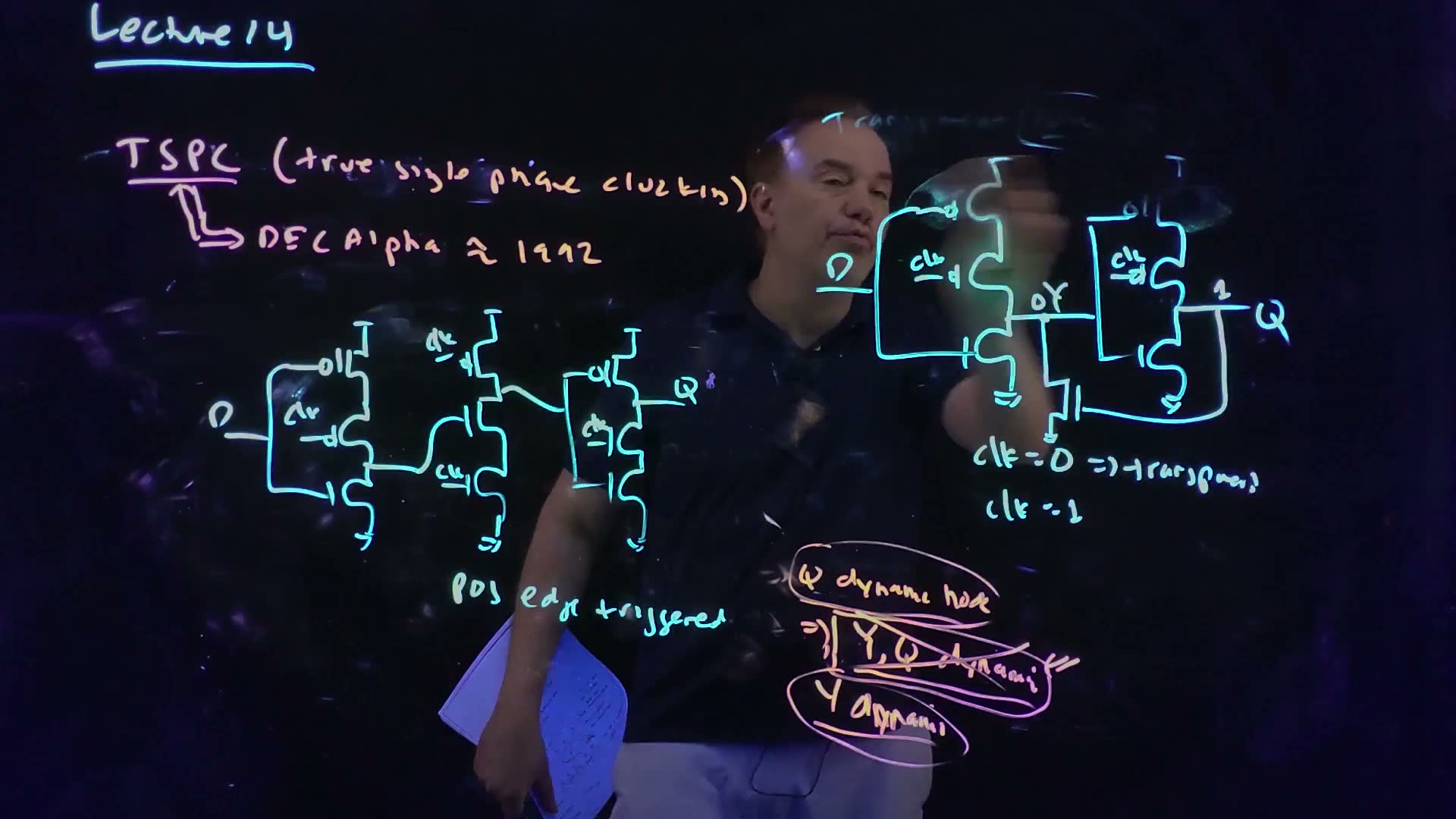
Fair copy of the board above (Lecture14 @ 27:24), mark for mark in its own layout. Black is the cyan pen: “Lecture 14”, the TSPC flip-flop with “pos edge triggered”, and the transparent-low latch. Magenta is the pink pen: the TSPC heading and what is left of the case list. The lecturer is wiping the latch from the top at 27:24; only marks still at full brightness are copied (“Transparent low” keeps only its T, and stage 2 has lost its supply bar and top PFET), and the left half of the case list was wiped by 26:50. † The flip-flop is inverting, so its output is Q̄ (25:02: “you get Q bar out”); the board writes Q. The board’s “dyname” and “dynami” are set as “dynamic”. His stacks are drawn as MOSFETs, with a bubble on each PFET gate.
How it samples on the rising edge
The stage-by-stage walk (added)
- clk = 0. Stage 1’s clocked PFET is on, so stage 1 is an inverter: X = . Stage 2 precharges: Y = 1. Stage 3: its PFET (gate Y = 1) is off and its clocked NFET is off, so floats with its last value.
- clk rises. Stage 2 evaluates: if X = 1 (D was 0), Y discharges to 0; if X = 0 (D was 1), Y stays at 1. Stage 3 is now an inverter: . So D = 0 gives Y = 0 and ; D = 1 gives Y = 1 and . In both cases , sampled at the rising edge.
- clk = 1: why later changes of D do nothing. Stage 1’s clocked PFET is off, so X can fall (if D rises) but cannot rise. Stage 2’s precharge PFET is off, so Y can fall but cannot be raised again. If Y has fallen, it stays down whatever X does. If Y is still 1, then X was 0, and X cannot rise to discharge it. So Y, and with it , is frozen until the next precharge.
- clk falls. Stage 2 precharges and stage 3 floats, so holds. Stage 1 follows D again for the next edge.
Memorize the function: positive-edge, inverting. Derive it from the stages when the circuit is drawn differently: clocked PFET in stage 1 means X follows while clk = 0; stage 2 precharges low-phase and evaluates high-phase; stage 3 inverts while clk = 1.
A worked example: the waveforms
added Let clk be 0 on [0, 2), 1 on [2, 4), 0 on [4, 6), and so on (period 4 units, rising edges at 2, 6 and 10). D is 1 on [0, 5), 0 on [5, 7), 1 on [7, 10.5), 0 on [10.5, 11.5) and 1 from 11.5. starts at 1. Gate delays are ignored.
The TSPC flip-flop’s nodes for the worked example, computed from its stage equations with ideal edges (time units unstated). changes only at clk’s rising edges (dotted), to the complement of D there: D(2) = 1, D(6) = 0, D(10) = 1. D’s rise at 7 and its low pulse on [10.5, 11.5) come while clk = 1 and change nothing. In the shaded interval X floats at 0 and Y at 1: both are dynamic.
Working out X, Y and Q̄ (added)
- X follows while clk = 0, and while clk = 1 can only fall. On [0, 5) D = 1, so X = 0. At 5 (clk = 0) D falls, so X rises to 1. At 6 clk rises with X = 1; at 7 D rises and pulls X down. After that D is 1 at every moment X could rise, so X = 0 from 7 on. On [10.5, 11.5) D = 0 while clk = 1: X cannot rise and floats at 0.
- Y is 1 while clk = 0 and, while clk = 1, falls if X = 1. Edge at 2: X = 0, Y stays 1. Edge at 6: X = 1, Y falls to 0 and stays 0 until the precharge at 8. Edge at 10: X = 0, Y stays 1. So Y = 1 on [0, 6), 0 on [6, 8), 1 from 8.
- is while clk = 1 and holds while clk = 0: 1 on [0, 2), 0 on [2, 6), 1 on [6, 10), 0 from 10.
- The samples. D(2) = 1 gives ; D(6) = 0 gives 1; D(10) = 1 gives 0. The rise of D at 7 and the low pulse on [10.5, 11.5) both come while clk = 1, and change nothing at the output.
- The shaded interval. On [10.5, 11.5) D was 1 at the edge, then fell. X floats at 0 (its pull-up is cut by the clocked PFET) and Y floats at 1 (precharge off, X = 0): both dynamic, the state Check (i) below asks about.
Which nodes are dynamic
added The same bookkeeping as Section 4, for the flip-flop. While clk = 0, X and Y are both driven and only floats. While clk = 1:
| D at the edge | D now | X | Y | Dynamic nodes | |
|---|---|---|---|---|---|
| 0 | 0 | 1, floating | 0, driven | 1 | X |
| 0 | 1 | 0, driven | 0, floating | 1 | Y |
| 1 | 1 | 0, driven | 1, floating | 0 | Y |
| 1 | fell to 0 | 0, floating | 1, floating | 0 | X and Y |
In the last row the bit can be lost two ways: X lifted by noise turns on stage 2’s NFET and discharges Y, or Y drooping turns on stage 3’s PFET. Either raises .
Traps.
- Reading the output as Q. The board writes Q, but the flip-flop is inverting (25:10).
- Expecting X to follow D while clk = 1. It can only fall.
- Hold added. If D rises just after the rising edge while Y is still discharging, X falls and cuts the discharge short, leaving Y at a level in between. D must stay put until stage 2 has evaluated: that is this flip-flop’s hold time.
- Feeding the output back for a counter added. Because , wiring the output straight back to D gives a bit that toggles every cycle. A designer who reads the output as Q and puts an inverter in the loop to make a toggle gets a bit that never changes. (PS5-Q2’s bit 0 needs exactly the toggle.)
Check yourself The lecturer's exercise (27:02): where do half latches go on the TSPC flip-flop? Find the clock phase and data sequence that leave two nodes dynamic, and add one device that removes that state.
While clk = 1, with D = 1 at the edge and then D falling: X floats at 0 and Y floats at 1 (the last row of the table; the shaded interval [10.5, 11.5) of the example). Then . A weak PFET from to Y with its gate on is on exactly then and holds Y at 1, so only X floats. As with the latch’s half latch, it must be weak: when Y must discharge (X = 1 at an edge after a sample of 1, so is still 0), stage 2 has to overpower it until rises and turns it off. The flip-flop is still dynamic: floats throughout clk = 0.
Check yourself The other half of the exercise: build the negative-edge TSPC flip-flop by swapping every stage for its mirror, and say where its half latch goes.
Swap NFETs and PFETs, and and ground. Stage 1: a PFET with gate D over an NFET with gate clk and an NFET with gate D, so X = while clk = 1 and X can only rise while clk = 0. Stage 2 is pre-discharged: an NFET with gate clk to ground, and a PFET with gate clk in series with a PFET with gate X from ; Y = 0 while clk = 1, and while clk = 0 Y rises if X = 0. Stage 3: a PFET with gate clk in series with a PFET with gate Y, over an NFET with gate Y; it inverts while clk = 0 and floats while clk = 1. When clk falls, Y = = D and the output is : negative-edge, still inverting. Its two-dynamic-node state is the mirror: D = 0 at the falling edge, then D rises, leaving X floating at 1 and Y floating at 0. The half latch is a weak NFET from Y to ground, gated by the output (1 then).
Check yourself Why does stage 2 behave like a domino stage, and which of Chapter 11's noise problems applies to it?
It has a clocked PFET that precharges Y while clk = 0, an NFET network (the NFET with gate X) with a clocked footer, and in evaluate Y can only fall. That is a footed dynamic gate. So everything in Chapter 11 §8–12 applies to Y while it floats at 1: leakage through the off NFET, charge sharing, and coupling noise on Y or on its input X. The half latch of Check (i) is Chapter 11’s half latch.
7. Domino between flip-flops
You need
Domino logic (Chapter 11 §4–6). A domino stage is a dynamic gate (a clocked PFET that precharges its node, an NFET network, usually a clocked footer) followed by an inverter. While its clock is 0 it precharges: the dynamic node goes to 1 and the stage’s output, after the inverter, to 0. While its clock is 1 it evaluates: the node falls if the network conducts, and the output rises. A domino output is therefore 0 during every precharge and can only rise during evaluate; whatever it computed is wiped at the next precharge.
Flip-flop timing (Chapter 13 teaches it). Logic between two flip-flops on one clock is launched at one active edge and must arrive before the next, one clock period later. The launching flip-flop’s clock-to-Q delay and the capturing one’s setup time are its overhead, so static logic gets .
The question. The simplest way to use domino in a synchronous design is to put it between flip-flops and clock it with the same clock. What does that cost? “Let’s just be boneheaded about this” (28:19) board.
Half the cycle goes to precharge (board, 28:19–29:43)
- The circuit. A flip-flop, a block of domino logic and a flip-flop, all on clk (28:19–28:47) board.
- The clock’s two halves. “Half the cycle of my clock I’m precharging. The other half of my cycle of my clock I’m evaluating” board.
- Only one half does logic. The domino block can compute only while it evaluates. Its precharge “eat[s] up half of my cycle” (29:19) board, and nothing useful happens then.
- Its result must be caught in time added. The domino’s output exists only until the next precharge resets it to 0, so the capturing element must take it at the end of the evaluate half (a flip-flop on the opposite edge, or one that closes when the evaluate phase ends). Either way the logic gets half a cycle.
- The goal. “Hide the precharge time”: do something useful while each stage precharges (29:43) board. Section 8 does it.
Domino between flip-flops, all on one clock. The domino block evaluates only while clk is high and precharges while it is low, so it gets half of each cycle, , for logic; the other half is precharge, wasted for logic. Lecture14 @ 29:31.
The board (Lecture14 @ 29:31)
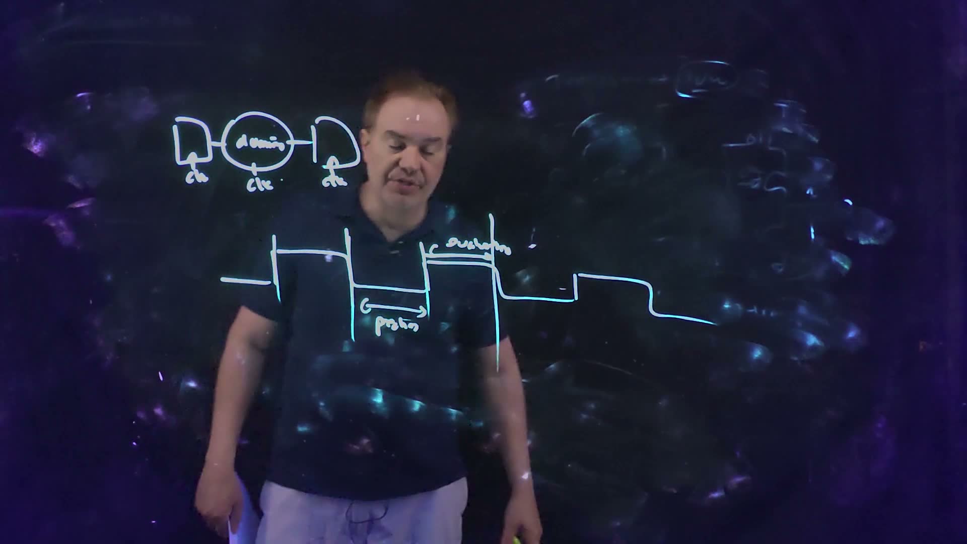
Fair copy of the board above (Lecture14 @ 29:31), mark for mark in its own layout. The board, wiped at 28:17, holds one drawing in one pen (cyan), so the copy is all black. Each arrow starts with a small open hook, as drawn. The board’s scrawled “precharge” and “evaluate” are set in full. The flip-flops keep the lecturer’s D-shaped outline and clock wedge.
Here is the domino block’s delay. Derive it in two lines: the domino can work only in its evaluate phase, which lasts ; subtract the launch and capture overhead as for any flip-flop path.
A worked example added. For example, with overheads ignored. The domino block has 0.5 ns to evaluate; the other 0.5 ns is precharge, wasted for logic. Static logic between the same flip-flops would get the full 1 ns. So the domino logic would have to be twice as fast as the static logic just to break even.
Traps.
- Counting the precharge half as time for logic. The block computes nothing while it precharges.
- “A faster precharge device helps.” The precharge phase lasts as long as the clock is low, however fast the PFET is. A stronger PFET finishes the precharge early and then waits.
Check yourself The clock is changed to a 60% duty cycle (high 60% of the period). With Tcycle = 1 ns and overheads ignored, how long does the domino block get to evaluate, and what must still fit in the rest?
It evaluates while the clock is high: . The precharge must still finish in the remaining . A longer high phase helps the logic only until the precharge no longer fits.
Check yourself Why can't the domino block simply evaluate twice in each cycle?
Every evaluation needs a precharge before it, and with one clock a precharge and an evaluation take one full clock period. Evaluating twice per cycle means a clock twice as fast, which is the same scheme with half the period, still with half of it spent precharging.
8. Two-phase domino
You need
Two-phase clocks (Chapter 14 teaches them). and are complementary: is high in the first half of each cycle and in the second. A latch on is transparent while is high and holds while it is low, and the same for .
Cycle stealing (Chapter 14). Static logic between alternating and latches need not split into exact half-cycles: a block that runs late arrives while the next latch is still transparent and passes straight through, borrowing time from the next block. As long as data arrives at every latch before it closes, two consecutive blocks with delays and need only a clock period .
Section 7’s waste. Domino between flip-flops on one clock spends half of every cycle precharging. Domino precharges while its clock is low and evaluates while it is high; its output is 0 during precharge.
The question. Domino needs a phase in which to precharge. A two-phase clock has two phases. Can each block precharge while the next one evaluates, so that no one waits for a precharge?
Domino on alternate phases
The evaluate wave (board, 29:50–31:40)
- The chain. A latch, a domino block clocked on , a latch, a domino block on , a latch, another domino block, and so on (30:14–30:40) board.
- Each block works on a held value. The block evaluates while is high, which is when the latch in front of it is closed and holding added. The latch behind it is open then, passes the result on, and closes when falls, holding the result while the block precharges.
- The phases swap. “When phi1 is high, this guy is evaluating, this guy is precharging” (31:06) board: the block evaluates while the block precharges, and half a cycle later the roles reverse.
- The precharge is hidden. An “evaluate wave” moves along the chain. Once it has passed into the next block, the block behind it can precharge. “The precharge time is overlapping with the subsequent evaluation, and I don’t see the precharge overhead at all” (31:06–31:40) board.
Two-phase domino. Each domino block (oval) is clocked by the phase opposite to the latch in front of it, so it evaluates while that latch holds its input, and the latch behind it holds the result while the block precharges. When is high the blocks evaluate and the blocks precharge; half a cycle later the roles swap, so the precharge is hidden. P ½ over the block and E ½ over the block are the board’s “precharge ½” and “evaluate ½”. Lecture14 @ 33:07.
The board (Lecture14 @ 33:07)
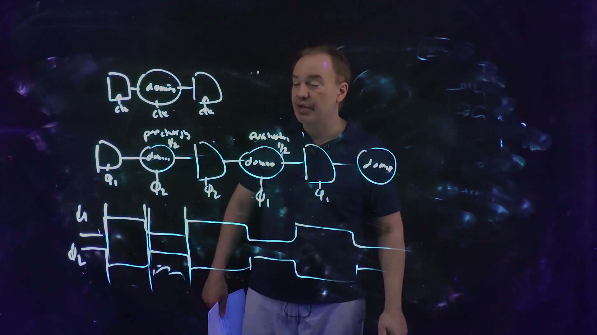
Fair copy of the board above (Lecture14 @ 33:07), mark for mark in its own layout. The board is written in one pen (cyan), so the copy is all black. The top row is the flip-flop, domino and flip-flop of 29:31, unchanged. The scrawled “precharging”, “evaluating” and “domino” are set in full; the latches keep the lecturer’s D-shaped outline. The three long vertical marks through both clocks, and the short strokes between the second and third, were drawn by 31:39 and are copied as they stand.
The evaluate wave (added). Each domino block evaluates (E) while its clock is high and precharges (P) while it is low, so the blocks and the blocks alternate. The result of each evaluation passes (arrows) to the next block, which evaluates in the next half-cycle while the block behind it precharges: no block ever waits for a precharge. Key: P precharge, E evaluate. A sketch, from the lecture at Lecture14 @ 31:06–31:40.
The price: exact half-cycles
What two-phase domino gives up (board, 31:50–33:10)
- No cycle stealing. “All that cycle stealing capability that we had with two phase design with static is basically gone … because this is all clocked now” (31:50–32:21) board. A domino block cannot start before its clock rises, and its result is wiped when its clock falls, so it cannot run into the next half-cycle.
- Less freedom than a flop-based static design. “I have to partition this exactly one half, one half” (32:24–32:36) board. In partitioning, the lecture means: flip-flops need each stage to be one cycle of logic; two-phase domino needs each block to be half a cycle, and the longer half sets the clock. (In speed it still beats domino between flip-flops, Section 7.)
- More phases can recover some of the borrowing, but such schemes “can get to be very, very hairy”, and the lecture does not teach them (32:46–33:10) board.
The same logic, ns and ns, under three clockings, computed from the half-cycle rule. (a) Static two-phase latches: A runs 0.1 ns past the latch in the middle of the cycle (dashed) and borrows it from B, so ns. (b) Two-phase domino at 1.0 ns: A must finish in its half-cycle and overruns it (cross-hatched): it fails. (c) Two-phase domino at ns: each block gets 0.6 ns and B sits idle for 0.2 ns (hatched).
Memorize or derive. Memorize the static-latch bound (Chapter 14). Derive the domino one from the board’s “½, ½”: each block must finish inside its own half-cycle, and , so . The two are equal only for a perfect split, .
A worked example added. For example, 1.0 ns of logic per cycle split and .
Three ways to clock the same logic (added)
- Static two-phase latches. (1 GHz). Block A overruns its half-cycle by and borrows it from block B through the transparent latch.
- Two-phase domino. At 1.0 ns block A would overrun its 0.5 ns half by 0.1 ns, and a clocked block cannot borrow: it fails. Each block must fit its half, so (833 MHz). The period is 20% longer, and block B sits idle for of its half.
- With a perfect split, 0.5 and 0.5 ns, both schemes give 1.0 ns.
- Domino between flip-flops (Section 7). The whole 1.0 ns of logic must fit in one evaluate half: .
So two-phase domino recovers the half-cycle that Section 7 wasted, but only a careful partition makes it as fast as static latches with the same logic, and domino is chosen because its logic is faster to begin with.
Traps.
- Clocking each domino block with the phase of the latch in front of it. The board puts a block after a latch: it evaluates while that latch holds.
- Assuming the static latches’ time borrowing survives. It does not: a clocked block cannot run into the next phase.
- Forgetting the latch after each block. It holds the block’s result while the block precharges. Section 10 shows when one of them can go.
Check yourself For tA = 0.45 ns and tB = 0.7 ns, find the shortest Tcycle for static two-phase latches and for two-phase domino (overheads ignored).
Static latches with cycle stealing: . Two-phase domino: the longer block must fit a half-cycle, so . The uneven split costs domino 0.25 ns per cycle.
Check yourself While φ2 is high, which domino blocks evaluate and which precharge, and which latches are open?
The blocks clocked on evaluate and the blocks precharge. The latches are open (passing the blocks’ results on) and the latches are closed, holding the inputs of the blocks.
9. Domino feeding static logic: flutter
You need
Domino is non-inverting (Chapter 11 §6). Each stage computes an AND–OR function of its inputs, and no network of ANDs and ORs makes an inversion, so domino alone is not logically complete. Its output is 0 in every precharge and can only rise in evaluate.
Dynamic power (Chapter 6 §6). Each full charge and discharge of a node of capacitance draws from the supply. A node that does this once per cycle at frequency dissipates .
A hazard (or glitch) added: a temporary wrong value at a gate’s output while its inputs settle at different times. Each glitch is a full or partial charge and discharge, and costs energy like a real transition.
Two-phase domino (Section 8): latch, domino, latch, domino, and so on.
The question. Domino cannot invert, so real designs follow it with some static logic. Is that free? And which family is lower power in the first place?
Static after domino, and the power of each (board, 33:46–37:53)
- Why mix. Domino is not logically complete, so it is “very convenient to do those inversions in static logic”, along with other functions that suit it (33:46–34:34) board. The board puts a static block after each domino block, before the next latch.
- Static logic’s power. If the flip-flops’ outputs are the same from cycle to cycle, the static logic does not toggle and burns no dynamic power, only leakage (35:00–35:44) board. But when its inputs do change, they arrive at different times, and the logic glitches: hazards, each costing (36:19–36:49) board.
- Domino’s power. It re-evaluates every cycle, even on repeated data: each precharge restores what each evaluation discharged. But it has no hazards, because in evaluate every node can only move one way, once (35:44–37:14) board. So which family is lower power? “It depends” board.
- Domino feeding static: flutter. The static logic after a domino block sees the domino’s output go to 0 in every precharge and back up in every evaluate. So it toggles every cycle even when the data never changes: flutter (37:27–37:53) board. It has domino’s every-cycle activity and static logic’s ability to glitch: “sort of the worst of both worlds” (37:27).
Mixing dynamic and static logic: a small static block (small oval) after each domino block, before the next latch, to do the inversions domino cannot. Because a domino output falls in every precharge and rises in every evaluate, the static block after it toggles every cycle even on unchanged data: flutter. The board writes “Mix dynamic/static” and “flutter ⇒ static”. Lecture14 @ 37:49.
The board (Lecture14 @ 37:49)
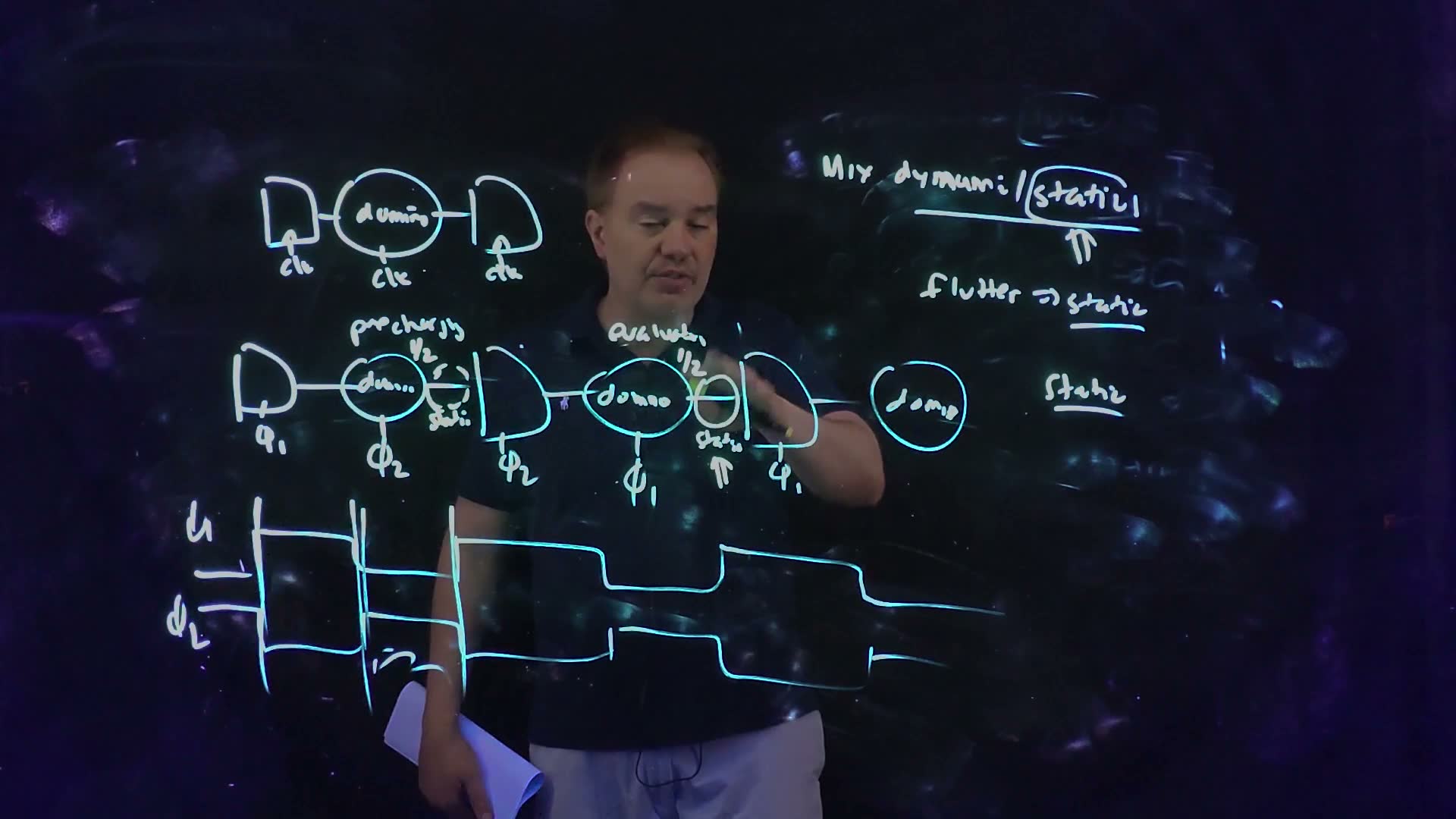
Fair copy of the board above (Lecture14 @ 37:49), mark for mark in its own layout. The board is written in one pen (cyan), so the copy is all black. The board of 33:07 stands unchanged. New are a static block after each domino of the second row, labelled “static” (the first drawn as a broken ring, copied dashed), with a double arrow under the second; and at the right “Mix dynamic/static” (“static” ringed, the ring open at its right end, the line underlined, a double arrow under it), “flutter ⇒ static” and “Static”. The φ1 latch behind the lecturer’s hand is read from 33:07 and 39:04. Scrawled words are set in full; the first “static” label, written across the bottom of its ring, is set just below it.
Flutter, computed for a domino block whose inputs never change and whose result is 1 (stage delays 0.05 cycle, a sketch). Its dynamic node N discharges in every evaluate and is restored in every precharge, so its output Z pulses every cycle, and a static gate after it, S, toggles every cycle too. The same static gate fed from a flip-flop whose output does not change, S′, never switches. Key: the domino’s clock, N its dynamic node, Z its output, S the static gate after it, S′ the same gate fed by a flip-flop.
Memorize it; Chapter 6’s is the case .
A worked example added. For example, a domino output node of at and , with its inputs constant and its result 1.
Who burns power on unchanged data (added)
- The domino output. It rises in every evaluate and falls in every precharge, so and . Its dynamic node also discharges and recharges every cycle.
- A static gate fed by the same unchanged flip-flop outputs. Nothing changes, so and .
- A static gate fed by the domino output. It flutters with it: another node, another for each node of the same size, for a result that never changes.
- The same domino with result 0. Its dynamic node never discharges, its output stays 0, and : domino burns power only for the results it evaluates to 1.
Traps.
- “Domino always burns more.” It is hazard-free; static logic’s glitches on changing data can cost more than domino’s regular activity.
- Forgetting the dynamic node. When the result is 1, the internal dynamic node cycles every time too, as well as the output.
- “Flutter is a logic error.” The static logic’s final value each cycle is correct; only the power is wasted.
Check yourself With its inputs constant, for which result does a domino block's output flutter, and why not for the other?
For a result of 1. The output goes to 0 in every precharge and back to 1 in every evaluate. For a result of 0 the dynamic node never discharges, so the output stays 0 through both phases and nothing toggles.
Check yourself A static gate with C = 10 fF sits after a domino output that evaluates to 1 every cycle, at VDD = 1 V and f = 2 GHz. What is its flutter power?
It toggles once each way per cycle, so : , all of it wasted: the gate’s value at the end of each cycle is the same every time.
10. Cycle-boundary and mid-cycle latches
You need
The two-phase domino chain (Section 8). latch, domino on , latch, domino on , latch, and so on, with and complementary. Each domino block precharges while its clock is low, and its output is then 0. The latch after each block closes when the block’s clock falls and holds its result while the block precharges.
Domino is monotonic (Chapter 11 §4–6). In evaluate a dynamic node can only fall. Once it has discharged it stays down until the next precharge, even if the input that discharged it falls again.
Delayed reset (Chapter 12 §7). A footless domino stage avoids a collision if its precharge starts only after the stage feeding it has precharged. Its clock keeps the same rising edge and falls later, by about the previous stage’s precharge time. The idea there, and here, is to move one clock edge relative to another so that a stage acts on its input before that input goes away.
The question. Every domino block in Section 8 is followed by a latch. Are all of those latches needed?
Two kinds of latch
Cycle boundaries and the latches between them (board, 37:50–39:28)
- Cycle-boundary latches. Usually the latches mark the cycle boundaries of the RTL, the register-transfer description of the design: the state the logic designer sees each cycle is in them (37:50–38:43) board. The board draws a vertical line through each latch.
- Mid-cycle latches. The latches then sit in the middle of each cycle: “mid-cycle latches” board. They exist only because the cycle’s logic is split into two domino blocks.
- What a mid-cycle latch does. When falls, the block starts to precharge and its output drops to 0 ("" on the board). The mid-cycle latch closes at the same edge and keeps the evaluated value for the block that follows (38:43–39:28) board.
Cycle-boundary and mid-cycle latches. The latches (vertical lines) mark the RTL’s cycle boundaries; the latch between them is a mid-cycle latch (arrow). When falls, the block precharges and its output goes to 0 (), which is why the latch is there. With a small overlap of the phases it can be removed (dashed, ✗). Lecture14 @ 39:49.
The board (Lecture14 @ 39:49)
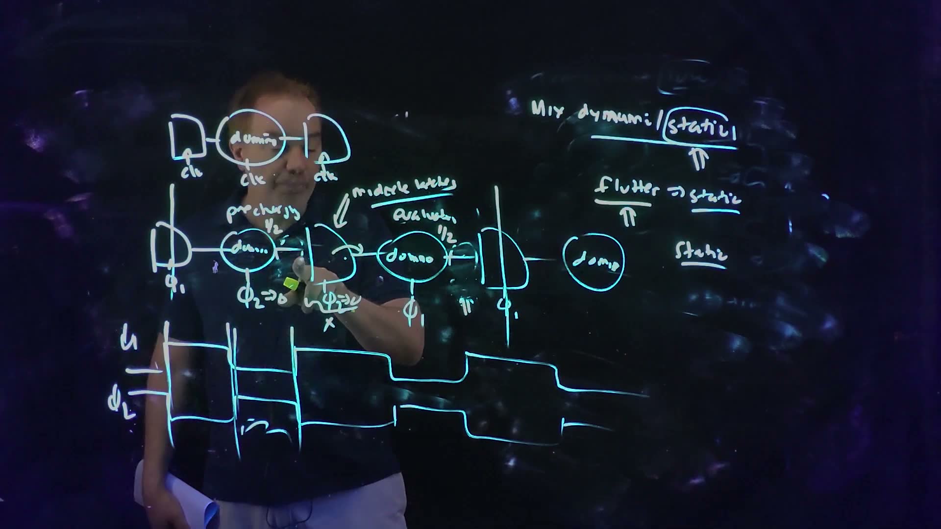
Fair copy of the board above (Lecture14 @ 39:49), mark for mark in its own layout. The board is written in one pen (cyan), so the copy is all black. Since 37:49 the static blocks have been wiped: pieces of the first ring and the upper part of the second still stand and are copied as they stand, with the double arrow under the second; both “static” labels are gone. New are the vertical lines through the φ1 latches, “midcycle latches” with its arrow to the φ2 latch, the curved arrow from that latch, “⇒ 0” after each φ2, the squiggle, underline and cross under the φ2 latch, and the underline and double arrow at “flutter”. The top row’s domino, behind the lecturer’s head, and the marks round his hand under the φ2 latch are read from 40:32, where the board is unchanged. The scrawled “midcycle latches” is set in full. The φ1 labels, crossed by the new lines on the board, are set just right of them, and the marks under the φ2 latch are spaced a little to clear the typeset φ2.
Dropping the mid-cycle latch
Overlap the phases a little (board 39:28–40:07; the timing is added)
- Remove the latch and wire the block straight into the block. The danger: the block’s output falls to 0 when falls, which with complementary clocks is exactly when rises and the block starts to evaluate. The block would see its input vanish as it starts.
- Make rise slightly before falls (39:28–40:04) board: “a slight overlap window between phi one and phi two”. For a short time both phases are high. The block is still evaluating, so its output is still valid, and the block has already started to evaluate on it.
- Why the value survives added. In those the first domino stage of the block evaluates: if its input is 1, its dynamic node discharges. When then falls and that input drops to 0, the discharged node stays down, because domino is monotonic. The block has “absorbed” the value, and nothing needs to hold it. This is the same move as Chapter 12’s delayed reset: one stage acts on its input before the edge that takes the input away.
- “The kinds of tricks” used “in very aggressive custom microprocessor designs” (40:07) board.
Dropping the mid-cycle latch (added; a sketch with the overlap exaggerated). rises before falls. In that window the block’s output is still valid, and the first dynamic node of the block evaluates on it and discharges. When falls and that output drops to 0, the discharged node stays down, because domino is monotonic, so no latch is needed to hold the value. The overlap must cover the stage’s evaluate time: . is the block’s output; the first dynamic node of the block.
What breaks it added. While both phases are high, the cycle-boundary latch in front of the block is already open while that block is still evaluating. New data coming through that latch must not reach the block within , or it corrupts the value being handed on. That is a hold condition, Chapter 14’s race-through in another form: the overlap that removes a latch has to be paid for with a short-path check.
Derive it in three lines: (1) the block’s output is valid only until falls; (2) the block’s first stage can start only when rises, earlier; (3) it must finish discharging before its input goes, so .
A worked example added. For example, the first stage of the block takes to evaluate.
The cost of the overlap (added)
- The overlap. ; at that is 4% of the cycle.
- What it costs the block. Its result must be ready when rises, 40 ps before falls. Its half-cycle budget falls from 500 ps to .
- What it saves. A latch, its clock load and its delay in the middle of every cycle.
Traps.
- The name clash. Chapter 14’s board calls the non-overlap window, in which both phases are low, . here is the opposite: a deliberate overlap, both phases high. This page uses a different symbol so the two are not confused.
- Overlapping at the wrong edge. What matters is rising before falls. Moving the other pair of edges (at falling) does nothing for this latch.
- Dropping a cycle-boundary latch. The RTL’s state lives in the latches; only the mid-cycle ones can go.
Check yourself Why does the φ2 block's output fall when φ2 falls?
When falls the block precharges: its dynamic nodes are pulled back to 1, so the inverters after them, its domino outputs, go to 0. A domino output is 0 throughout precharge, whatever the block evaluated.
Check yourself The φ1 block's first stage evaluates in 30 ps, and the design wants 10 ps of margin on top. What overlap is needed, and how much of its half-cycle can the φ2 block use at Tcycle = 800 ps?
. The block’s half-cycle is 400 ps, and its result must be ready before falls, so it has .
11. Background for the final: number representation and overflow
You need
Binary addition added. Add column by column from the least significant bit; a column whose bits and incoming carry add to 2 or 3 writes 0 or 1 and carries 1 into the next column. An -bit word has bits numbered 0 to .
Background for the final: the lecture spends its last 18 minutes here, as the start of the adders in Chapter 16. No worked example; the two checks are enough.
Where the course goes next board. A microprocessor’s circuits come in three kinds (40:48–44:37): the datapath (dataflow), structured and often custom; control logic, “random” (unstructured) and therefore automated or semi-automated, since that is where “99.99 %” of the bug fixes before tape-out land (43:48); and arrays (memory), structured. The next chapters follow that order. Numbers come in fixed point (integers) or floating point (a mantissa and an exponent, for a large dynamic range) (45:39–46:32). The lecturer once saw a workstation whose floating-point register file, damaged by electromigration (Chapter 23), gave 1 + 1 = 2.05 while the operating system, all fixed point, ran normally (47:26).
The board (Lecture14 @ 48:13)

Fair copy of the board above (Lecture14 @ 48:13), mark for mark in its own layout. The board is written in one pen (pink, orange where the ink is still fresh), so the copy is all black. The ring round “floating point” is new at 48:13 and is drawn over the word’s earlier underline, whose right end runs into the ring. The board’s scrawled words are set in full, and its arrows written “=)” are set as ⇒.
Two’s complement board. Three bits read as unsigned give 000 … 111 = 0 … 7. Read as two’s complement, they sit on a circle: 000 = 0, 001 = 1, 010 = 2, 011 = 3, then 100 = −4, 101 = −3, 110 = −2, 111 = −1 (49:27–51:27). The first bit is the sign bit. To negate, take the ones’ complement and add 1: 001 → 110 + 1 = 111 (−1), and 010 → 101 + 1 = 110 (−2) (51:41–52:12).
Three-bit two’s complement: the eight codes on a circle, each with its signed value. Counting up runs clockwise; the first bit (the sign bit, MSB) is 1 for the negative values. Between 011 (3) and 100 (−4) the signed values wrap (mark), which is where an addition overflows. Lecture14 @ 51:51.
The board (Lecture14 @ 51:51)

Fair copy of the board above (Lecture14 @ 51:51), mark for mark in its own layout. The board is written in one pen (pink, orange where the ink is fresh), so the copy is all black. The board of 48:13 has been partly wiped: “Microprocessor”, the right end of the top ring with “low ⇒ structured” (the end of “dataflow”), one stroke of the ring’s left end, and “automated” and “semi-automated” still stand and are copied as they stand. “001 →” is being written at 51:51; it is finished as “001 → 110 + 1 ⇒ 111” by 54:35. Scrawled words are set in full; the “−4” beside 100 is set on the line so that it does not read as an exponent.
The board (Lecture14 @ 54:35)
Fair copy of the board above (Lecture14 @ 54:35), mark for mark in its own layout. The board is written in one pen (pink, orange where the ink is fresh, as the carry rings), so the copy is all black. The codes stand as at 51:51, and the strokes left from 48:13 still stand. Since 51:51 “automated”, “semi-automated” and the signed and unsigned notes at the right have been wiped; “Overflow” is written where “automated” stood. The lecturer’s head is in front of the ring’s right end; the ink reads through. Scrawled words are set in full; “Overflow” and the two negation rows are levelled, and the negation rows are set a size smaller so that their terms keep clear of each other.
Overflow board. Adding 2 + 2 gives a code that reads −4: the sum has run past 3 and wrapped round the circle. The test compares two carries, the one into the MSB column and the one out of it (52:48–54:09):
In the first sum, 2 + 2, the carry into the MSB is 1, the carry out is 0, and the answer 100 is wrong (overflow). In the second, 2 + (−2), both carries are 1 and the answer 000 is right. The adder reports overflow as a condition code (54:13), written below as the flag (1 for overflow; not a voltage).
Endianness board. A<0:31> numbers bit 0 as the MSB (big-endian, IBM); A<31:0> numbers bit 0 as the LSB (little-endian, Intel). Either works; mixing them does not (55:42–58:13). The lecture adds, in speech only, that the same holds for the order of bytes.
The board (Lecture14 @ 58:13)

Fair copy of the board above (Lecture14 @ 58:13), mark for mark in its own layout. The board is written in one pen (cyan), so the copy is all black. A⟨0⟩, at the bottom, is new since 57:28. The lecturer stands in front of “point number”, the arrows and “big”; the ink reads through. The board’s lower-case-looking “a” is set as the page’s A, its angle brackets as ⟨ ⟩, and the scrawled words in full.
Memorize all three. Traps: the carry out alone is not overflow (2 + (−2) carries out 1 and is right); an unsigned wrap is not a signed overflow (in 2 bits, 11 + 01 = 00 carries out for unsigned, and is −1 + 1 = 0 for signed, with no overflow); and −4 has no positive partner in 3 bits (100 → 011 + 1 = 100).
Check yourself In 3 bits, is 011 + 001 an overflow?
Bit 0: 1 + 1 = 0, carry 1. Bit 1: 1 + 0 + 1 = 0, carry 1 into the MSB. Bit 2: 0 + 0 + 1 = 1, carry out 0. The carries into and out of the MSB differ (1 and 0), so it overflows: 3 + 1 gives 100, which reads −4.
Check yourself PS5-Q2 asks for a two-bit wrap-around counter, 00 → 01 → 10 → 11 → 00, with a synchronous reset to 00. Write the next state of each bit.
Counting adds 1 modulo 4. Bit 0 always flips: . Bit 1 flips when the carry out of bit 0 is 1, that is when : . From 11 both flip to 00, which is the wrap-around. With the reset, AND each with : and . (fs2 solves the whole problem, with its timing.)
On the exam
No past final tests this chapter’s circuits directly: dynamic flip-flops, C²MOS, TSPC, two-phase domino and number representation do not appear on FN10, FN12, FN17 or FN19, or on any midterm. They are still in the final’s scope (the final is cumulative). Two items point at what may come: the lecturer’s own flag, “That might be a very good exam question” (27:02), and this term’s problem set. FN17-5’s latch timing, which a first plan placed here, is Chapters 13–14’s (5d at Chapter 14’s non-overlap window).
| Item | Points | What it asks | Sections | Solved on |
|---|---|---|---|---|
| PS5-Q2, logic and reset | none stated (a design problem) | a two-bit wrap-around counter with a synchronous reset arriving 20 ps after the rising edge, for the fastest clock | §11 (next-state logic: Check 2); §6 (a single-clock edge-triggered flip-flop and its inverted output: the counter trap); the reset’s setup and hold are Chapters 13–14 | fs2 (to come) |
| The lecturer’s flagged question (27:02) | — | half latches on the TSPC flip-flop, or its negative-edge version | §6 (Checks 1 and 2), with §4–5 for the method | §6 here; a variation on fs2 |
The question forms to expect, from the lecture’s own phrasing:
- “Is this flip-flop positive- or negative-edge triggered?” Read the master’s gate polarities (§1, §6).
- “Why does this circuit have a race / why does it not?” Find the overlap windows of clk and and which devices they turn on (§2); for C²MOS, the one-way-pull argument (§3).
- “Which nodes are dynamic in which state?” Walk the stages through each clock phase and data sequence (§4–6).
- “Add one transistor to improve the noise robustness.” Find the state with two floating nodes and hold the inner node with a half latch gated by the output (§5–6).
- “Compare these clocking styles for this logic.” for flip-flops, two-phase domino and static latches (§7–8).
- “Which is lower power, static or domino?” It depends, with both reasons, and flutter (§9).
Memorize.
- A race: the function depends on which of two delays is faster (12:05).
- The active edge is the master’s closing edge: a master transparent while clk = 0 makes a positive-edge flip-flop.
- Clocked NFETs make a TSPC latch transparent-high; clocked PFETs make it transparent-low.
- The half latch: the device that drives Y to the value it must keep (PFET for 1, NFET for 0), gated by the output.
- The TSPC flip-flop: at the rising edge.
- .
- Two’s complement: range ; ; overflow .
Derive (each in about three lines).
- The slowest clock (§1). gives ; set for ; each node floats for , so .
- The race (§2). After clk falls, both gates conduct for ; D reaches the slave’s node after ; so . After clk rises, the same overlap is a hold time of about .
- No race in C²MOS (§3). In the both-0 window only clocked PFETs are on, so both stages can only pull up; X rising turns the slave’s pull-up off and X cannot fall; the both-1 window is the mirror.
- Clocking domino (§7–8). Flip-flops: the domino gets one evaluate half, . Two-phase domino: , so , against for static latches.
- The overlap (§10). The output lasts until falls; the block starts earlier; its first stage must have evaluated by then, so .
Method cards. The playbook’s “storage-cell design” and “clock generation” cards, written with fs2, will cover these families.