FM1. Final practice: SRAM, decoders and memory addressing
This page practises the final’s memory questions: how long an SRAM takes to answer, from the address to the data, and where that time goes; how a memory’s address is split between the rows and the columns; how a decoder picks one row and what a decoder-driven ROM outputs; and how the course’s dynamic row decoder is clocked so that it never raises the wrong word line. Every past-final part on these topics is here, re-solved from the papers; the keys’ answers are not copied, and where a key slips the page says so. The parts come in three families: the SRAM access path (FN10-5a–c), addressing and decoders (FN10-10a–b, FN12-10d) and the dynamic row decoder and its clocks (FN17-6a–b). Each family opens with a How to approach section that gives the model and the moves once, and ends with harder added variations: longer chains, setups no past paper uses, and heavier arithmetic, as the real Fall 2026 midterm was.
Every part is worked the same way: what it asks, the idea, why this formula, the solution in steps (each gives its reason first), a check by another route, the answer, and what to remember. Try each part first; open the Hint if you are stuck. The answer key’s verdict is folded at the end of each past-paper part.
Before you start. Everything here is taught in Chapter 19 and Chapter 18 §10, on the delay model of Chapter 8 and Chapter 12, and each section below restates what it uses:
- a stage’s delay as its gain, and a dynamic stage’s evaluation edge (Chapter 8 §1, Chapter 12 §2);
- the 6T cell, the read column and the bitline’s delay (Chapter 19 §1, §7); the write column (§8); sense amplifiers (§10);
- decoders, predecoding and the ROM (§11); the race-based NOR, its clock condition and the decode path’s delay (§12); the access time (§13);
- the two phases and the non-overlap gap (Chapter 19 §6, Chapter 14 §3); the race between dynamic stages (Chapter 11 §5);
- the address split and the column multiplexer (Chapter 18 §10, Chapter 19 §9); pseudo-NMOS NOR columns (Chapter 10 §10).
Conventions on this page.
- Delays are in , the paper’s fan-out-of-one (FO1) delay: the guide’s . Capacitances are counted in µm of gate at fF/µm (FN10-5’s value), so a load of fF is µm. FO4 ≈ , as FN10-5c states.
- Clocks. and are the two non-overlapping phases: precharge while is high, access while is high; is the gap from falling to rising. The papers write phi1, phi2.
- Pages are the papers’ printed page labels.
Symbols
| Symbol | Meaning | Unit | First appears |
|---|---|---|---|
| the fan-out-of-one delay (the guide’s ) | ps | approach 1 | |
| gate capacitance per µm of width, 2 fF/µm here | fF/µm | approach 1 | |
| the equivalent width of devices in series, | µm | approach 1 | |
| an inverter’s PFET width | µm | approach 1 | |
| a stage’s gain: its load over its normalized inverter’s input; its delay in | — | approach 1 | |
| the word line’s capacitance | fF | approach 1 | |
| the bitline’s capacitance | fF | approach 1 | |
| , | the cell’s access and pull-down NFET widths | µm | approach 1 |
| the cells on one word line | — | approach 1 | |
| the bitline’s delay to | approach 1 | ||
| the bitline swing a detector waits for | V | approach 1 | |
| FO4 | the fan-out-of-four delay, | — | approach 1 |
| , , | the access clock, the precharge clock, and its complement | — | approach 1 |
| the non-overlap gap, falling to rising | ps | approach 3 | |
| , | the race-based NOR’s stage-1 and stage-2 nodes (this guide’s labels) | — | approach 3 |
| , | a memory’s number of words and its word width | —, bits | approach 2 |
| , | the physical array’s rows and columns | — | approach 2 |
| , | address bits into a decoder, and bits per predecode group | — | approach 2 |
| , | a decoder’s address input and its complement | — | FN12-10d |
| a ROM’s output column | — | FN12-10d | |
| FN17-6’s word lines | — | FN17-6 | |
| , | FN17-6’s bitline pair | — | FN17-6 |
How to approach an SRAM access-time question
Recognize it by the words: “decode path”, “wordline”, “race-based”, “domino NOR”, “precoded (predecoded) lines”, “bitline”, “access time”, “as a multiple of ”, “FO4”. The paper prints a chain of transistor-level stages with widths, gives the word line’s cells and wire, and asks for delays in ; a last part adds the bitline and compares the total with a processor’s cycle.
The model. A read is two jobs in a row. The decode path turns the address into one rising word line; then the selected cell pulls one bitline down far enough for a detector to see. Each is estimated with Chapter 8 §1’s rule: a stage’s delay, in , is its gain, the capacitance it drives divided by the input capacitance of the inverter that drives as hard. The bitline is just one more “stage”: the cell’s two NFETs in series driving a huge capacitor.
Why these, and their conditions. The gain rule: derive it from Chapter 8 §1. A pull-down of equivalent width drives like the inverter with NFET and PFET , whose input is ; the delay is the load over that input. A rising edge is pulled up by a PFET of , as strong as an NFET of , so the matching inverter’s input is . A dynamic stage evaluates through its input NFET and its foot in series (Chapter 12 §2); its precharge PFET is off then and does not count. The word line: derive it from the cell (Chapter 19 §1): each cell has two access NFETs, one to bit and one to , and both gates hang on the word line. Memorize the factor of 2. The bitline: derive it as one more stage (Chapter 19 §7); the “delay” of the gain model is the time to the 50 % point, which is exactly “from to ”.
The moves.
- Name each stage’s critical edge. A domino or race NOR’s edge is its fall (evaluation, through input and foot); an inverter after a dynamic node rises.
- Find each stage’s input: of the conducting NFETs, or for a rising inverter.
- Find each stage’s load: the next stage’s input gates (both devices of an inverter; only the NFET a dynamic stage’s node drives), times the fan-out; the word line from the formula above.
- Divide and add. Keep two decimals; add the unrounded gains if you can.
- The bitline: of access and pull-down, , divide. Scale for the swing the detector needs.
- The access time: decode plus bitline, then convert: FO4 ≈ .
Decide on the way: which edge of each stage is critical; which fan-out the paper means (the printed number, or the predecoder’s topology); which swing the detector needs ( unless told otherwise).
Traps. One access gate per cell on the word line (FN10-5’s key does this). Counting a dynamic stage’s precharge PFET as part of its load or drive. Forgetting the foot in series. Using instead of for a rising inverter. Taking only the access NFET for the bitline: the pull-down is in series with it.
FN10-5: the SRAM decode path, the bitline and the access time (26 points)
You need
A stage’s delay from its gain (Chapter 8 §1). In , a stage’s delay is the capacitance it drives over the input capacitance of the normalized inverter with its pull-down strength: NFET , PFET , input . Devices in series combine like resistors, . A rising inverter output is driven by its PFET, as strong as an NFET of half its width: input .
Domino and the race-based NOR (Chapter 19 §12, Chapter 12 §2). A dynamic NOR precharges its node high (PFET on), then evaluates (foot on): the node falls if any input is high, through that input and the foot in series. The race-based NOR’s stage 1 is precharged and footed on , so it evaluates as soon as falls; stage 2 is footed on , the clock qualification; an inverter drives the word line.
The cell and the bitline (Chapter 19 §1, §7). Each 6T cell has two access NFETs, both gated by the word line. A read discharges one bitline through the access NFET and the pull-down NFET in series.
The question (FN10-5, p7, in the paper’s words). As you learned in the design project, the access time of an SRAM is determined by the delay through the decode path as well as the time to perform the bitline access. Let’s consider these two components of the delay for a memory with 256 rows (8 bits of row address).
Consider the decode path shown above. Sixteen (16) domino NOR gates produce 16 precoded lines that then fanout two 256 race-based wordline decoders. Assume that the wordline drives 256 SRAM cells with access transistors and 100 fF of wire capacitance. Also assume that transistor gate cap is . All devices are minimum length. .
FN10-5’s decode path (Final 2010, p7, redrawn). Widths in µm, all devices minimum length; T bars are . The numerals I–V are this guide’s, and is the paper’s “wordline load”. The key’s handwriting on the scan (the stage names and “100fF + 256(2fF)”) is left out.
The exam’s own figure (FN10-5, p7)
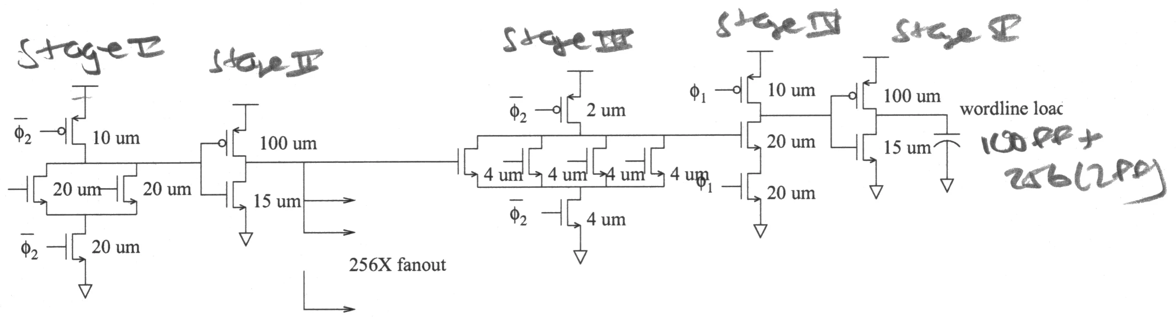
Reading the figure. Stage I is a domino NOR of two predecoder inputs (20 µm each; its 10 µm precharge PFET and 20 µm foot on ); stage II its output inverter (100/15); the “256X fanout” arrows send each predecoded line to the race NORs. Stage III is the race NOR’s first stage, with four 4 µm inputs, one per predecoded group; stage IV is its clock-qualified second stage on ; stage V the word-line driver (100/15). “Precoded” and “fanout two” are printed so; read them as “predecoded” and “fan out to”.
Part (a): the decode path’s delay (10 points)
FN10-5a, p7. Estimate the delay of the decode path shown above (for the critical evaluation edge) as a multiple of the fanout-of-one (FO1) delay, . (10 points)
Hint
What it asks. One number, the delay from the address to the word line, in . The unknowns are five gains: each stage’s load and the drive of the devices that switch on its critical edge. The words that decide the method are “multiple of the fanout-of-one delay”: a gain-per-stage estimate, Chapter 8’s, added along the path. “Critical evaluation edge” says which transition of each stage to use: the evaluation, the edge the access waits for.
The idea. Each stage’s delay is its gain: what it drives over how hard it drives. The domino stages (I, III, IV) are judged on their falling evaluation edge, through an input NFET and the foot in series; the inverters (II, V) on their rising edge, through the PFET. The loads are the next stage’s input gates, with the fan-out where one output drives many; the last load is the word line, whose capacitance comes from the wire and the cells. The path’s delay is the sum, because the stages switch one after another: stages I–III finish before rises (they are the unselected rows’ race), and IV–V run after it (the selected row), so with placed just after stage III the address-to-word-line time is all five.
Why this formula. for a falling stage, for a rising one, and .
- Where it comes from. A stage that pulls down through drives as hard as the inverter with NFET and PFET , input ; its delay in is its load over that input (Chapter 8 §1). A PFET of drives like an NFET of , so a rising inverter’s matching input is (Chapter 12 §2).
- Series devices. On evaluation, a NOR’s node falls through one input (the worst case: a single input high) and the foot: . Parallel inputs do not help the worst case.
- The word line. Each 6T cell has an access NFET to bit and one to , both gated by the word line (Chapter 19 §12): 2 gates per cell.
- Conditions. The stages’ own drain capacitance is ignored, and the load is gate capacitance at 2 fF/µm, plus the stated wire. The precharge PFETs are off on the evaluation edge and add nothing. A stage’s load counts only the gates its output drives: stage III’s node drives only stage IV’s 20 µm NFET; an inverter’s input is both its devices.
- The tempting alternative. Counting one access device per cell: fF. It forgets the second access NFET, the one to .
FN10-5a
- Stage I, the domino NOR falls. Because its node falls through one 20 µm input in series with the 20 µm foot, µm and its normalized input is µm. Its load is stage II’s inverter, µm. Gain .
- Stage II, the predecoded line rises. Because the inverter’s output rises through its 100 µm PFET, its normalized input is µm. Its load is the paper’s “256X fanout” of race-NOR inputs, 4 µm each: µm. Gain .
- Stage III, the race NOR falls. Because an unselected row’s node falls through one 4 µm input and the 4 µm foot, µm, input µm. Its node drives only stage IV’s 20 µm NFET. Gain .
- Stage IV, the clock-qualified stage falls. Because on the selected row stage III’s node stays high and opens the foot, the node falls through 20 µm and the 20 µm foot: , input 30. Load: stage V’s inverter, 115 µm. Gain .
- The word line’s load. Because each of the 256 cells puts two 1 µm access gates on it: fF, which at 2 fF/µm is 562 µm of gate.
- Stage V, the word line rises. Because the driver’s 100 µm PFET pulls it up, its normalized input is 150 µm. Gain .
- Add. . Of this, (stages I–III) must fit before rises, and (IV–V) comes after it.
FN10-5a’s five gains (new figure, computed in the page’s test): each stage’s load over its normalized input. The arrow in each box is the stage’s critical edge (I, III and IV fall on evaluation; II and V rise). Stages I–III, , must finish before rises (dashed); IV–V, , follow it: in all.
Check. By the path’s effort (Chapter 8 §2): the product of the five gains is about 1253, and five equal gains with that product would be each, in all. The sum of gains with a fixed product is smallest when they are equal, so 21.57 must lie above 20.8, and it does, by only 3.6 %: the path is well balanced, and the answer has the right size. The largest gain, stage II’s 6.83, is the one that a resize would attack. By the units: every gain is µm over µm, and the word line’s 562 µm is 512 access gates of 1 µm plus the wire’s 50 µm.
Answer: about (), with the word line at fF.
Remember. Name each stage’s critical edge before you divide: falling dynamic stages through input and foot (), rising inverters through the PFET (). Two access gates per cell on the word line. A decode-path question is five small divisions; the marks are in the loads.
A remark on the fan-out (the paper’s “256X fanout” is used above). Eight row bits in 2-bit groups make predecoded lines, and each 4-input race NOR takes one line from each group, so one line is shared only by the rows whose two bits in its group match it: race NORs (Chapter 19 §11). With that fan-out, stage II’s load is µm, its gain , and the path . The answer keeps the printed 256, as the paper asks; say which you used.
The answer key differs
Part (b): the bitline’s delay (10 points)
FN10-5b, p8. Estimate the delay of the read access of an SRAM cell (as a multiple of ) assuming that the bitline must be pulled from to for detection. To do this, assume that the nFETs of the 6-T SRAM cell have width and that the total capacitance of the bitline is 250 fF. (10 points)
Hint
What it asks. The time for the selected cell to pull a precharged bitline halfway down, in . The unknowns are the drive (the cell’s devices in the discharge path) and the load (250 fF). The phrase “from to ” decides the method: that is the gain model’s 50 % delay, so the bitline is one more gain.
The idea. After the word line rises, the cell node that holds 0 is connected to its bitline through the access NFET, and held at ground by the pull-down NFET. The bitline’s charge flows through both, in series, to ground. So the cell is a weak gate (two 1 µm devices in series) driving an enormous load (the whole column’s wire and drains), and its delay is the ratio, exactly as for any stage.
Why this formula. with .
- Where it comes from. The access and pull-down NFETs in series drive like one NFET of ; the inverter with that pull-down has input ; the load in µm is (Chapter 19 §7).
- Conditions. The gain model’s delay is to the 50 % point, which is the question’s . “The nFETs … have 1 µm width” sets both and . The 250 fF is the total, so nothing is added for drains.
- The tempting alternative. Using the access NFET alone (, input 3, gain 41.7). The pull-down is in series with it; leaving it out halves the delay.
FN10-5b
- The drive. Because the access and pull-down NFETs are in series, µm, and the matching inverter’s input is µm.
- The load. Because gate capacitance is 2 fF/µm, the 250 fF bitline is µm of gate.
- The delay. Because the bitline must reach , the 50 % point: .
Check. By scaling Chapter 19’s example column (§7), 120 fF with µm, which takes : the delay goes with , so . By size: the bitline is about four times the decode path (21.57), at the top of the two to four times that Chapter 19 §13’s example finds; there, as here, the bitline dominates.
Answer: about ().
Remember. The bitline is one gain: two cell NFETs in series against the column’s capacitance. It is by far the largest term in a read.
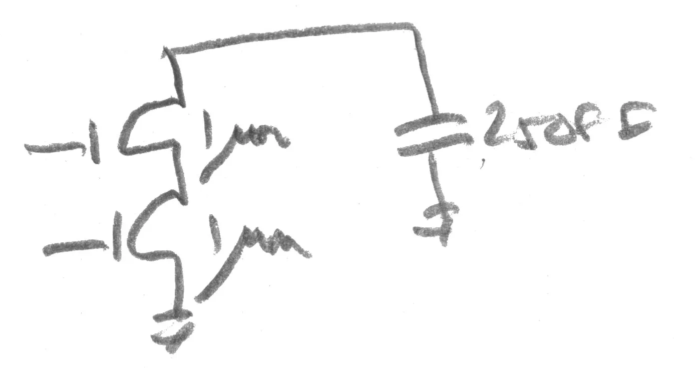
The key’s sketch (FN10-5b, p8, the key’s handwriting)
The answer key agrees
Part (c): the access time, the cycle and a remedy (6 points)
FN10-5c, p8. If the fanout-of-four delay (FO4), , what is the approximate memory access time as a multiple of ? If a typical processor has a cycle time of 12-15 FO4, with most cycles including a memory access, why might this be a challenge? Name one technique for improving SRAM access time. (6 points)
Hint
What it asks. Three things: the access time in FO4; why that number troubles a processor; and one way to make it smaller. The words “most cycles including a memory access” decide the second answer: the comparison is with one cycle.
The idea. A read is the decode path followed by the bitline; the two add. The paper’s conversion, , turns the total into FO4. A cycle is 12–15 FO4, so an access that needs more than that cannot be done in one cycle; a processor that needs one almost every cycle must either stretch its cycle or spread each access over several. The remedies attack the larger term, the bitline.
Why this formula. and FO4 ≈ .
- Where it comes from. The bitline cannot start to fall until the word line is up, so the delays are in series (Chapter 19 §13).
- Conditions. The detector waits for (5b’s assumption); the detector’s own delay and the data’s path out are left out, as the question does. The conversion is the paper’s.
- The tempting alternative. Converting with FO4 = (“fan-out of four”). That holds only when the driver’s own drain capacitance is ignored (Chapter 7’s model). Counting it, an inverter driving four copies of itself charges against FO1’s , so with (Chapter 5 §13): 4 with no drain capacitance, 3 at . The paper fixes 3; use it.
FN10-5c
- The access time. Because the bitline starts only when the word line is up: .
- In FO4. Because : FO4.
- Against the cycle. Because a cycle is 12–15 FO4, the access takes to cycles. With a memory access in most cycles, the processor must either run a cycle about three times longer, or pipeline each access over three cycles (and stall when the next instruction needs the data at once).
- Where the time goes. Because the bitline is of the total, a remedy should shorten the bitline’s term.
- A technique. Because the bitline falls roughly linearly near , a sense amplifier that fires on a swing of 50–100 mV instead of 1.25 V cuts that term by more than ten times (Chapter 19 §10). Others: shorter bitlines (fewer rows per bank, Chapter 18 §10), a skewed detector that switches near (§7), self-timing, pipelining the access.
FN10-5c’s access time (new figure, computed): decode (hatched) plus the bitline’s 83.33, in all. The thin dashed bar is the key’s , with one access gate per cell. Dotted: a 12 and a 15 FO4 cycle (36 and at FO4 = ; top axis in FO4). The access spans about three cycles, and the bitline is 79 % of it.
Check. By the parts: the sum is no smaller than its larger term, FO4, which alone is already about two cycles of 12–15 FO4; so the conclusion, “more than one cycle”, does not depend on the decoder’s exact number. With the fan-out remark’s 16.45, the total would be 99.8 , still 33 FO4.
Answer: about 35 FO4 (, divided by 3). That is 2.3–2.9 cycles of 12–15 FO4: an access cannot finish in one cycle, so a processor that reads memory in most cycles must slow its clock about threefold or pipeline the access over about three cycles. One remedy: sense the bitline with a sense amplifier at a small swing (50–100 mV), which cuts the dominant bitline term by more than ten times; others are shorter bitlines (banking), a skewed detector, self-timing and pipelining.
Remember. Access time = decode + bitline; the bitline dominates, so the remedies are all about the bitline: a smaller swing (sense amplifiers) or a smaller capacitance (banks).
The answer key differs
Harder variations: the SRAM access path
You need
The gains (Chapter 8 §1, Chapter 12 §2). A falling stage’s gain is , with the conducting NFETs in series (an input and the foot); a rising inverter’s is . FN10-5’s stages: I , II , III , IV , V .
The word line and the bitline (Chapter 19 §7, §12). ; to , and for a swing , .
Predecoding (Chapter 19 §11). bits in groups of : lines, inputs per decoder, each line feeding decoders.
These variations added are harder than FN10-5 in the ways the real midterm was: Variation 1 is a six-step chain that rebuilds the whole estimate for a larger array and then fixes it; Variation 2 changes the detector, an unfamiliar setup that moves the bottleneck from the bitline to the decoder; Variation 6, in the third family, turns the decode path into a clock budget in picoseconds. The budgets assume the practice finals’ pace, about 1.8 minutes a point. No key exists, so there is no key verdict.
Variation 1: a 512 × 512 array from the same circuits (about 25 minutes)
Variation 1: a 512 × 512 array from the same circuits
added The question. FN10-5’s memory grows to 512 rows and 512 columns, built from the same circuits with the same widths. The 9 row bits are predecoded in three 3-bit groups (each predecoder a domino NOR3 with FN10-5’s 20 µm inputs and foot), and each row’s race NOR has three 4 µm inputs. The word line’s wire doubles to 200 fF, and the bitline to 500 fF (both in proportion to length, for example). (a) How many predecoded lines are there, and how many race NORs does each drive? (b) Find the word line’s load and stage V’s gain. (c) The decode path’s delay. (d) The bitline’s delay to , the access time in and in FO4. (e) Split the array into two banks of 256 rows (the ninth row bit picks the bank): the new access time in FO4? (f) Resize stage V’s PFET (keeping the 100 : 15 ratio) so stages IV and V have equal gains: what width, and what do IV and V then cost?
Hint
What it asks. The whole FN10-5 estimate again for a bigger array, then two ways to win back time: one structural (banks), one by sizing. The unfamiliar part is deciding which stage sees which dimension.
The idea. Rows and columns act on different stages. More rows means more race NORs and longer bitlines: the predecoder’s fan-out (stage II) and the bitline grow. More columns means a longer, heavier word line: stage V grows. Stages I, III and IV see neither, so they keep their gains. Banking cuts the bitline back; sizing balances the last two stages.
Why this formula. The gains above; the predecode counts and ; and, for (f), equal gains minimize a sum with a fixed product.
- Where it comes from. Stage IV’s load is stage V’s input, ; stage V’s input is . The product of their gains, , does not depend on , so their sum is smallest when the two are equal (Chapter 8 §2).
- Conditions. A NOR3 predecoder evaluates through one input and the foot, as the NOR2 did, so stage I’s gain is unchanged; the wider gates’ extra drain capacitance is ignored, as in FN10-5.
Variation 1
- (a) The predecoder. Because 9 bits in 3-bit groups make 3 groups of one-hot lines, there are 24 lines; each race NOR takes one line per group (3 inputs), and each line is shared by the rows that match it in its group: race NORs.
- (b) The word line. Because each of 512 cells puts two 1 µm gates on it, fF µm, and stage V’s gain is .
- (c) The decode path. Because stages I, III and IV see neither dimension, they keep 3.83, 3.33 and 3.83; stage II now drives µm, gain 1.71. Total: . This is below FN10-5a’s 21.57 only because that answer uses the printed 256X fan-out. On the same fan-out of 64 (FN10-5’s 16.45), the bigger array decodes slower, all of it in stage V’s heavier word line.
- (d) The bitline and the access. Because the bitline doubles to 500 fF µm against the same µm: . Access: FO4, four to five cycles.
- (e) Two banks. Because each bank’s bitline spans only 256 rows, it is back to 250 fF and ; the decode is unchanged (the ninth bit enables one bank). Access: FO4.
- (f) Balance IV and V. Because the sum is smallest at equal gains: , so µm (NFET 21 µm). Each gain is then 5.36, and IV + V cost 10.72 instead of .
Variation 1’s three arrays (new figure, computed): decode (hatched) plus bitline, in . The 512 × 512 array doubles the bitline to (186.9 in all); two banks of 256 rows keep 83.3 (103.5). Dotted: a 12 and a 15 FO4 cycle (36 and ).
Check. By ratios: doubling the rows doubled the bitline term exactly (), and doubling the columns roughly doubled stage V’s load () and gain; the stages that see neither dimension did not move. In (f), the product equals , as it must.
Answer: (a) 24 lines, each driving 64 race NORs. (b) 2248 fF, gain 7.49. (c) . (d) ; access FO4. (e) FO4. (f) µm; IV + V 10.72 instead of , a small gain beside the bank’s .
Remember. Rows load the predecoder and the bitline; columns load the word line. The bitline is the term worth fighting, and banking is the structural fix; sizing the driver only polishes the decoder.
Variation 2: the detector decides the bottleneck (about 20 minutes)
Variation 2: the detector decides the bottleneck
added The question. FN10-5’s array keeps its decode path () and its column ( to at V). (a) The detector is a skewed inverter that switches at : how long does the bitline take now? (b) A sense amplifier fires at a 100 mV swing instead (its regeneration left out): how long? (c) Give both access times in and FO4, and say which fits a 12–15 FO4 cycle. (d) In each design, what share of the access is the bitline? (e) With the sense amplifier, which term is now worth attacking, and what does the fan-out remark’s 64 (path 16.45) give? (f) For example, widen both cell NFETs to 2 µm: the bitline to , and with the sense amplifier?
Hint
What it asks. The same array with two other detectors, and the consequence: the share of each term changes, and with it the right place to optimize.
The idea. Near the cell’s current is roughly constant, so the bitline falls about linearly: the time is proportional to the swing the detector waits for (Chapter 19 §7, §10). A detector that needs less swing shortens only the bitline’s term; once that is small, the decoder is the larger term.
Why this formula. .
- Where it comes from. A constant current discharges at a rate , so the time for is , proportional to ; the 83.3 is for V.
- Conditions. The current is near-constant for small swings (the cell’s NFETs stay saturated); for approaching this is the course’s approximation, not an exact result.
Variation 2
- (a) The skewed inverter. Because it switches at V, the bitline must fall 0.5 V: .
- (b) The sense amplifier. Because it fires at 0.1 V: .
- (c) The access times. Because decode and bitline add: skewed, FO4, more than one 15 FO4 cycle; sensed, FO4, inside even a 12 FO4 cycle.
- (d) The shares. Because the shares are each term over the total: the bitline is of the skewed design’s access, but only of the sensed one’s.
- (e) The next target. Because the decoder is now 76 % of the sensed access, it is the term to attack. With the topology’s fan-out of 64 the path is , and the sensed access FO4.
- (f) A stronger cell. Because doubles to 1 µm, the input is 3 µm and ; sensed, . The cell grows, and with it every bitline’s drain load and the word line’s (this estimate ignores both): wider cells are the expensive remedy.
Variation 2’s detectors (new figure, computed): the same decode, (hatched), with the bitline’s time to a swing of , of 0.5 V (a skewed inverter switching at ) and of 100 mV (a sense amplifier). In brackets, the bitline’s share of the access. Dotted: a 12 and a 15 FO4 cycle (36 and ).
Check. By proportion: the three bitline times, 83.3, 33.3 and 6.67, stand in the ratio of their swings, . And (c)‘s sensed total, 9.4 FO4, sits under the 12 FO4 cycle with room for the sense amplifier’s own few of regeneration.
Answer: (a) . (b) . (c) Skewed: FO4, more than a cycle; sensed: FO4, fits. (d) 61 % and 24 %. (e) The decoder (76 %); with fan-out 64, FO4. (f) to , sensed, at the cost of a bigger cell and heavier lines.
Remember. The detector sets the swing, and the swing sets the bitline’s term. Once a sense amplifier has shrunk the bitline, the decoder is the bottleneck: always recompute the shares before choosing what to optimize.
How to approach an addressing or decoder question
Recognize it by the words: “logical organization”, “ bits”, “internal array”, “column multiplexing”, “how many bits of address”, or a picture of AND gates with bubbled inputs feeding a grid of transistors on vertical lines, with “complete the logic table”. Nothing is timed; the marks are for the counting and for reading the circuit exactly.
The model. A memory of words of bits is what the user sees: give an address, get one word. Inside, the same cells are folded into a near-square array of rows by columns, so each row holds words. A row decoder raises one of the word lines; a column multiplexer picks one word out of the on that row (Chapter 18 §10, Chapter 19 §9). A decoder is one AND per output, each taking every address bit, true or complemented, so that exactly one AND is high for each address (Chapter 19 §11). Hung on pull-down devices over pseudo-NMOS columns, the same decoder is a ROM: a device where row crosses column pulls that column to 0 whenever row is selected (§11).
Why these, and their conditions. The split: derive it in one line. Each row holds words, so choosing a word takes one of rows ( bits) and one of words on it ( bits), and , so the bits add to . The ROM rule: derive it from pseudo-NMOS (Chapter 10 §10): the PFET pulls the column high unless a conducting NFET pulls it low, and only the selected row’s NFETs conduct. Each column is a NOR of the rows that have a device on it.
The moves.
- Address bits: (k means 1024). The word width does not enter.
- Row bits: .
- Column bits: words per row , then ; a :1 multiplexer.
- Check that the two add to step 1, and that .
- For a ROM: read each AND’s bubbles to find which input it decodes; list each row’s devices by column; the selected row’s devices make 0s, every other column is 1.
- Check a ROM by counting: the number of 0s in the table equals the number of devices.
Decide on the way: which input is the most significant (the order of the table’s columns, and the order the ANDs are drawn); whether a gate on a row line is a device’s gate or just a wire crossing (look for the gate bar).
Traps. Column bits as : the multiplexer chooses words, not bits. Reading a ROM device as a 1: it pulls its column low. Reading a device by the row its drain sits next to instead of the row its gate bar crosses.
FN10-10: address bits for a 4k × 16 memory (10 points)
You need
Binary addressing added. bits select one of things, so one of (a power of two) takes bits; “4k” is .
The array and the column multiplexer (Chapter 18 §10, Chapter 19 §9). The cells sit in rows by columns; a row decoder raises one word line, and a column multiplexer passes one word of bits out of the words on that row. Its selects are a full decode of the column bits.
The question (FN10-10, p17, in the paper’s words). Assume that I have a memory with a logical organization of .
FN10-10 prints no figure. This is the kind of array its question is about: Chapter 18’s SRAM array (Lecture17 @ 57:57, redrawn). Its numbers are Chapter 18’s example, not FN10-10’s: 1024 words of 32 bits stored as 256 rows of 128 columns, with a 10-bit address split 8 + 2 and 32 bits out. FN10-10’s memory is 4096 words of 16 bits in a 256 × 256 array. The row bits go to the row decoder at the left, the column bits to the multiplexer at the bottom.
Part (a): the address bits (4 points)
FN10-10a, p17. How many bits of address do I need? (4 points)
Hint
What it asks. The number of address bits for 4k words of 16 bits. The word “logical” decides the method: the count depends only on what the user sees, the number of words, not on how the cells are laid out.
The idea. An address names one word. With bits there are names, so the address needs the smallest with ; for a power of two, . The 16 bits per word come out together on one access and need no address bits.
Why this formula. Address bits .
- Where it comes from. Each bit doubles the number of names: names for bits (Chapter 18 §10).
- Conditions. “k” is 1024 in memory sizes, so 4k is a power of two.
- The tempting alternative. Counting bits: , “16 bits”. That would name every bit separately; the memory returns 16 at a time.
FN10-10a
- The number of words. Because k is 1024 here, 4k words.
- The bits. Because , 12 bits name every word exactly once.
Check. From a size you know: 1k = 1024 = words take 10 bits (Chapter 18’s 1024 × 32), and 4k is four times as many, two bits more: . Part (b)‘s split, , adds to the same 12.
Answer: 12 address bits ().
Remember. Address bits ; the word width never enters.
The answer key agrees
Part (b): the column-multiplexing bits (6 points)
FN10-10b, p17. If the internal array is organized to be , how many bits of the address are needed for column multiplexing? Explain. (6 points)
Hint
What it asks. How the 12 address bits divide between the row decoder and the column multiplexer when the 65,536 cells are laid out as a square, and why. “Explain” asks for the reason, not only the number.
The idea. The square array has 256 rows, so a row decoder needs 8 bits to raise one of them. A row then holds 256 cells, which is 16 words of 16 bits; the multiplexer under the columns must pick one of those 16 words, and that choice takes the remaining bits.
Why this formula. .
- Where it comes from. A word is found by its row and its place on the row; each row holds words (Chapter 18 §10).
- Conditions. : , so the array holds the memory exactly.
- The tempting alternative. column bits, choosing one of 256 columns. The multiplexer chooses 16-bit words, not single columns; 8 + 8 = 16 bits would address things, 16 times too many.
FN10-10b
- The row bits. Because 256 rows need one of 256 names, the row decoder takes bits.
- Words per row. Because a row holds 256 cells and a word is 16 bits, each row holds words.
- The column bits. Because the multiplexer must pick one of those 16 words, it is a 16:1 multiplexer driven by address bits, decoded into 16 one-hot selects (Chapter 19 §9).
FN10-10b’s split (new figure, to scale). The 256 × 256 array holds 4096 words of 16 bits, so each row holds 16 words. The row decoder takes 8 address bits; the selected row (thick) is 16 words, , of 16 cells each; a 16:1 multiplexer on the other 4 bits picks one word. The 12-bit address splits 8 + 4.
Check. By (a): bits, the logical count. By cells: .
Answer: 4 bits for column multiplexing. The 256 × 256 array uses 8 bits to pick one of 256 rows; each row holds sixteen-bit words, so a 16:1 column multiplexer, driven by the other bits, picks the word ().
Remember. Column bits , and row bits + column bits = address bits.
The answer key agrees
FN12-10d: a decoder-driven ROM table (9 points)
You need
A decoder (Chapter 19 §11). One AND per output; each takes every input, a bubble marking a complemented one, so each AND is high for exactly one input combination: the one with 0 at the bubbles and 1 elsewhere.
Pseudo-NMOS columns (Chapter 10 §10, Chapter 18 §2). A PFET with its gate grounded is always on and pulls its line up weakly; NFETs from the line to ground pull it down, and win, whenever their gate is high. The line is a NOR of the NFETs’ gates.
The question (FN12-10, p17, in the paper’s words). In this problem, we consider some of the combinational logic circuit styles we studied in the course. (d) For the following circuit, complete the logic table shown below. (9 points)
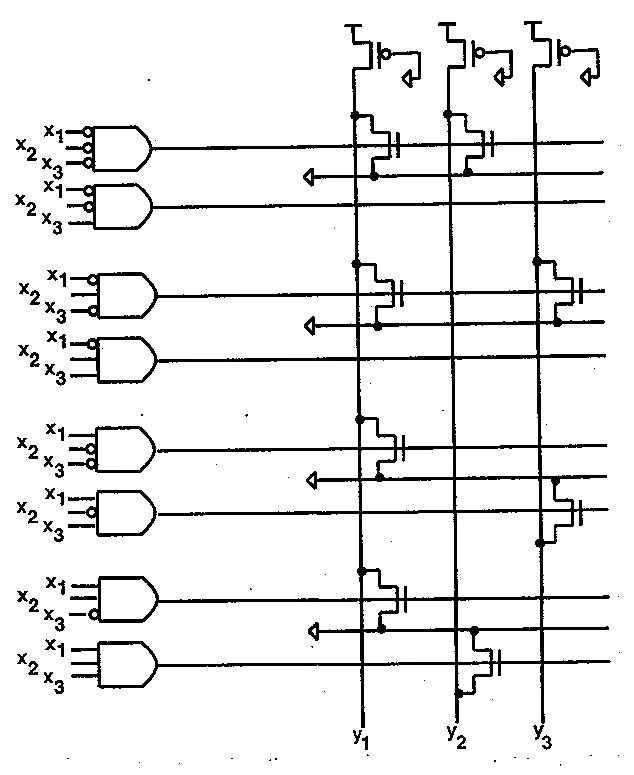
FN12-10d’s ROM (Final 2012, p17, redrawn). Eight 3-input ANDs decode (a bubble complements its input). The columns , , are pseudo-NMOS lines with grounded-gate PFET loads (T bars are ). The lines between row pairs are ground lines, and each NFET runs from a column to one of them. The paper draws each row through its NFET’s gate; here the gate is tapped from that row (a dot).
The exam’s own figure (FN12-10d, p17)
| 0 | 0 | 0 | |||
| 0 | 0 | 1 | |||
| 0 | 1 | 0 | |||
| 0 | 1 | 1 | |||
| 1 | 0 | 0 | |||
| 1 | 0 | 1 | |||
| 1 | 1 | 0 | |||
| 1 | 1 | 1 |
The table (9 points)
FN12-10d, p17. For the following circuit, complete the logic table shown below. (9 points)
Hint
What it asks. The three outputs for each of the eight inputs. The unknowns are which input each AND decodes and which columns each row’s devices pull down. “Logic table” says the answer is a truth table, read row by row.
The idea. The left half is a full 3-to-8 decoder: for each input exactly one AND is high. The right half is a ROM: three pseudo-NMOS columns, each held high by its always-on PFET, with NFETs that pull a column to ground when their row is high. So for each input, only the selected row’s devices act: they make their columns 0, and every other column stays 1. Each row of the table is one row of the circuit, read off its devices.
Why this formula. exactly when a device sits at (row , column ).
- Where it comes from. A column is a pseudo-NMOS NOR of the rows that have a device on it (Chapter 10 §10): low if any of those rows is high. Only one row is high at a time, so the column is low exactly when that row has a device on it (Chapter 19 §11).
- Conditions. Each NFET is stronger than its column’s PFET, so a single conducting device wins (the pseudo-NMOS ratio). Each device belongs to the row its gate bar crosses; the ground lines between row pairs are only its source.
- The tempting alternative. Reading a device as a 1 (a “programmed bit”). In this ROM a device pulls its column low: a device is a 0.
FN12-10d
- The decoder’s order. Because a bubble complements its input, an AND is high when its bubbled inputs are 0 and the others 1. Down the page the bubbles read , , , , , , , : row decodes the input whose binary value, most significant, is , in the table’s own order.
- The devices by row. Because each NFET belongs to the row its gate bar crosses: row 000 has devices on and ; row 001 none; row 010 on and ; row 011 none; row 100 on ; row 101 on ; row 110 on ; row 111 on .
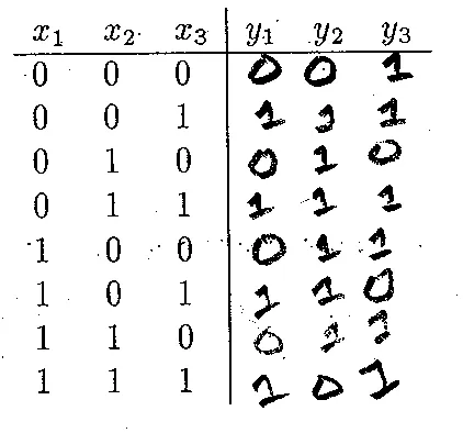
- Each output word. Because the selected row’s devices make 0s and every other column stays 1: 000 → 001; 001 → 111; 010 → 010; 011 → 111; 100 → 011; 101 → 110; 110 → 011; 111 → 101.
FN12-10d read row by row (new figure, computed in the page’s test): each row’s output word at its right end. A device on the selected row pulls its column to 0, and every other column stays 1. Under the columns, each output as a function of the input.
Check. By counting: 8 devices, and the table has 8 zeros. By the columns’ functions, read independently down each column: has devices on rows 000, 010, 100, 110, the rows with , so , and the table’s column reads 0, 1, 0, 1, 0, 1, 0, 1. is 0 only at 000 and 111, where all three inputs are equal: . is 0 only at 010 and 101, where the bits alternate. All three agree with the table, entry by entry.
Answer:
| 0 | 0 | 0 | 0 | 0 | 1 |
| 0 | 0 | 1 | 1 | 1 | 1 |
| 0 | 1 | 0 | 0 | 1 | 0 |
| 0 | 1 | 1 | 1 | 1 | 1 |
| 1 | 0 | 0 | 0 | 1 | 1 |
| 1 | 0 | 1 | 1 | 1 | 0 |
| 1 | 1 | 0 | 0 | 1 | 1 |
| 1 | 1 | 1 | 1 | 0 | 1 |
(.)
Remember. A decoder-driven ROM is read one row at a time: find the input’s row from the bubbles, then every device on that row is a 0 and every empty column is a 1. Count the devices against the zeros.
The key’s table (FN12-10d, p17, the key’s handwriting)
The answer key agrees
Harder variations: addressing and decoders
You need
The split (Chapter 18 §10). , with .
Predecoding (Chapter 19 §11). bits in groups of : lines; each decoder takes inputs; each line feeds decoders.
A ROM (Chapter 19 §11). A full decoder selects one row; a device at (row, column) pulls the column to 0; empty columns stay 1.
These variations added go beyond FN10-10 and FN12-10d: Variation 3 chains the address split into the predecoder, the column selects and the array’s shape, then asks which shape reads faster, a question no past paper asks; Variation 4 runs the ROM backwards, from a function to its devices, and then asks what a fault does. No key exists, so there is no key verdict.
Variation 3: a 16k × 32 memory, from address to array (about 20 minutes)
Variation 3: a 16k × 32 memory, from address to array
added The question. A memory is bits. (a) How many address bits? (b) It is built as one array of 512 rows by 1024 columns: give the row bits, the multiplexer’s ratio and the column bits. (c) The rows are predecoded in 3-bit groups: how many predecoded lines, how many inputs per race NOR, and how many race NORs does each line drive? (d) How many column-select lines are there, and how many multiplexer NFETs does each gate (one on bit and one on per column)? (e) The alternative is 1024 rows by 512 columns. Give its split. With FN10-5b’s column (250 fF per 256 rows, two 1 µm NFETs), which array’s bitline is faster, and by how much?
Hint
What it asks. The whole addressing chain for one memory, then a choice between two shapes judged by the bitline.
The idea. The address bits come from the word count alone; the shape decides only how they divide. The row bits feed the predecoder, the column bits a one-hot decode that drives the multiplexer. The shape also sets the bitline’s length: more rows mean longer bitlines, and the bitline is the largest term of the access (FN10-5c).
Why this formula. ; the predecode counts; .
- Where it comes from. Chapter 18 §10, Chapter 19 §11, and FN10-5b’s gain with the bitline’s capacitance in proportion to its rows (this variation’s assumption).
- Conditions. Every count a power of two, and ; the bitline’s capacitance grows with its rows, since its wire and its cells’ drains both do.
- The tempting alternative. Column bits as : the multiplexer picks a 32-bit word, not a column, and bits would name every single cell.
Variation 3
- (a) Address bits. Because 16k words: 14 bits. The memory has cells.
- (b) The 512 × 1024 split. Because , the array holds it. Rows: bits. Words per row: , a 32:1 multiplexer, column bits. .
- (c) The predecoder. Because 9 bits in 3-bit groups make 3 groups of 8 lines: 24 lines; each race NOR takes 3 inputs, and each line drives of the 512.
- (d) The column selects. Because the 5 column bits are fully decoded, there are one-hot selects. Each picks one 32-bit word, 32 columns, with an NFET on bit and on : 64 NFETs per select.
- (e) The other shape. Because 1024 rows need 10 bits, and words per row give a 16:1 multiplexer and 4 column bits (). Its bitlines span 1024 rows: fF, , against 512 rows’ 500 fF, . The 512 × 1024 array’s bitline is twice as fast.
Variation 3’s two shapes for cells, to scale (new figure): 512 × 1024 with a 9-bit row decoder and a 32:1 multiplexer on 5 bits, and 1024 × 512 with 10 bits and 16:1 on 4. The bitline spans the rows: 512 rows take , 1024 rows (at FN10-5b’s 250 fF per 256 rows).
Check. Both splits add to 14, and both arrays hold cells. The bitline ratio is the row ratio, 2, as the gain’s proportion to says.
Answer: (a) 14 bits. (b) 9 row bits; 32:1; 5 column bits. (c) 24 lines; 3 inputs; 64 race NORs per line. (d) 32 selects, 64 NFETs each. (e) 10 row bits, 16:1, 4 column bits; its bitline takes against : the wider, shorter array reads twice as fast at the bitline.
Remember. Fix the address bits from the word count first; then each shape is a different split of the same bits. Fewer rows, shorter bitlines: column multiplexing is what lets a designer choose them. The price is on the word line: 1024 columns put twice as many access gates on it as 512, so its driver’s gain about doubles, a few against the the bitline saves.
Variation 4: programming the ROM, and a fault (about 20 minutes)
Variation 4: programming the ROM, and a fault
added The question. FN12-10d’s decoder is kept, and its ROM is reprogrammed to output the Gray code of its input: , , . (a) Write the table. (b) Where do the devices go, and how many are there? (c) Pseudo-NMOS columns draw static current while they are pulled low: on average over the eight inputs, how many columns conduct, against FN12-10d’s ROM? (d) A fault holds one decoder output low for good. If it is row 101, which input reads wrong? If it is row 000? (e) Which column can be removed, and how many devices does that save?
Hint
What it asks. The reverse of FN12-10d: from a function to the device grid, then two engineering questions, power and testing.
The idea. A device is a 0, so programming a ROM means placing a device at every 0 of the table. A stuck-low row line deselects its row, so its input sees no devices and reads all ones: the fault shows only if that row had at least one device.
Why this formula. exactly when a device sits at (row , column ), read backwards: a device at every 0.
- Conditions. As in FN12-10d: the full decoder raises exactly one row, and each NFET beats its column’s always-on PFET.
- The tempting alternative. A device at every 1, the “programmed bit” reading. In this ROM a device pulls its column low, so that grid would output the complement of the Gray code.
Variation 4
- (a) The table. Because , , : 000 → 000, 001 → 001, 010 → 011, 011 → 010, 100 → 110, 101 → 111, 110 → 101, 111 → 100.
- (b) The devices. Because a device makes a 0, put one at every 0: row 000 on , , ; 001 on , ; 010 on ; 011 on , ; 100 on ; 101 none; 110 on ; 111 on , . That is devices.
- (c) Static current. Because each 0 is a column pulled low against its PFET, the average is the zeros per input, columns; FN12-10d’s ROM has 8 devices, .
- (d) A stuck row. Because a dead row selects nothing, its input reads 111. Row 101 has no devices and should read 111 anyway: the fault is invisible to every input. Row 000 has three devices: input 000 reads 111 instead of 000.
- (e) A spare column. Because is an input itself, the column can be a wire: its 4 devices (rows 000–011) go, leaving 8.
Variation 4’s Gray-code ROM on FN12-10d’s decoder (new figure, computed in the page’s test): a device at every 0 of the table, 12 in all, and each row’s word at its right end.
Check. By columns: each output is a balanced function (, and are each 0 on exactly 4 of the 8 inputs), so each column carries 4 devices, , as the row-by-row count found. And a Gray code changes one bit between neighbours: 000, 001, 011, 010, 110, 111, 101, 100 does.
Answer: (a) 000, 001, 011, 010, 110, 111, 101, 100. (b) A device at every 0: 12 devices (3, 2, 1, 2, 1, 0, 1, 2 by row). (c) 1.5 columns on average, against 1 for FN12-10d’s ROM. (d) Row 101: no input reads wrong (it has no devices); row 000: input 000 reads 111. (e) , a wire from ; 4 devices saved, 8 left.
Remember. Program a NOR ROM by its zeros. A dead row line is caught only by an input whose row holds a device: a test must exercise every row that has one.
How to approach a dynamic row decoder question
Recognize it by the picture: per word line, a dynamic NOR of address lines with a PFET and a foot on , feeding a second stage footed on and an inverter to the word line; a column with precharge PFETs and write devices; given waveforms for phi1, phi2, the address, write and data_in. The words: “dynamic decoder”, “race”, “nonoverlap window”, “find the waveforms at …”.
The model. The decoder is Chapter 19’s race-based NOR (§12). Stage 1 precharges its node high while is high and evaluates from the moment falls: on every row but the selected one, some input is high and falls. Stage 2 waits for : on the selected row is still high, so stage 2’s node falls and the inverter raises the word line. The column precharges both bitlines on ; in the write devices pull one bitline low (a write), or the selected cell pulls down the bitline on its 0 side (a read); a detector watches one side.
Why it, and its conditions. Derive it from the edge-by-edge picture (Chapter 19 §12). Stage 1’s node drives stage 2’s NFET directly, a precharged-high node into a dynamic gate: Chapter 11’s race (§5). Every row’s starts high; on an unselected row it is on its way down. If stage 2’s foot opens while that is still high, starts to fall on a row that must stay off: a glitch on a wrong word line, which can corrupt a read or write the wrong cell. Stage 1 starts at and stage 2 at , so the gap between them must cover stage 1’s evaluation.
The moves.
- Read each decoder’s inputs and find which row the given address selects (exactly one).
- Phase by phase: precharge ( high), the gap, high, the second gap. Ask in each: which devices are on?
- The word line: up from ; down when stage 2’s precharge PFET turns on (on it falls with ; on it stays up until rises).
- The bitlines: high in precharge; in , a write pulls one low (which one depends on data_in); a read lets the cell pull its 0 side low.
- The detector: trace its polarity from the side it hangs on.
- The clock condition: covers every evaluation between and .
Decide on the way: which clock stage 2’s PFET is on (it sets when the word line falls); which bitline the write pulls for the given data; which side the detector reads.
Traps. Letting the word line fall with when stage 2’s PFET is on . Assuming data_out equals data_in: trace it. Stating the criterion on the wrong gap (the one after falls). Reading the scan’s decoders without the hidden bars.
FN17-6: the dynamic row decoder and its column (about 16 points)
You need
The race-based NOR (Chapter 19 §12). Stage 1: a dynamic NOR of the address lines, precharged by a PFET and footed by an NFET, both on : precharge while is high, evaluate from ; its node stays high only if every input is low. Stage 2: an NFET gated by and a foot on ; its node falls in if is high. An inverter from drives the word line.
The column (Chapter 19 §7, §8). Precharge PFETs on pull and to while is high. A write pulls one bitline to ground through a stack enabled by and write; the cell, opened by its word line, takes that value. A read lets the cell pull down the bitline on the side that holds 0, slowly; the other stays high.
Two phases (Chapter 19 §6, Chapter 14 §3). and are high in turn, never together; between them both are low: the non-overlap gaps.
The question (FN17-6, p13, in the paper’s words). Nearly all of you designed and implemented static row decoders for your SRAM array in the design project. Many of you found that these were pretty big (lots of pFETs) and difficult to pitch match in layout to the SRAM array. Some groups decided to implement this with a more area-efficient dynamic decoder, similar to that shown below. We show only one column of the SRAM.
FN17-6’s decoder and column (Final 2017, p13, redrawn; T bars are ). Four race-based NORs, staggered in two columns as printed. Stage 1 is precharged and footed on (node ). Stage 2’s PFET is on the same line, and its NFET is gated by and footed on (node ). An inverter drives the word line. † The bars on at W0 and W2 lie under drain wires on the scan; they are drawn as the only reading that gives four distinct rows (see Reading the figure). The names and are this guide’s. Right: the column, precharged on , with four 6T cells, the two write stacks and the read inverter from to data_out.
The exam’s own figure (FN17-6, p13)
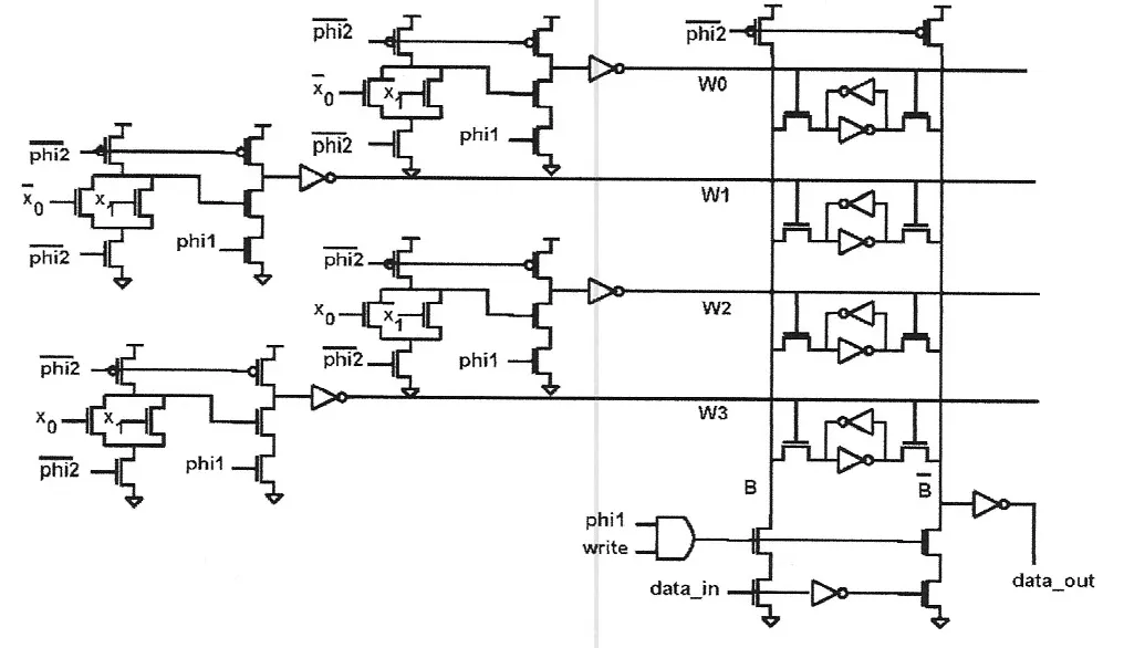
Reading the figure. Each decoder is the race-based NOR with one change from the lecture’s: stage 2’s PFET is gated by the line, not , so is restored only when rises (Chapter 19 §12, the variant). The column’s write stack on conducts when , write and data_in are all 1; the stack on when , write and are. data_out is an inverter on . The decoders’ inputs read W0 = NOR(, ), W1 = NOR(, ), W2 = NOR(, ), W3 = NOR(, ): W1’s and W3’s labels are clear, and the bars on at W0 and W2 lie under drain wires. Only this reading gives four distinct rows, one per address; with W0 = NOR(, ) it would duplicate W1 and no row would answer .
Part (a): the waveforms (8 points)
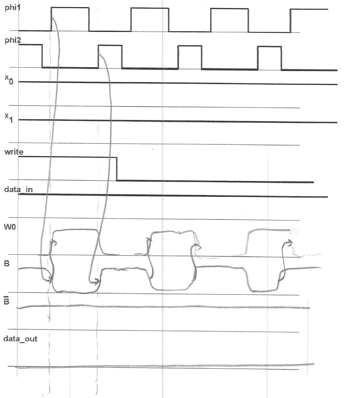
FN17-6a, p15. For the input waveforms shown, find the waveforms at , , , and data_out. (8 points; the value is overwritten on the scan and uncertain)
FN17-6a’s inputs (Final 2017, p15, redrawn; a sketch with no time axis): the paper’s six input rows and the four rows the question asks you to fill. The clock edges are as measured on the scan; write falls late in the second pulse. The scan, which carries the key’s answer, is folded under the answer below.
Hint
What it asks. Four waveforms, over three and a half clock cycles: the selected word line, both bitlines and the output. The unknowns are which row the address selects, when its word line rises and falls, and what the column does on the write cycle and on the read cycles that follow. “For the input waveforms shown” says the answer is a timing diagram aligned with the given clocks.
The idea. The address never changes (), so the same row is selected in every cycle: W0, the only NOR whose inputs are both complements. Its word line rises with and, because stage 2’s PFET is on , stays up until rises. In the first cycle write is high, so the write stack drives the column; after write falls, every cycle is a read of the cell just written. data_in is 1 throughout, so the write pulls low, and the cell then stores a 0 on its side: each read pulls down again and leaves high. data_out inverts .
Why this formula. No formula; three device rules, each from Chapter 19.
- The decoder’s logic (§12). A row is selected when all its NOR inputs are 0: W0 = NOR(, ) is selected at ; W1 has , W2 , W3 both, so their nodes fall in the gap and they stay off.
- When the word line falls. is restored only by its PFET, gated by : it turns on when rises. Between and , floats low and W0 stays high.
- The column (§7, §8). Precharge on restores both bitlines each time is high. A write stack conducts only in with write = 1; data_in = 1 selects the stack on . In a read the cell pulls down the bitline on its 0 side through its access and pull-down NFETs.
- The tempting alternative. Drawing W0 low when falls, as on the lecture’s board, whose stage 2 precharges on ; this figure’s precharges on .
FN17-6a
- The selected row. Because makes , W0’s NOR has both inputs low and its stays high; W1, W2 and W3 each have a high input, so their falls as soon as falls. W0 is the row, in every cycle.
- W0. Because stage 2’s foot opens at with high, falls and W0 rises just after each rise. Because is restored only when rises, W0 stays high through and the gap after it, and falls just after each rise. It is low through each pulse and the gap that follows.
- and in precharge. Because the precharge PFETs are on while is high, both are at during every pulse, and they float high through the gap before .
- The first cycle, a write. Because , write and data_in are all 1 in the first pulse, the stack on conducts and pulls low quickly; ‘s stack has and stays off. W0 is up, so the cell takes ‘s 0 on its side and 1 on its side. stays low (the cell holds it) until rises and precharges it.
- The later cycles, reads. Because write falls during the second pulse, the next pulses read the cell: W0 opens it, and its -side 0 pulls down through the cell’s two NFETs, a slower fall than the write’s. sees the cell’s 1 and stays high. is restored at each rise.
- data_out. Because data_out is an inverter on , and stays high in every phase, data_out stays low throughout.
| Interval (each cycle) | W0 | data_out | ||
|---|---|---|---|---|
| high (precharge) | low | high | high | low |
| gap, to | low | high (floating) | high | low |
| high | rises | falls (cycle 1: write, fast; later: read, slower) | high | low |
| gap, to | high | low | high | low |
| next | falls | restored high | high | low |
The FN17-6a answer on the paper’s inputs (new figure; the levels come from the page’s phase-by-phase logic trace, the slopes are a sketch). W0 rises just after each rise and falls just after the next rise. falls steeply in the first (W, the write: a stack pulls it) and more gently in the later ones (R, reads: the cell pulls it). It is restored at each rise. stays high and data_out low. Dotted guides: the and rises.
Check. By a logic-level simulation of the four decoders and the column, phase by phase over three cycles (the page’s test): W0 is the only word line that ever rises, it is high exactly in and the gap after it, is low in the same intervals, and data_out never change. By the polarity rule of Chapter 19 §8: this column puts the data on the side as a 0 (data_in = 1 pulls low), and the read inverter on reports the side, so data_out is the complement of data_in, 0 here, as found.
Answer: W0 is selected (the only NOR with both inputs, and , low). W0 rises after each rise and falls after the next rise (high through and the gap after it). : high in each precharge; pulled low in the first (the write of data_in = 1), then discharged by the cell in each later (reads), and restored high at each rise. : high throughout. data_out: low throughout. (Before the first write the cell’s state is unknown; if it held the opposite value, could dip briefly at the start of the write until the cell flips.)
Remember. Find the selected row from the NOR inputs first; then go phase by phase. The word line falls when stage 2’s precharge PFET turns on, so read its clock. A write is fast (a stack pulls the line); a read is slow (the cell pulls it). Trace the detector’s polarity: here data_out is the complement of data_in.
The key’s answer (FN17-6a, p15, the key’s handwriting)
The answer key agrees
Part (b): the non-overlap criterion (8 points)
FN17-6b, p16. What criterion does the dynamic decoder put on the nonoverlap window of phi1 and phi2? (8 points)
Hint
What it asks. A timing condition, in words and as an inequality, on the gap between the two clocks, and why the decoder needs it. “Criterion” asks for the condition; the marks are for naming the gap and the delay it must cover, and the reason.
The idea. Stage 1 of every decoder is precharged high and starts to evaluate when falls; on every unselected row its node is falling. Stage 2 opens when rises, and it fires on any row whose stage-1 node is still high. If an unselected row’s node has not yet fallen, that row’s word line starts to rise too: two rows on one column. So the gap from to must be long enough for stage 1 to finish evaluating.
Why this formula. of the stage-1 NOR.
- Where it comes from. The race-based NOR feeds a precharged-high node directly into a dynamic gate: the race of Chapter 11 §5. Domino would put an inverter between them; this circuit removes the race with the clock instead (Chapter 19 §12). The lecture: “I can twiddle the phi one, phi two bar relative to the phi one to ensure that this guy evaluates before this guy evaluates” (Lecture18, 57:19–57:49).
- Conditions. is the slowest unselected row’s: a single input high (one NFET in series with the foot) discharging and stage 2’s gate. The address must be stable before falls; anything else that evaluates on ahead of the NOR adds its delay.
- The tempting alternative. Putting the condition on the other gap, to . Nothing races there: in this circuit the word line simply stays up through it.
FN17-6b
- When stage 1 starts. Because its foot is on , every decoder’s stage 1 starts to evaluate at ; unselected rows’ begin to fall.
- When stage 2 starts. Because its foot is on , stage 2 starts to evaluate at , and it pulls down on every row whose is high at that moment.
- The race. Because an unselected row’s needs to fall, if rises sooner, that row’s starts to discharge, and a dynamic node that falls cannot come back up until it is precharged: the row’s word line glitches or rises, and two cells drive the column at once.
- The criterion. Because the gap is the time stage 1 has alone: , from falling to rising, must exceed the stage-1 NOR’s evaluation time, with margin for clock skew.
Check. By the limit (Chapter 19 §12, its Check): stage 2 opens while every unselected is still high, so every word line would start to rise at once. By the selected row: its never falls, so the criterion costs it nothing but waiting; the gap is time the decoder uses, not lost.
Answer: The non-overlap window from falling to rising must be longer than the evaluation time of the decoder’s stage-1 NOR: . Every unselected row’s stage-1 node must have fallen before opens stage 2’s foot; otherwise stage 2 sees a still-high node, discharges on a wrong row, and raises a second word line (the race of a dynamic node driving a dynamic gate).
Remember. A race-based NOR trades domino’s inverter for a clock gap: ( to ) everything that evaluates on before the clock-qualified stage.
The answer key agrees
Harder variations: the dynamic row decoder
You need
The decoder and the column (FN17-6). W0 = NOR(, ), W1 = NOR(, ), W2 = NOR(, ), W3 = NOR(, ); a row is selected when both its inputs are 0. Its word line rises at and falls at . A write in pulls low if data_in = 1, low if data_in = 0; a read lets the cell pull down its 0 side; data_out .
The clock condition (Chapter 19 §12). of every stage between and ; FN10-5’s path: stages I–III before (13.99 ), IV–V after it (7.58 ).
These variations added are harder than FN17-6: Variation 5 changes the address and the data every cycle and asks what the column returns, a longer trace with a surprise in it; Variation 6 turns FN10-5’s decode path into a clock budget in picoseconds, heavy arithmetic against the clock. No key exists, so there is no key verdict.
Variation 5: four cycles at two addresses (about 20 minutes)
Variation 5: four cycles at two addresses
added The question. FN17-6’s circuit runs four cycles. Cycle 1: write data_in = 0 at . Cycle 2: write data_in = 1 at . Cycle 3: read at . Cycle 4: read at . The address and write change only while is high. (a) Which word line rises in each cycle? (b) In each , which bitline falls, and what is data_out? (c) Compare what is read with what was written. (d) Change one connection so data_out returns the data written. (e) Over which interval must the address be stable, and why is it changed while is high?
Hint
What it asks. FN17-6a’s trace over a sequence the paper does not use: two rows, both data values, writes then reads, and then what the polarity means for the design.
The idea. Each cycle is FN17-6a’s analysis with its own row and data. The column’s polarity is fixed by the wiring: data_in = 1 pulls low, a 0 on the cell’s side; the detector reads and inverts it, which reports the side’s value. So the column returns the complement of what it was given, and only a trace through both values shows it.
Why this formula. The three device rules of FN17-6a (selection by NOR, word line from to , the write stacks and the read through the cell), and dynamic-gate input monotonicity (Chapter 11 §5): a dynamic gate’s inputs may only fall during evaluation, never rise.
Variation 5
- (a) The rows. Because a row needs both NOR inputs at 0: (, ) zeroes and , the inputs of W1; zeroes and , W2’s. So W1, W2, W1, W2.
- (b) Cycle 1, write 0 into W1’s cell. Because data_in = 0 enables the stack on , is pulled low and stays high; the cell stores 1 on its side. data_out = = 1 during this .
- (b) Cycle 2, write 1 into W2’s cell. Because data_in = 1 enables the stack on , falls, stays high; that cell stores 0 on its side. data_out = 0.
- (b) Cycle 3, read W1. Because W1’s cell holds 0 on its side, it pulls down; stays high; data_out = 1.
- (b) Cycle 4, read W2. Because W2’s cell holds 0 on its side, falls, stays high; data_out = 0.
- (c) Read against written. Because the reads give 1 where 0 was written and 0 where 1 was: data_out is the complement of data_in. FN17-6a wrote only a 1, so its waveforms alone could not tell a complementing column from one whose output is stuck at 0; its Check predicted the complement from the wiring, and two values show it.
- (d) A fix. Because the inverter on reports the cell’s side, and a written 1 puts a 0 there, hang the data_out inverter on instead: data_out is 1 exactly when the cell’s side holds 0, that is, when 1 was written. (Moving the data_in inverter to the stack works too: a written 1 then pulls low.) Either way cycle 3 reads 0 and cycle 4 reads 1.
- (e) The address window. Because stage 1 evaluates from , an input that rises during evaluation would discharge the selected row’s , losing the access, and one that falls cannot recharge an unselected row’s , which has already fallen: the new row would never rise. Because stage 2 evaluates only while is high (its foot), the selected row’s must stay high until falls. So the address must be stable from to . After falls, stage 2’s foot is off and only floats low until rises, so a change in that gap no longer reaches the word line, but any skew between the address and ‘s fall eats straight into it. While is high, stage 1 precharges with its foot off and nothing evaluates: that is the safe time to change the address.
Variation 5’s four cycles (new figure, from the page’s logic trace; the slopes are a sketch). Cycles 1 and 2 write 0 into W1’s cell and 1 into W2’s; cycles 3 and 4 read them back. The address and the controls change only while is high, and data_in is unused (hatched) in the reads. data_out reads 1, then 0: the complement of what was written.
Check. By the test’s phase-by-phase simulation: word lines W1, W2, W1, W2; (, ) in : (1, 0), (0, 1), (1, 0), (0, 1); data_out 1, 0, 1, 0; and with data_out taken from , the reads give 0 then 1. By Chapter 19’s Memorize line: “data on the bit side, so a read through the inverter on returns the complement of the data written” (On the exam).
Answer: (a) W1, W2, W1, W2. (b) Cycle 1: falls, data_out 1; cycle 2: falls, 0; cycle 3: falls (read), 1; cycle 4: falls (read), 0. (c) The reads return the complement of the writes (1 for 0, 0 for 1). (d) Take data_out from an inverter on (or move the data_in inverter to the other stack). (e) Stable from (stage 1 starts to evaluate) to (stage 2 stops): a dynamic gate’s input must not rise during evaluation, and a fallen node cannot recover. Nothing evaluates while is high, so precharge is the safe time to change it; the gap after would also miss the word line, but with no margin for skew.
Remember. Trace both data values before trusting a column’s polarity. A dynamic decoder’s address must be stable from its first stage’s evaluation to the end of its last; precharge is the safe time to change it.
Variation 6: the decode path as a clock budget (about 25 minutes)
Variation 6: the decode path as a clock budget
added The question. FN10-5’s decode path is clocked as the lecture’s race-based NOR: stages I–III evaluate between and , stages IV–V after , and the word line falls with . Take ps, for example. The column senses at 100 mV (FN10-5’s column at 2.5 V: ), and the sense amplifier needs to regenerate (for example), all inside . Precharge needs high for (for example). (a) The minimum , in ps. (b) The minimum high time. (c) The minimum period, with no second gap, and the frequency. (d) Redo (a) and (c) with the topology’s fan-out of 64. (e) A clock generator gives a 50 % duty cycle: the precharge and the first gap form one half, the other. What period now? (f) What share of the period (c) is the gap?
Hint
What it asks. The FN10-5 numbers placed on a clock: three intervals, each with its own content, then their sum, with the arithmetic that an exam under time pressure asks for.
The idea. A cycle is precharge, then the gap, then . The gap must hold the stages that evaluate on (the race condition); must hold everything from the clock qualification to the sensed data. Each interval is a sum of gains times ; the period is their sum. A fixed duty cycle wastes whatever the shorter half does not need.
Why this formula. ; ; .
- Where it comes from. The race condition (FN17-6b) and FN10-5’s gains; the bitline’s swing time in proportion to (Chapter 19 §7).
- Conditions. The word line falls with (the lecture’s stage 2 on ), so the sensing must end inside ; the second gap is taken as zero.
Variation 6
- (a) The gap. Because stages I–III must finish before opens stage IV: , so ps.
- (b) ‘s high time. Because IV, V, the bitline’s 100 mV and the regeneration all happen while is high: ps.
- (c) The period. Because precharge, gap and access follow each other: ps, 771 MHz.
- (d) Fan-out 64. Because only stage II changes, to 1.71: the gap is ps, and the period ps, 874 MHz.
- (e) A 50 % duty cycle. Because each half must hold the larger of its two needs, precharge plus gap ( ps) or (577 ps): each half is at least 720 ps and the period ps, 142 ps longer than (c) (from the unrounded times).
- (f) The gap’s share. Because the gap is 420 of 1297 ps: 32 % of the period goes to the race condition, the price of removing domino’s inverter.
Variation 6’s cycle at ps (for example; new figure, computed): precharge, 300 ps while is high (hatched); stages I–III (115, 205 and 100 ps) in the gap, ps; stage IV, stage V, the bitline’s 100 mV swing (BL) and the sense amplifier’s regeneration (SA) while is high, 577 ps. Period 1297 ps.
Check. By (a) + (b) against FN10-5a: the gap and the access stages hold all five gains, , and the period minus precharge, ps, is at 30 ps (997 ps): the cycle is the access time plus precharge. By size: at ps an FO4 is about 90 ps, so the 1297 ps cycle is 14.4 FO4, inside FN10-5c’s 12–15 FO4 cycle, as Variation 2 found for a sensed array.
Answer: (a) ps. (b) high ps. (c) ps (771 MHz). (d) ps; ps (874 MHz). (e) 1440 ps. (f) 32 %.
Remember. Split a clocked memory’s cycle by what each interval must hold: precharge in , the race in the gap, the access in . The gap is set by the decoder’s front stages: shrink the predecoder’s fan-out, and the gap shrinks.