F1. Past finals: devices
The finals open with device short answers: a few sentences, sometimes one line of arithmetic, on why the threshold moves, how much a transistor leaks, what the body effect does to a gate, and what sets a delay. This page re-solves every such part of the four past finals that the midterm material covers, grouped by family, newest exam first. The midterm asks the same kind of question (MT17-1b–c, MT21-2; see M3), so these are extra practice for the same points.
Every number below is re-solved here and checked in this page’s review/examples.check.ts; none is copied from a key. Where a key disagrees or leaves something out, the folded note on the key at the end of the part explains it, and the table at the end lists them all. The 2019 final has no key: its parts are solved independently, with no other solution shown.
After this page you can:
- explain DIBL, threshold roll-off and inverse roll-off from the share of the bulk charge the gate controls;
- say which way the threshold moves with the oxide thickness, and why;
- turn a current-defined threshold into decades of leakage, with the source raised or in a stack;
- say which edge of a gate the body effect slows, and by about how much;
- explain why FO1 is more than a quarter of FO4;
- find how sensitive a delay is to the supply, for a velocity-saturated and a square-law device.
Before you start
How to use this page. Each part is restated with its source page (FN12-1b, p3 is the Fall 2012 final, question 1b, physical PDF page 3) and its points, and shows the exam’s figure where it has one. The threshold family opens with a short How to approach section: how to recognize the question, the moves in order, why the formulas apply, and the traps. The other families use the midterm page’s approach sections, and each one’s first part links them. Then every part is worked the same way: what it asks, the idea behind the method, the solution in steps (each step gives its reason first), a check on the result, the answer, and one thing to remember. Try each part on your own first; open the Hint if you are stuck, and step through the solution before you press “Show all”. The answer key’s verdict is folded at the end of each part. The chapters teach each method in full, and every solution links the section.
| Family | Parts (newest first) | Points | Chapters |
|---|---|---|---|
| The threshold: short channels and the oxide | FN19-2a, 2b, 2c (partial), FN17-1a, FN17-1c | 30 + 10 | 3, 4 |
| Subthreshold leakage: a defined threshold, a raised source, a stack | FN12-1a–c | 18 | 4, 5, 7 |
| The body effect in a shifted-supply inverter | FN10-1 | 10 | 5 |
| Delay as charge over current: FO1, FO4 and the supply | FN12-2, FN10-6a–b | 6 + 20 | 4, 5 |
The rest of these questions is on later topics and left out: FN17-1b, 1d and 1e (decoupling capacitance, clock latency, infant mortality) and FN10-6c–d (clock jitter and hold failure).
Conventions.
- An NFET’s threshold falls when the gate has less bulk charge to hold: (Chapter 3, Section 8). For a PFET read .
- Subthreshold current changes tenfold per millivolts of : (Chapter 4, Section 11). The course treats it as independent of once DIBL is ignored.
- A delay is charge over current: (Chapter 5, Section 11). Chapter 7’s is a fitted constant with no supply dependence, so supply questions go back to the currents.
How to approach a threshold question
Recognize it by its wording. The question names a change to the device or to how it is wired (a higher , a shorter channel, halo doping, a thinner oxide, a source above the body) and asks “why is this?” or “how does vary with …?”. There is rarely a number to compute: the points are for a cause-and-effect chain of three or four sentences. FN19-2 carried 30 points, FN17-1a and 1c 10 together, and FN10-1 10. FN12-1c leans on the same reasoning.
The moves, in order.
- Write the threshold: . Every answer in this family comes out of one of its terms.
- Name the term the change touches. The drain or the source taking a share of (DIBL, roll-off); the body doping, through and (halos); , through ; , through (the body effect).
- Say which way it moves, as a chain. “A wider drain depletion region holds part of the charge, so the gate holds less, so falls, so falls.” Each link needs its because.
- Say what that does to the device: its current, its delay or its leakage. A lower means more overdrive and more leakage; a higher one, less of both.
Why these formulas.
- The threshold. At threshold the gate voltage is split into three parts: , the offset from the gate’s and the silicon’s work functions; , the band bending that inverts the surface; and , the voltage across the oxide needed to hold the depletion charge under the gate. The oxide is a capacitor, per unit area, and . The formula holds for a uniformly doped body at the strong-inversion criterion, measured from the gate to the source (Chapter 3, Section 8).
- The bulk charge. is the charge of the depletion region under the gate. It grows as with the doping and with a source-to-body reverse bias (Chapter 5, Section 1). In a short channel the source’s and the drain’s depletion regions reach under the gate and hold part of that charge themselves, so the gate has less to hold (Chapter 4, Section 12).
- What the device does with it. Above threshold the current depends on the overdrive : in proportion when velocity saturated (Chapter 4, Section 7), as its square in the long-channel square law (Chapter 4, Section 4). Below threshold it falls one decade for every millivolts below (Chapter 4, Section 11).
Decisions to make on the way. NFET or PFET: for a PFET, read and , and remember that its body is the n well. Then each device’s own and , measured from its own source, not from ground.
Traps. “The gate has full control of the bulk charge” (FN17-1c’s key): the oxide thickness doesn’t change , only the voltage needed to hold it. Comparing absolute voltages instead of each device’s and (FN10-1’s circuit runs from 2.5 to 5 V). Adding to itself: it enters only under the root. A direction with no because.
1. The threshold: short channels and the oxide
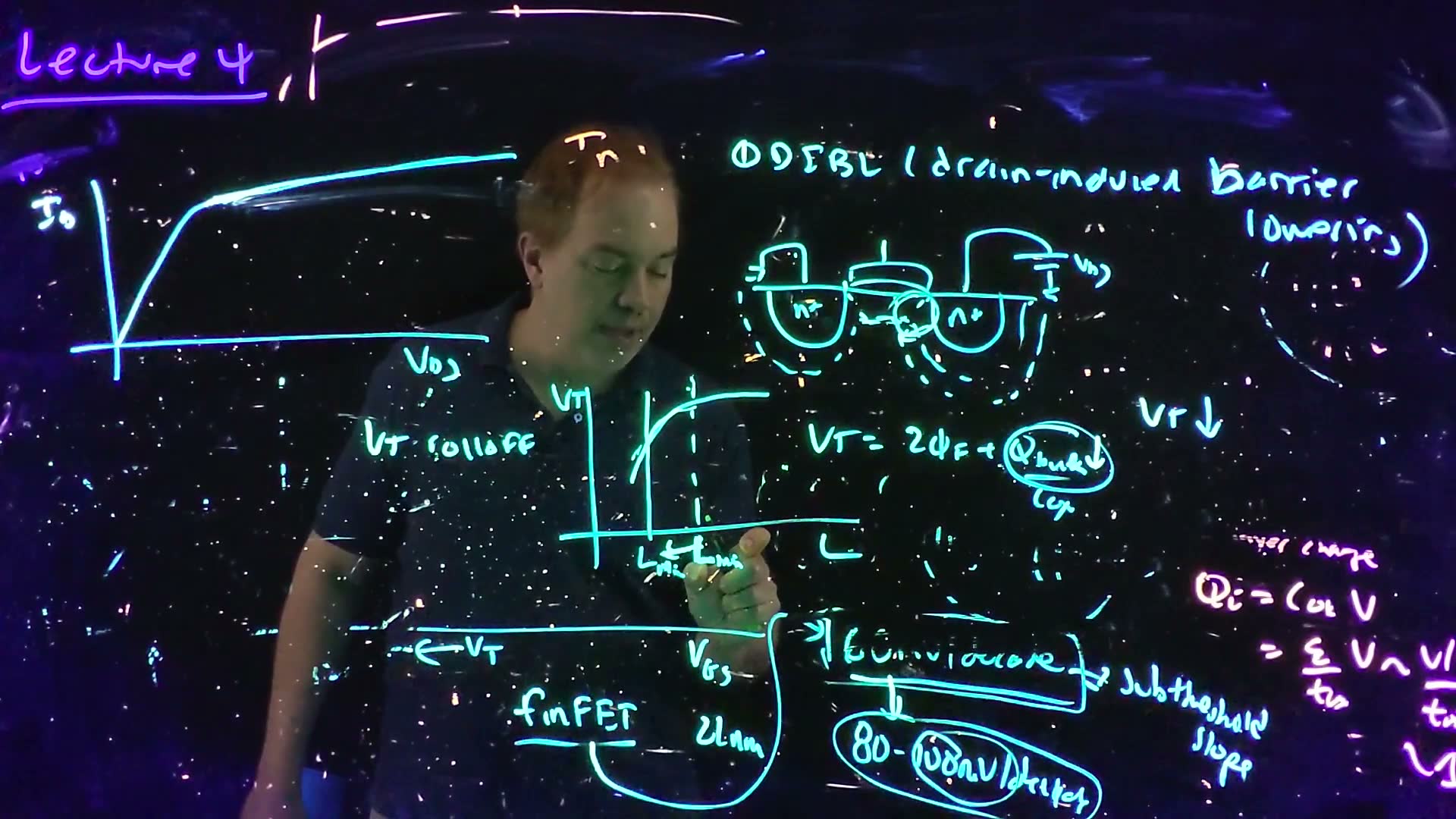
FN19-2a: the threshold falls as VDS rises
FN19-2, p5 (Fall 2019). Consider short-channel effects. Remember that device is strongly affected by bulk charge under the channel.
(a) (10 points) One typically finds that the magnitude of the threshold voltage of a short-channel device decreases with increasing . Why is this?
Hint
What it asks. Why a short transistor’s threshold falls when its drain voltage rises. The words “short-channel” and the stem’s “bulk charge under the channel” decide the method: an argument about who holds the depletion charge under the gate.
The idea. The gate must hold all of through the oxide, and that sets the threshold’s term (How to approach). The drain is a reverse-biased junction, so its depletion region widens as rises (Chapter 3, Section 4). Depletion widths didn’t shrink with the channel length, so in a short device the drain’s region reaches under the gate and holds part of the charge there. This is charge sharing, and it is how Lecture 4 explains every short-channel effect (Chapter 4, Section 12). The long-channel picture, in which doesn’t depend on at all, can’t explain the effect.
DIBL
- Start from the threshold. Because the stem points at the bulk charge, write . The gate must support all of through the oxide (Chapter 4, Section 12).
- The drain’s depletion region grows. The drain is a reverse-biased junction, so raising widens its depletion region (Chapter 3). Depletion widths did not scale with the channel, so in a short device that region reaches under the gate (64:30).
- The gate holds less. Because the drain now holds part of the depletion charge under the channel, the gate controls less of it: in the formula falls (64:58–65:24).
- So the threshold falls. A smaller gives a lower , and more so the higher . This is drain-induced barrier lowering, DIBL. (For a PFET read and .)
- Why only short devices. In a long device the drain’s depletion region is a small part of the channel, so its share is negligible: DIBL is a short-channel effect.
Check. The long-channel limit. As grows, the drain’s share of the charge under the gate goes to zero, and stops depending on : the flat saturated current of the long-channel I–V (Chapter 4, Section 4). The effect has the right sign too: the board’s I–V (top left) keeps rising in saturation, as a falling requires.
Answer: DIBL. A larger widens the drain’s depletion region, which takes over part of the bulk charge under the gate; the gate has less to hold, so falls.
Remember. A short-channel question is charge sharing. Say who else holds part of , and the threshold falls with it. With DIBL, the drain’s share grows with .
FN19-2b: the threshold falls as the channel shortens
FN19-2b, p5 (10 points). Before the advent of advanced halo doping techniques, one found that circuits with smaller channel lengths had threshold voltage of lower magnitude. Why was this? This is the effect we described in class as “ rolloff.”
Hint
What it asks. Why shorter transistors had lower thresholds before halo doping: “ roll-off”. The variable is now the channel length, at a fixed .
The idea. The charge-sharing argument of (a), with as the variable instead of . The source and the drain have depletion regions even at low , from their built-in voltages, and those regions hold the charge at the two ends of the channel. Their widths are set by the doping and the junction voltages, not by (Chapter 3, Section 3). So what matters is their share of the region under the gate, and that share grows as shrinks (Chapter 4, Section 12).
Roll-off
- The ends of the channel belong to the junctions. Even at low the source and the drain have depletion regions, and they hold the charge at the two ends of the channel (Chapter 4, Section 12, 67:15).
- Their share grows as L shrinks. Their width is set by the doping and the junction voltages, not by . So as shrinks they hold a larger share of the charge under the gate (67:44).
- So the threshold falls. Because the gate is left with less per unit area, falls with : roll-off. The drain, being reverse-biased, has the wider region and contributes the larger part.
- Why it matters (68:13). varies from device to device with lithography. Where is steep, that becomes threshold variation, so is placed where the curve is flat.
Check. The two ends of the curve. At long the junctions’ shares vanish and approaches Chapter 3’s long-channel value, so the curve is flat; at short the shares grow and it falls. That is the shape of the board’s “ rolloff” plot (centre).
Answer: at short the source and drain depletion regions, which don’t shrink with , hold a larger share of the bulk charge under the gate; the gate holds less, so is lower.
Remember. Roll-off is DIBL’s argument with as the variable: regions of fixed width take a larger share of a shorter channel. Put where is flat.
FN19-2c: halo doping and inverse roll-off (partial)
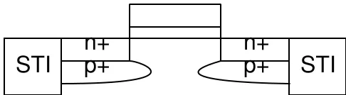
FN19-2c, p6 (10 points). Modern device technologies have introduced halo doping. In this case, the region directly under the source and drain is more heavily doped than the substrate as a whole. This helps control the extent of the source and drain depletion regions. The case of the nFET is shown below. In the presence of halo doping, one generally finds an “inverse” rolloff in which smaller channel lengths lead to higher magnitude threshold voltages. Why might this be?
Partial. Lecture 4 names inverse roll-off, “with some of these more complicated doping tricks” (68:45), and draws it (72:49), but never says “halo” and never says why the threshold rises. The answer below uses only what the course does teach; the picture of halo pockets averaging into the channel’s doping goes beyond the lecture.
Hint
What it asks. With halo doping, shorter channels have higher thresholds: the opposite of (b). Why “might” this be? The word “might” asks for a plausible mechanism, argued from the threshold formula.
The idea. The threshold now rises, so the mechanism must give the gate more charge to hold, not less. The doping is the term to look at: grows as , so heavier doping under the gate raises (Chapter 3, Section 8). The halos are pockets of heavier doping of fixed size at the two ends of the channel. As shrinks they make up more of it, so the doping the gate sees rises added. They also narrow the source and drain depletion regions, which works against (b)‘s roll-off.
Inverse roll-off
- Find the term. Because the threshold rises, look for something that adds charge: the oxide term grows with the body doping, , so rises roughly as (Chapter 3, Section 8). Real devices shape the doping profile to control short-channel effects (Chapter 3, Section 10).
- Long channels see the substrate. The halo regions sit at the two ends of the channel, and their size does not shrink with . In a long device they are a small part of the region under the gate, which sees mostly the substrate’s doping.
- Short channels see the halos. As shrinks, the two halos make up a larger fraction of the channel, and finally they meet. So the doping the gate must deplete, averaged along the channel, rises added.
- So the threshold rises. More doping means more for the gate to hold, so rises as shrinks: inverse roll-off.
- The roll-off is delayed, not gone. Because heavier doping keeps the source and drain depletion regions narrow (width , Chapter 3), they take less of the gate’s charge, and the ordinary roll-off of part (b) sets in later. At still shorter it wins again, and rolls off, as the board’s curve shows.
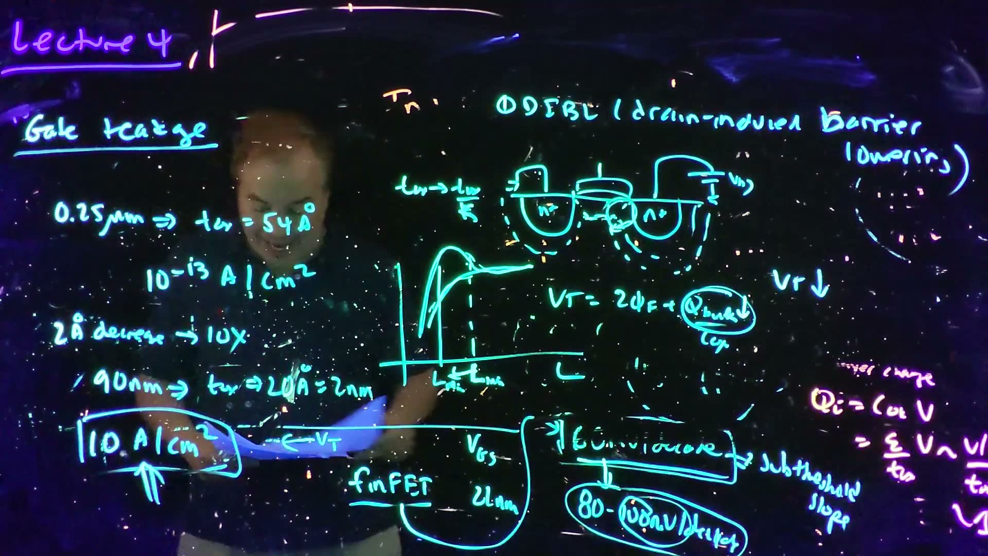
Check. added The steps must reproduce the board’s hump, and in the halo-averaging picture they do. Once the halos meet, a shorter channel can’t raise the average doping any further, while the junctions’ share of the charge keeps growing. So the rise has to stop and turn into a roll-off at the shortest lengths: up first, then down.
Answer: at short the heavily doped halo regions fill a larger share of the channel, so the gate must hold more bulk charge, , and rises; at the same time the halos keep the source and drain depletion regions small, so the charge-sharing roll-off of part (b) sets in only at shorter lengths.
How big? added In Chapter 3’s worked device (), doubling the doping from to raises the oxide term from 0.241 V to 0.348 V and from 0.833 V to 0.869 V. A modest change in the average doping moves by a tenth of a volt or more.
Remember. Ask which way the charge moves. Anything that adds doping under the gate raises ; anything that takes charge off the gate lowers it. With halos, the first wins at moderate lengths and the second at the shortest.
FN17-1a: DIBL against channel length
FN17-1a, p2 (Fall 2017, 5 points). How is drain-induced barrier lowering (DIBL) affected by device channel length? Why? What effect does DIBL have on MOS device characteristic?
Hint
What it asks. Three things in 5 points: how DIBL depends on , why, and what it does to the device’s characteristic (its I–V curves).
The idea. The mechanism is FN19-2a’s: the drain’s depletion region takes a share of the charge under the gate. What this question adds is the approach section’s last move: say what the moved threshold does to the device. In saturation the current depends on the overdrive (Chapter 4, Section 7), so a that falls with gives a current that rises with . Below threshold the current depends on how far is below , so the leakage rises too.
- Shorter channels have more DIBL. Because the drain’s depletion region does not shrink with , it takes a larger share of the bulk charge under a shorter gate (the argument of FN19-2a and 2b).
- The saturated curves slope. Because in saturation the current is set by the overdrive, a higher that lowers raises the overdrive and so raises the current (Chapter 4, Section 12, 66:03–66:42). The saturated curves slope upward: a finite output conductance; the device is no longer a current source.
- The off-state leaks more added. Because the off device has , it has the lowest , and so more subthreshold leakage (Chapter 4, Section 11). This is why FN12-1 and FN19-1 say “ignore DIBL”.
Check. The sign. A lower means more current, so the saturated curves must slope up with , never down; the board’s I–V sketch (top left) slopes up. And in the long-channel limit the slope disappears, as step 1 requires.
Answer: DIBL grows as shrinks, because the drain controls a larger share of the bulk charge; it makes fall with , which gives the saturated I–V curves a slope (lower output resistance) and raises the off-state leakage.
Remember. For “what effect on the characteristic”, follow into the overdrive: a threshold that falls with gives a saturated current that rises with , and more leakage when off.
The answer key agrees
FN17-1c: the threshold against oxide thickness
FN17-1c, p2 (5 points). How does the transistor threshold voltage of an nMOS transistor vary with oxide thickness? Explain.
Hint
What it asks. Which way an NFET’s threshold moves when its gate oxide is made thinner or thicker, and why. “Explain” says that the reason carries the points.
The idea. The approach section’s second move: find the term the change touches. The oxide thickness enters only through , so only the oxide term moves (Chapter 3, Section 8). The oxide is a capacitor that must hold the charge , and a capacitor’s voltage is its charge over its capacitance. The tempting reason, “a thinner oxide gives the gate more control over the bulk charge”, is wrong: is set by the body doping and doesn’t change with . Only the voltage needed to hold it does.
- Write the threshold. Because could enter any of its terms, start from the whole formula: , with (Chapter 3, Section 8).
- Find the term. and depend only on the body doping. Only the oxide term depends on , and it is proportional to it: the oxide is a capacitor that must hold , and a thinner one needs less voltage to do it.
- Say which way. So a thinner oxide gives a lower , a thicker one a higher . In Chapter 3’s device (, ) the oxide term is 0.120, 0.241 and 0.482 V at 2.5, 5 and 10 nm, so is 0.954, 1.074 and 1.315 V.
- What else it does. Because the body effect’s growing term is the same , a thinner oxide also shrinks the body effect (Chapter 5, Section 1).
Check. Only one term moves, so each change in must equal the change in the oxide term: from 5 to 10 nm, and from 2.5 to 5 nm. ✓ Doubling doubles the oxide term each time, as proportionality requires.
Answer: falls as falls (and rises as it grows), because the voltage across the oxide needed to hold the depletion charge, , is proportional to .
Remember. One term at a time. enters only through : a thinner oxide lowers and shrinks the body effect. The doping enters through and .
The answer key differs
It gives the same direction, but its reason, “the gate has full control of the bulk charge”, is loose: does not change with ; the voltage needed to hold it does.
Check yourself A process thins the gate oxide from 5 nm to 2.5 nm and wants to keep VT. Which way must the body doping move?
Up. The oxide term halves (0.241 → 0.120 V in Chapter 3’s device), so must grow to make it up, or must be changed by the gate material (Chapter 3, Section 10).
2. Subthreshold leakage: a defined threshold, a raised source, a stack
FN12-1a: a threshold defined by a current
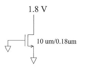
FN12-1a, p2 (Fall 2012, 6 points). If the nFET threshold voltage is defined by a saturated drain current of through a device, what is the threshold voltage of the device above if the drain leakage current is 100 nA? Please ignore DIBL and assume a 80 mV/decade subthreshold slope.
Hint
What it asks. The threshold is defined as the at which the device carries 100 µA in saturation, and at it leaks 100 nA. Find . The words “defined by a saturated drain current” decide the method: this threshold is a point on the current curve, so the gate voltage between it and zero follows from the two currents.
The idea. This is the subthreshold count of M3’s device short answers, run backwards: from two currents to a voltage, instead of from a voltage to a current. Below threshold the current changes tenfold for every millivolts of , (Chapter 4, Section 11). With DIBL ignored, doesn’t change it. Put and solve: . The threshold here is the current-criterion one, , not the physics one (Chapter 4, Section 8).
- Which threshold. Because the question defines it by a current, this is the current-criterion threshold, (Chapter 4, Section 8): with at the supply, is the where the current reaches , i.e. per µm of width.
- Count the decades. The figure’s device has and leaks 100 nA. So from down to 0 the current falls by : three decades.
- Price them in volts. Because the slope is 80 mV per decade, each decade costs 80 mV of (Chapter 4, Section 11), so .
Check. Run it forward. At the gate is 240 mV below threshold, which at 80 mV per decade is three decades: , the leakage the question gives. ✓
Answer: .
Remember. A current-defined threshold turns into decade counting: (decades between the threshold current and the leakage). Always ask which definition of a question uses.
The answer key agrees
FN12-1b: the source raised to 1 V
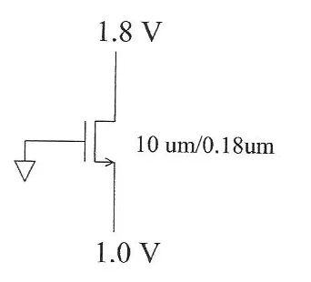
FN12-1b, p3 (6 points). If the source voltage is instead set to 1.0 V as shown below, what is the drain current through the device. Please ignore DIBL and body effect.
Hint
What it asks. The same device with its source raised to 1.0 V, gate at 0 and drain at 1.8 V. “Ignore DIBL and body effect” decides what stays fixed: the threshold stays at (a)‘s 240 mV, and doesn’t matter, so only changes.
The idea. The same decade count as (a). The new point is that is measured from the gate to the source. The gate hasn’t moved, but the source has risen 1 V above it, so the gate is 1 V further below threshold than in (a). Reading “the gate is grounded, as in (a)” and keeping (a)‘s current is the trap of comparing absolute voltages (How to approach). With DIBL ignored, the subthreshold current depends on alone (Chapter 4, Section 11).
- Measure from the source. Because the subthreshold current depends on , gate to source, read both terminals: the gate is at 0 and the source at 1.0 V, so . The drain still sits 0.8 V above the source, which with DIBL ignored changes nothing.
- Count the decades. Because every 80 mV below is another decade, decades below the 100 nA of part (a).
- The current. .
Check. Count from the threshold instead. is below , which is decades below the 100 µA that defines it: . ✓ The same, because (a)‘s three decades plus these 12.5 make 15.5.
Answer: : raising the source by 1 V cuts the leakage by 12.5 decades.
Remember. is gate to source. A source raised above the gate is a reverse gate bias, and every millivolts of it is one more decade of turn-off. Part (c) uses this.
The answer key agrees
FN12-1c: two stacked devices against one
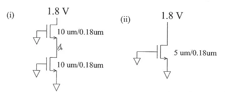
FN12-1c, p4 (6 points). Stacked devices are often used to control subthreshold leakage. Which of the two circuits below could be expected to have the smaller drain leakage current? Explain. Hint: Consider carefully your answer to part (b).
Hint
What it asks. Which leaks less when off: two 10 µm NFETs in series (i), or one 5 µm NFET (ii)? Explain. The exam’s hint points at (b): a raised source. “Explain” carries the points, and this time the question doesn’t say to ignore DIBL or the body effect.
The idea. First make sure the comparison is fair: by the stack rule, transistors in series drive like one transistor of width , so two 10 µm devices drive like one 5 µm device (Chapter 7, Section 8). Then find node A. It is tied to nothing, and the two devices are in series, so it settles where they carry the same current. Then read each device’s own , and from that node, and apply the threshold section’s moves to each. Three effects come out: part (b)‘s negative and the body effect on the top device, and the missing DIBL on the bottom one. Naming only part (b)‘s effect is the tempting answer, and on its own, with the other two ignored, it is not enough.
Stack against single device
- A fair comparison. By the stack rule, two 10 µm devices in series drive like one 5 µm device (Chapter 7, Section 8). So both circuits have the same on-current; the question is their off-current.
- Circuit (ii). Because leakage is per µm of width, one 5 µm device with and the full 1.8 V across it leaks, by part (a), half of the 10 µm device’s leakage, about 50 nA.
- Circuit (i): node A rises. Because the same current must flow through both devices, A can’t stay at 0: there the top device would leak like a full 10 µm device while the bottom one, with nothing across it, could carry none of it. So A charges up until the two currents match, to some voltage between 0 and 1.8 V.
- The top device sees part (b). Its source is at and its gate at 0, so : every 80 mV at node A cuts its current tenfold. Its threshold is also raised by the body effect, since its source sits above its grounded body: the case Lecture 5 draws (Chapter 5, Section 1, 02:03–02:56).
- The bottom device has almost nothing across it. Because only sits on its drain, it has none of the DIBL that lowers the threshold of the 5 µm device, which has 1.8 V on its drain (Chapter 4, Section 12).
- Conclude. So circuit (i) leaks less: the stack’s current is set by a device with a negative , a body-affected threshold and, at the bottom, no DIBL.
Check. The size of “node A rises”. Each 80 mV at A cuts the top device’s current tenfold, so A needs only a small fraction of the supply to balance the two devices. The fuller model in the note below finds about 21 mV with part (b)‘s assumptions and about 150 mV with an illustrative DIBL added. “Between 0 and 1.8 V” means tens of millivolts, not volts, which is why the small effects of steps 4 and 5 decide the comparison.
Answer: circuit (i), the stack. Node A floats up between 0 and 1.8 V, which turns the top device’s negative (part b), raises its threshold through the body effect, and leaves the bottom device without DIBL; the single 5 µm device has none of these. Both circuits have the same drive when on.
How much less is beyond the course. added The course’s subthreshold model doesn’t say how the current falls when drops to a few , and that sets where node A settles. A fuller model, kept in this page’s review/decisions.md, shows how much rests on DIBL: with DIBL and the body effect both ignored, as in part (b), node A settles near 21 mV and the stack leaks about as much as the 5 µm device (10% more); with an illustrative DIBL of 100 mV per volt, node A rises to about 150 mV and the stack leaks about 58 times less. Real stacks leak far less, mostly through DIBL and the body effect.
Remember. A stack’s middle node rises until the two currents match. Read each device’s own , and from it, and name all three effects: the top device’s negative and its body effect, and the bottom device’s missing DIBL.
The answer key differs
It answers (i), with the reason “node A will charge to something between 1.8 V and 0 V, dramatically reducing the leakage of the top device”. The conclusion is right; the reason names only part (b)‘s effect, which on its own (with DIBL and the body effect ignored) is not enough. Name all three.
3. The body effect in a shifted-supply inverter
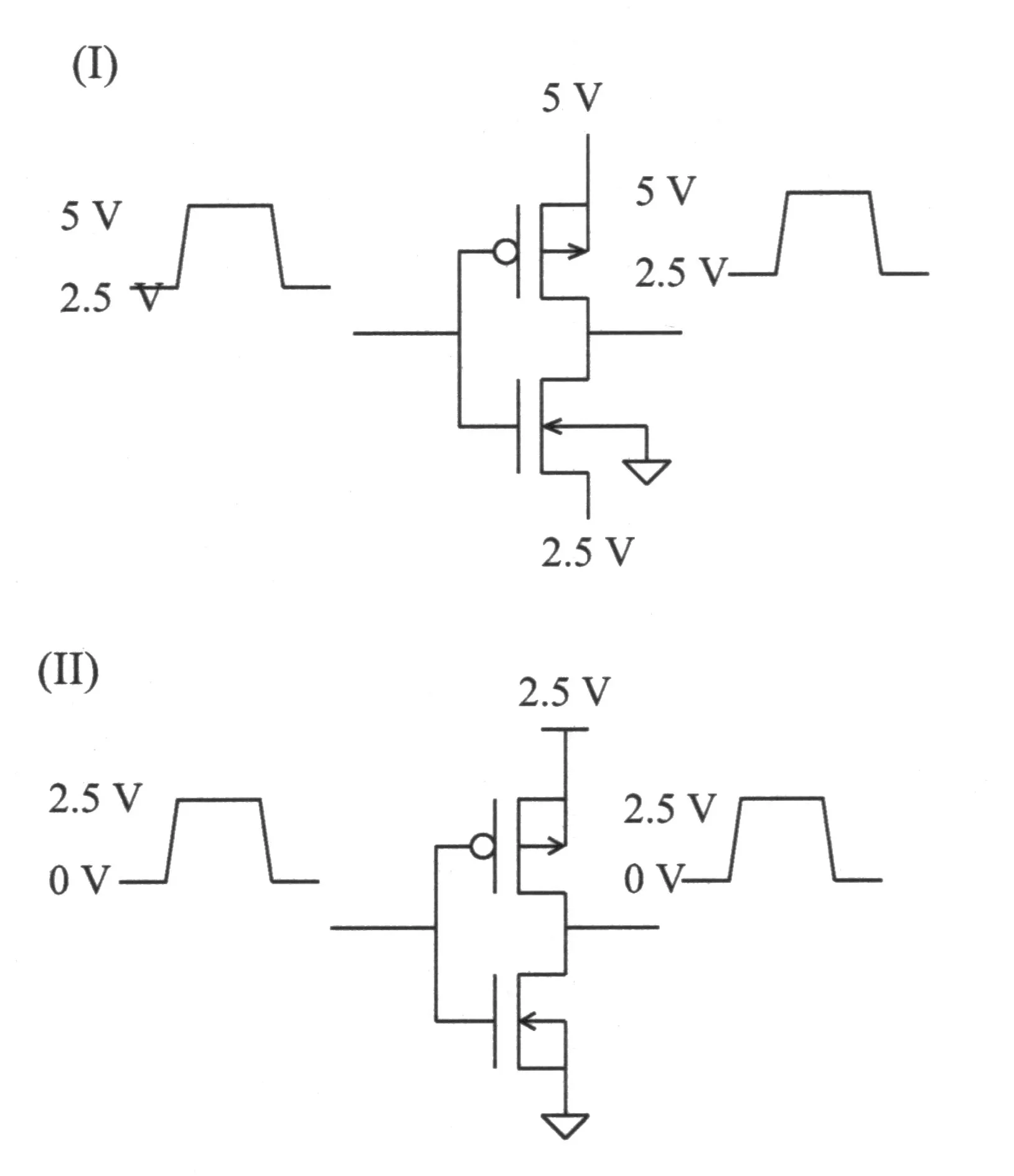
FN10-1, p2 (Fall 2010, 10 points). Joe Engineer decides he wants to design logic circuits that operate between 2.5 V and 5 V (rather than between 0 V and 2.5 V). Consider an inverter in this circuit style shown in (I). How will the rising and falling delays of this inverter compare with the “regular” logic scheme of (II) for the same output loading and input slew times?
Hint
What it asks. How the rising and falling delays of the shifted inverter (I) compare with those of the ordinary one (II). “For the same output loading and input slew times” removes every other difference: only the transistors’ bias can change the delays.
The idea. This is the threshold section’s term (How to approach). A transistor responds to the voltages between its own terminals, not to their values above ground. Shifting a whole circuit up by 2.5 V changes nothing, unless some terminal isn’t shifted. Here one is: the NFET’s body stays at ground. A source above its body is a reverse bias , which deepens the depletion region under the gate. Then grows, and so does (Chapter 5, Section 1). A higher threshold at the same leaves less overdrive, and less current. The delay is charge over current (Chapter 5, Section 11), so the edge that device drives gets slower.
Rising and falling edges
- Measure from each source. Because a transistor feels only the voltages between its own terminals, look at each one relative to its source. Both circuits swing 2.5 V, so every gate-to-source voltage is the same in (I) and (II): 2.5 V when on.
- Rising output (the PFET pulls up). Because the PFET drives this edge, compare its terminals: in (I) its source is at 5 V and its body (the n well) at 5 V, the same relation as in (II). Same , same threshold, same current: the rising delay is about the same.
- Falling output (the NFET pulls down). Because the NFET drives this edge, compare its terminals: in (I) its source is at 2.5 V but its body is drawn to ground: . The depletion region under the gate must hold , so and rise (Chapter 5, Section 1).
- Less current, a slower edge. Because the NFET has the same and a higher , its overdrive is smaller, its current lower, and the falling delay longer.
- How much, in Chapter 5’s device added (). At the bulk charge doubles and . The overdrive falls from 2.0 to 1.74 V. A velocity-saturated current falls in proportion, so the falling delay grows by (15%); a square-law current would make it 1.32 (32%).
Check. Remove the cause. Tie the NFET’s body to its own source at 2.5 V instead of ground: then , every terminal of both devices is shifted by the same 2.5 V, and (I) behaves exactly like (II) on both edges. Only the body tie changed, so the body tie causes the slower fall.
Answer: the rising delay is about the same (the PFET sees the same overdrive and the same body bias); the falling delay is longer in (I), because its NFET’s body is 2.5 V below its source, and the body effect raises its threshold and cuts its overdrive.
A smaller effect the other way added. The NFET’s drain junction in (I) is reverse-biased by 2.5 to 5 V instead of 0 to 2.5 V, so its junction capacitance is smaller (Chapter 5, Section 5): in Chapter 5’s junction, 0.486 down to 0.371 fF/µm² instead of 0.905 down to 0.486. That speeds both edges a little; it does not undo the body effect on the falling edge. The question does not need it.
Remember. Never compare absolute voltages: read each device’s and from its own source. A body below an NFET’s source raises its and slows the edge that NFET drives.
The answer key agrees
It gives the same: rising about the same, falling slower because the NFET is body affected (). It does not mention the smaller drain-capacitance effect in the other direction.
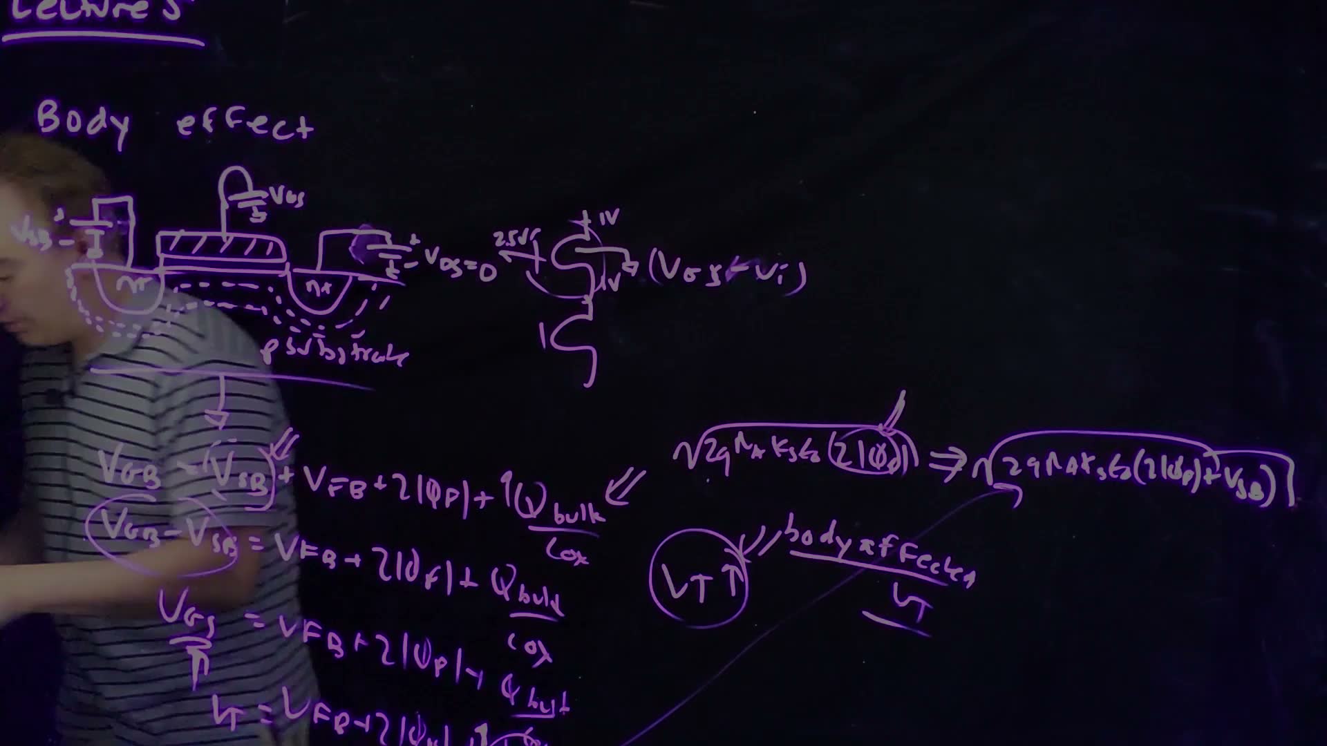
Set to 2.5 V to see the falling edge’s threshold in (I):
4. Delay as charge over current: FO1, FO4 and the supply
FN12-2: why FO1 is more than a quarter of FO4
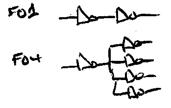
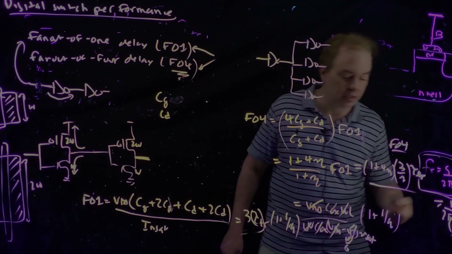
FN12-2, p5 (Fall 2012, 6 points). In general one finds that the fanout-of-one (FO1) delay is greater than one-fourth the fanout-of-four (FO4) delay. Why is this?
Hint
What it asks. Why FO1 is more than a quarter of FO4: why four loads don’t take four times as long. “Why” asks for the reason, a count of the capacitance on the output node.
The idea. This is the charge-over-current move of M3’s device short answers, and the same counting as MT21-2. What this question adds is that it asks for the reason instead of the formula, with the lecture’s 2W/W inverter. The output node at holds the charge , and the switching transistor, saturated, removes it at , so (Chapter 5, Section 11). The driver is the same in both cases, so the current is too, and the delay is in proportion to the capacitance on the node. The tempting answer, FO4 = 4 × FO1, counts four drivers’ drains where there is one.
- Charge over current. A delay is the charge to move over the current: (Chapter 5, Section 11). Because the driver, and so the current, is the same in both cases, only the capacitance differs.
- Count the node. Because the node is the driver’s output, it carries the loads’ gates and the driver’s own drains. FO1’s node carries one load’s gate capacitance and the driver’s drain capacitance: . FO4’s carries four loads’ gates but still one driver’s drain: (Chapter 5, Section 13).
- Divide. Because the current is the same, the two delays are in the ratio of their node capacitances: with , which is less than whenever .
- For scale, at η = 2. The lecture’s inverter is 2W/W, and its FO1 is , where is the transit time and the 3 counts the 2W PFET’s capacitance (Chapter 5, Section 12). So and , so and is of it. With : 11.25 ps against 8.44 ps.
Check. The limits of the ratio . With no drain capacitance () it is 4, and FO1 is exactly a quarter of FO4. With more drain capacitance it falls: 3 at , 2.5 at . The more of the node the driver’s own drains make up, the less the fanout matters.
Answer: the driver’s own drain capacitance is in both loads, but it does not grow with the fan-out. FO4 has four times the gate load and the same drain load, so a quarter of FO4 carries only a quarter of the drain capacitance, while FO1 carries all of it. Only with no drain capacitance () would FO1 equal FO4/4.
Remember. Count the loads’ gates times the fanout, and the driver’s drains once. In Chapter 7’s RC model, which ignores drain capacitance, FO4 is exactly (M2, Section 2 explains the two models).
The answer key agrees
FN10-6a: supply sensitivity of a velocity-saturated inverter
FN10-6, p9 (Fall 2010). One of the issues in using inverters as delay elements (or in distributing clocks) is that they have a high sensitivity to power-supply variations. Let’s try to calculate this (back-of-the-envelope).
(a) (10 points) To estimate the delay, assume that the inverter is driven by a step input, the discharging (or charging) transistor is always saturated (with full overdrive), and the device is completely velocity saturated. Variations in the supply voltage affect both the logic high level of the inverter input as well as the supply of the inverter. If and , find the power supply sensitivity .
Hint
What it asks. By what percentage the delay changes when the supply changes by 1%: that is what measures. “Affect both the logic high level of the inverter input as well as the supply” says that appears twice: in the charge on the node and in the overdrive. “Completely velocity saturated” picks the current law.
The idea. The delay is charge over current, the move of M3’s device short answers: the node holds , and the step input gives the switching transistor the full overdrive . A fully velocity-saturated current is in proportion to the overdrive, (Chapter 4, Section 7). What this question adds is the logarithmic derivative added: , the fractional change in per fractional change in . Taking the logarithm turns the delay’s product and quotient into a sum and a difference, so each factor contributes on its own. In words: the charge grows in proportion to , which lengthens the delay, while the current grows in proportion to the overdrive, which shortens it. The overdrive changes by a larger fraction than , because doesn’t move.
Velocity-saturated
-
Charge over current (Chapter 5, Section 11): . Because the step input reaches , the overdrive is .
-
The current law. Because the device is fully velocity-saturated (Chapter 4, Section 7), . So .
-
Take logarithms added, because the sensitivity is the derivative of with respect to : , so
-
The numbers. , : .
-
Read it. A 1% lower supply makes the delay 0.25% longer. The charge to move falls with , and the current falls slightly faster, by .
Check. Compute two delays directly. At 2.5 V, ; at 1% more supply, 2.525 V, . That is 0.25% shorter for 1% more supply: a sensitivity of −0.25. ✓
Answer: .
Remember. Supply sensitivity is the exponent of in the charge (1) minus the current’s exponent of the overdrive times . The current feels the overdrive, not the supply, so the threshold is what makes a delay supply-sensitive.
The answer key agrees
FN10-6b: the same with a square-law device
FN10-6b, p9 (10 points). If the device were “square-law” (i. e., not velocity saturated), what would the power-supply sensitivity be?
Hint
What it asks. The same sensitivity as (a), for a device whose saturated current follows the square law instead.
The idea. Everything in (a) stays except the current law. The long-channel saturated current goes as the square of the overdrive, ; it holds when the carriers are not velocity saturated (Chapter 4, Section 4). In the logarithm the square becomes a factor 2, so the current’s term in (a)‘s sensitivity counts twice added.
Square law
-
The current law. Because the device is square-law (Chapter 4, Section 4), , so .
-
Take logarithms, as in (a), because the sensitivity is : , so
-
The numbers. .
-
Compare with (a). It is six times the velocity-saturated value, because the current now falls as the square of the overdrive.
Check. Compute two delays directly again. At 2.5 V, ; at 2.525 V, . That is 1.5% shorter for 1% more supply. ✓
Answer: .
Why velocity saturation helps here added. With a velocity-saturated delay doesn’t depend on the supply at all (), while a square-law delay still goes as , sensitivity . The sensitivity is a slope: for a large droop, compute the two delays directly. From 2.5 V to 2.0 V (20% lower) the velocity-saturated delay grows by 6.7% (the slope alone says 5%) and the square-law delay by 42% (the slope says 30%).
Remember. The current’s exponent of the overdrive multiplies its share of the sensitivity: 1 for velocity saturation, 2 for the square law. A velocity-saturated device is much less sensitive to its supply.
The answer key agrees
Its last line, which the transcription reads as “−0.25)6”, is , that is .
What to notice.
- At the exam’s values the two readouts are −0.25 and −1.50.
- Raise toward : both sensitivities grow without bound, because the overdrive is what the supply really moves.
- Chapter 4’s full velocity-saturation model lies between the two curves, closer to the linear one for short channels (compare H1’s doubling test).
Check yourself A velocity-saturated inverter runs at VDD = 1.0 V with VT = 0.3 V. What is its supply sensitivity, and why is it larger than FN10-6a's?
. The threshold is a larger fraction of the supply, so a given change in moves the overdrive by a larger fraction. Low-voltage designs are more supply-sensitive.
Formulas this page uses
- Threshold (the approach): , , (Chapter 3, Section 8; Chapter 5, Section 1). Less bulk charge for the gate (DIBL, roll-off) or a thinner oxide: lower . More doping (halos) or : higher .
- Subthreshold: ; a current-defined is (Chapter 4, Sections 8 and 11).
- FO1 and FO4: , (Chapter 5, Sections 12–13).
- Supply sensitivity of : ; velocity-saturated (), square law ().
What this means for the midterm
Device short answers (MT17-1b–c, MT21-2; M3, Sections 8–9).
- Counting decades (FN12-1a–b) is the move of MT17-1c, of the leakage step in MT24-2b and MT23-1b, and of HW1-3. Trap: is gate to source; a raised source counts. About 2 minutes.
- Body connections (FN10-1) are MT17-1b’s question from the other side: a body below an NFET’s source is a reverse bias that raises ; a body on the wrong side of a junction forward-biases it. Trap: comparing absolute voltages instead of each device’s and . About 3 minutes.
- FO1 and FO4 (FN12-2) is MT21-2: count the gates of the loads and the drains of the driver only. Trap: FO4 = 4 FO1. About 3 minutes.
Explanation questions (FN19-2, FN17-1a, 1c, FN12-1c). The midterms ask few of these, but the instructions give partial credit for explanations. Answer from the threshold formula, with the approach’s four moves. Two or three sentences each.
Not asked by any past midterm. The supply sensitivity (FN10-6) and the short-channel effects (FN19-2, FN17-1a) appear only in the finals. They test the same two I–V models as M2’s chart.
What the keys get wrong
The 2019 final has no key. Every other part agrees with its key after re-solving; these notes are recorded in this page’s review/decisions.md.
| Part | The key | Here |
|---|---|---|
| FN17-1c | thinner oxide, lower , because “the gate has full control of the bulk charge” | direction right; the reason is the oxide term , which shrinks with while stays |
| FN12-1c | (i), because node A rises and cuts the top device’s leakage | (i) is right; the raised node alone (part b’s assumptions) is not enough: the body effect and the bottom device’s missing DIBL carry the difference |
| FN10-1 | rising the same, falling slower (body effect) | agrees; it leaves out the smaller drain-capacitance effect in the other direction |
FN17-1a, FN12-1a–b, FN12-2 and FN10-6a–b agree with their keys.