FS1. Final practice: flip-flop and latch timing
This page practises the timing questions of the final’s sequential part: two flip-flops whose clocks arrive at different times, a pair of local clock generators, clock jitter from a noisy supply, and loops of transparent latches. Every past-final part on these topics and Problem Set 5’s latch question are here, re-solved from the papers’ figures; the keys’ numbers are not copied. They come in two families. Flip-flop timing (FN17-5, FN12-7b, FN10-6c–d) is about one pair of clocked elements: does the data arrive early enough for the next edge (setup, the long path) and late enough not to spoil this one (hold, the short path)? Latch loops (PS5-Q1a–e) walk data through transparent latches edge by edge, around a loop. Each family opens with a How to approach section that gives the model and the moves once, and ends with harder added variations: longer chains, setups no past paper uses, and heavier arithmetic, as the real Fall 2026 midterm was.
Every part is worked the same way: what it asks, the idea, why this formula, the solution in steps (each gives its reason first), a check by another route, the answer, and what to remember. Try each part first; open the Hint if you are stuck. The answer key’s verdict is folded at the end of each past-paper part.
Before you start. Everything here is taught in Chapter 13 and Chapter 14, and each section below restates what it uses:
- a flip-flop made of two latches, and which edge is active (Chapter 13 §10: the master’s closing edge captures, the slave’s opening edge launches);
- the long path (Chapter 13 §11, Chapter 14 §1) and the short path (Chapter 14 §2);
- the non-overlap window and the local generator (Chapter 14 §3);
- the two rules of the road and the latch walk (Chapter 14 §8, §9).
Conventions on this page. Every latch is transparent high: open while its clock is 1, closing on the falling edge. Skew is written with a sign, as Chapter 14 does added: = (the capturing element’s clock edge) − (the launching element’s clock edge), so is a late capture clock. Times are in the paper’s unit.
Symbols
| Symbol | Meaning | Unit | First appears |
|---|---|---|---|
| φ1, φ2 | the two phases of a two-phase clock (complementary unless a question says otherwise) | — | FN17-5 |
| φ1′, φ2′ | the same phases at a second, skewed pair of latches | — | FN17-5 |
| the clock period (the papers’ “cycle time”) | ps, ns | FN17-5 | |
| clock-to-Q delay: from the edge that opens a latch (the slave, in a flip-flop) until Q changes; the papers write | ps | FN17-5 | |
| D-to-Q delay of an open latch; the papers write | ps | FN17-5 | |
| , | how long before and after a latch’s closing edge D must be steady | ps | FN17-5 |
| the delay of the combinational logic between two clocked elements | ps, ns | FN17-5 | |
| the size of the skew between two clocks | ps, ns | FN17-5 | |
| signed skew: capture edge minus launch edge, positive when the capture clock is late added | ps, ns | approach A | |
| the length of the non-overlap window, when both phases are low (Chapter 14’s board name) | ps, ns | approach A | |
| φ, φ̄ | the global clock a local generator starts from, and its complement | — | FN12-7 |
| CLK1, CLK2 | the global clock at two different generators | — | FN12-7 |
| , | the delay blocks of FN12-7’s generator | ns | FN12-7 |
| supply sensitivity of a delay, | — | FN10-6 | |
| , | supply and threshold voltage | V | FN10-6 |
| L1 … L4 | the latches of a loop, in the order the data visits them | — | approach B |
How to approach a flip-flop timing question
Recognize it by the picture: two clocked elements with logic between them, and something wrong with their clocks. The finals draw each flip-flop as its two latches, so four latches in a row on φ1, φ2, φ1′, φ2′ are two flip-flops, and a clock generator box (CG) per pair means each pair’s clocks are made locally. The prompts are: “will this circuit function correctly”, “what is the largest value of ”, “how must and be adjusted”, and “could this jitter cause a failure that slowing the clock cannot fix”.
The model. A flip-flop built from a master latch and a slave latch captures when the master closes and launches when the slave opens (Chapter 13 §10). Its setup and hold times are the master’s; its is the slave’s. The latches’ never enters a flip-flop-to-flip-flop check: inside the pair the slave is closed whenever the master’s output moves. Between two flip-flops, two things must be true.
- The long path (setup, late mode). The data launched at one edge must reach the capturing flip-flop before its next capture edge. That edge comes one period after the launch, moved by the skew, so .
- The short path (hold, early mode). The same data must not reach the capturing flip-flop before the capture edge of the same cycle plus , because that edge is still storing the previous cycle’s data: .
Why these two, and their conditions. Draw the launch edge at . The new data leaves the launching flip-flop at and arrives at . The capturing flip-flop’s edge of the same cycle is at , and its next edge at . Setup needs the arrival before the next one; hold needs it after this one. The board writes both with a magnitude and picks the sign per case (Chapter 14 §1–§2); the signed form does it once. Both are Derive: three lines from that picture. They assume one value per delay (the course does not separate minimum and maximum delays) and edge-triggered behaviour, which the latch pair gives only if its two clocks do not overlap.
The moves.
- Read the pairs. Which latch is the master (the first one the data meets)? Its closing edge is the capture edge; the slave’s opening edge is the launch.
- Set the sign. Write for the pair from the words: “arrive 50 ps earlier” at the capturing pair is ps; “CLK2 arrives 1.5 ns later” at the capturer is ns.
- Check hold first. It does not contain , so a failure there is a “chip killer”: no clock frequency fixes it.
- Then the long path. A failure there only slows the chip.
- Repairs. A hold failure is fixed by padding the short path (buffers) or, if the latch clocks are made locally, by a non-overlap window between the master’s closing and the slave’s opening, ; the window is dead time, so every stage’s long path loses it (Chapter 14 §3).
- Jitter is an edge that moves transiently (Chapter 23’s topic, taught in place under FN10-6). For each check, put it where it hurts: as a late capture edge for hold, an early one for setup.
Decide on the way: the sign of ; which phase drives the master; which of a generator’s two delays sits between the master’s closing and the slave’s opening.
Traps. Treating four latches as four stages. Taking from the master, or adding . Comparing hold with the next edge (that is setup). Thinking a slower clock fixes hold. Forgetting that time a late capture clock gives one stage is taken from the next: that stage launches from the late clock and gets .
FN17-5: four latches, two flip-flops, 50 ps of skew (40 points)
You need
A flip-flop from two latches (Chapter 13 §10). A transparent-high latch passes D to Q while its clock is high and holds when the clock falls. A latch on φ1 followed by a latch on φ2, the complement of φ1, is a master–slave flip-flop: the master (φ1) closes at φ1’s falling edge and keeps D, and at that same instant the slave (φ2) opens and shows it. So the pair captures and launches at φ1’s falling edge. Setup and hold belong to the master, to the slave; the latches’ plays no part between two such pairs.
The long path with skew (Chapter 14 §1). Data launched at one edge must arrive before the capturing flip-flop’s next edge, one period later and shifted by the skew: , where is the capture edge minus the launch edge. An early capture clock () shortens the budget.
The short path (Chapter 14 §2). The same data must not arrive before the capture edge of the same cycle plus : . A late capture clock () is what makes this bite; an early one helps.
The question (FN17-5, p11, in the paper’s words). Consider the path through the two flip-flops shown below. Assume that the and clocks are skewed to arrive 50 psec earlier than the corresponding and clocks. Let each latch be characterized by psec, psec, and psec. Let the cycle time of the clock be 500 psec.
FN17-5’s path (p11, redrawn). Left to right: a latch on φ1, a latch on φ2, the logic , a latch on φ1′, a latch on φ2′. Read in pairs, it is two master–slave flip-flops with the logic between them.
The exam’s own figure (FN17-5, p11)
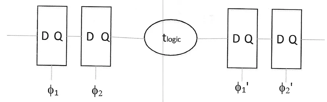
Reading the figure. The paper calls it “two flip-flops”, so read the latches in pairs: (φ1, φ2) is the launching flip-flop and (φ1′, φ2′) the capturing one. The paper does not draw the clocks. Take φ2 as the complement of φ1, as a two-phase clock from one wire is (the key’s own sketch draws them so), and φ1′, φ2′ as the same waveforms shifted 50 ps earlier. Put φ1’s rising edge at : φ1 is high on [0, 250) ps of each 500 ps cycle and φ2 on [250, 500). The first flip-flop launches when its slave opens, at 250 ps. The second captures when its master, the φ1′ latch, closes: φ1′‘s falling edge, at 200 ps in the same cycle and 700 ps in the next. No hold time is given; take .
Part (a): does it work with no logic? (10 points)
FN17-5a, p11. If psec, will this circuit function correctly? Explain. (10 points)
Hint
What it asks. Whether the pair works when the two flip-flops are wired straight to each other, the shift-register case. Of the two checks, the long path has all the time it wants here (), so the question is really about the short path: can the new data arrive so early that the capturing flip-flop takes it in the wrong cycle? The word that decides the method is “earlier”: it fixes the sign of the skew.
The idea. The short path compares the earliest arrival of the new data with the capture edge of the same cycle plus the hold time. A capture clock that arrives early closes the receiving master before the launching slave even opens, so the new data cannot catch it. Early skew is harmless to hold; it only costs the long path, which part (b) asks about.
Why this formula. The short-path condition is .
- Where it comes from. At the launch edge ( in the pair’s own frame) the slave opens and Q changes later; the logic passes the change on after . The receiving master closes at on the previous cycle’s data, and D must stay still until . The new data must not come before that.
- Why it applies. The pairs are flip-flops, and the receiving pair’s setup and hold are its master’s; is the launching slave’s, 10 ps. The paper gives no hold time, so .
- The sign. The primed clocks are 50 ps earlier, so the receiving master closes 50 ps before the launching slave opens: ps.
- The tempting alternative. Using as if skew always hurt hold. That is the late case, and Variation 1 shows it fails there. And does not enter: data does not flow through an open slave here; the slave opens on a master that has already closed.
FN17-5 as printed, computed from its values added: the primed clocks lead φ1 and φ2 by 50 ps. Data launched as φ2 opens at 250 ps first changes after ps, at 260 ps; φ1′ had already closed at 200 ps, 60 ps before. The bar from 250 to 700 ps is the long path’s budget up to φ1′‘s next falling edge, which part (b) works out.
FN17-5a
- The launch. Because the first pair launches when its slave opens, the new data leaves at φ2’s rising edge, 250 ps, and appears at the slave’s Q at ps.
- The capture edge it must not beat. Because the receiving pair captures when its master closes, the edge that is storing the old data is φ1′‘s falling edge of the same cycle: ps.
- Compare. With no logic the new data reaches the receiving master at 260 ps, and that master closed at 200 ps.
- In the formula. ps against ps: , with 60 ps to spare. The bound on the logic is ps: no constraint at all.
- The long path at . The data must reach the receiving master before φ1′‘s next falling edge, 700 ps, minus 5 ps of setup. It arrives at 260 ps: fine.
Check. Count in the latches’ own terms. The danger in a two-phase pair is a moment when the launching slave (φ2) and the receiving master (φ1′) are both open, because then new data can run from one to the other in the same cycle. φ2 is high on [250, 500) ps; φ1′, 50 ps early, is high on [−50, 200) and [450, 700). They overlap on [450, 500), but by then the first master (φ1) has been closed since 250 ps, so the data passing through is the very data φ1′ is meant to capture at 700 ps: no harm. The window that would matter, φ2 opening while φ1′ still holds the previous data, does not exist, because φ1′ shut at 200 ps.
Answer: yes. The early capture clock closes the receiving master 50 ps before the new data is launched, so there is no early-mode (hold) problem, with 60 ps of margin; the long path at is easily met.
Remember. Early capture clock: hold is safe, the long path pays. Late capture clock: the reverse. Check hold first with the sign written down.
The answer key agrees
Part (b): the largest logic delay (10 points)
FN17-5b, p11. What is the largest value of for which the circuit will work? Explain. (10 points)
Hint
What it asks. The longest logic that still lets the data reach the second flip-flop in time for the next capture edge. “Largest” says it is the long path (setup, late mode). The unknown is ; everything else is given.
The idea. The data has from the launch to the next capture edge, minus what the flip-flops themselves use: the slave’s at the start and the master’s at the end. The capture clock being early moves that next edge 50 ps closer, so the logic loses 50 ps.
Why this formula. .
- Where it comes from. The launch is at 0; the receiving master’s next closing edge is one period later, shifted by the skew, at . The data must be steady before it, and it starts moving only after the launch.
- Conditions. Edge-triggered flip-flops (the pairs, with complementary clocks), one period between launch and capture, one delay per block. It is checked at the slow corner.
- Which delays. = 10 ps (the launching slave), = 5 ps (the receiving master). The = 10 ps is not used: in a flip-flop-to-flip-flop path the data never passes through an open latch. If it arrives while the receiving master is open, it waits there until that master closes; the receiving slave is shut meanwhile.
- The tempting alternatives. Adding (a 425 ps answer). Using for the early clock (535 ps): an early capture edge comes sooner, so it can only take time away.
FN17-5b
- The edges. Because the receiving pair captures when φ1′ falls, and φ1′ is 50 ps early, the next capture after the 250 ps launch is at ps; the data must be steady at the master’s D by ps.
- The start. Because the new data appears only when the launching slave has opened and switched, it starts through the logic at ps.
- The budget. Because the logic must fit between those two times, ps.
- The same in the formula. ps. With no skew it would be 485 ps; the early clock costs exactly its 50 ps.
Check. Count the skew across both stages. The stage after the primed pair launches from the early φ1′, φ2′ into the next on-time pair, so its capture edge is 50 ps late relative to its launch: ps. The two stages together get ps, exactly what two unskewed stages get. Skew moves 50 ps from this stage to the next and creates no time, which confirms the sign of the 50 ps as well as its size. Part (a)‘s hold check sets no lower bound (−60 ps), so the working range is ps.
Answer: ps. The of 10 ps does not enter.
Remember. Long path = period + signed skew − − . When a paper gives as well, ask whether the data ever passes through an open latch; between two flip-flops it does not.
The answer key agrees
Part (c): repairing the clocks (10 points)
FN17-5c, p12. If the circuit is not functional in (a), how can the and clocks be modified such that the circuit will function correctly. (10 points)
Hint
What it asks. A repair for a hold failure in (a), made by changing the unprimed clocks. The words “if … not functional” make the part conditional on (a)‘s answer.
The idea. Part (a) found the circuit functional: the early capture clock closes the receiving master 50 ps before the launch, and the hold margin is 60 ps. With the condition false there is nothing to repair. The repair the question has in mind belongs to the other sign of skew, a late capture clock; Variation 1 solves the paper with that reading.
Why this formula. The test of the condition is part (a)‘s short path, : the new data leaves after the launch and must not reach the receiving master until after its closing edge of the same cycle. With ps the right side is negative, so even passes. A repair would act on this inequality: a non-overlap window between the launching master’s closing and its slave’s opening, made by pulling φ1’s falling edge earlier or by delaying φ2’s rising edge, delays the launch relative to the hold-critical capture and adds to the left side (Chapter 14 §3). Neither is needed when the inequality already holds. The tempting move is to “fix” the 50 ps anyway by delaying the primed clocks: that removes the skew, but the paper says the circuit works, and changing φ1′ is not what it asks.
FN17-5c
- Test the condition. Because the part applies only if (a) failed, recall (a): , true with 60 ps to spare.
- Conclude. Because the condition is false, no modification of φ1 and φ2 is required.
- Say what you would do if it were true (a sentence earns its keep on an exam). A hold failure from a late capture clock is repaired by a non-overlap window between φ1’s falling and φ2’s rising edge, at least wide, made by pulling φ1’s falling edge earlier or by delaying φ2’s rising edge; either way it costs the long path that much.
Check. The latch picture of (a) agrees: φ1′ closes at 200 ps and φ2 opens at 250 ps. There is already a 50 ps gap between the receiving master’s closing and the launching slave’s opening, exactly what a repair would have to create.
Answer: the circuit in (a) works, so no change to φ1 and φ2 is needed.
Remember. Read conditional parts literally. If the sign of the skew makes the part moot, say so in one line and state the repair for the other sign.
The answer key agrees
Part (d): the largest logic delay now (10 points)
FN17-5d, p12. What is the largest value of now for which the circuit will work? Explain. (10 points)
Hint
What it asks. The long-path limit after the repair of (c). The word “now” ties it to (c).
The idea. Part (c) changed nothing, so the clocks are those of (b) and so is the answer. Had (c) opened a non-overlap window , the launch would move that much later relative to the capture and the limit would fall by .
Why this formula. The same long path as (b): . It comes from the launch at the slave’s opening and the deadline before the receiving master’s next closing; a window delays the slave’s opening relative to that closing by (Chapter 14 §3, the dead time). With no window, and the formula is (b)‘s. The conditions are (b)‘s: flip-flops, one period, the slow corner; again plays no part.
FN17-5d
- What changed. Because (c) required no modification, and ps as before.
- The limit. Because the long path is unchanged, ps, as in (b).
Check. The working range is still ps: the short-path bound of (a), −60 ps, imposes nothing, and the long-path bound is (b)‘s. A window would only have narrowed it from above.
Answer: 435 ps, the same as (b).
Remember. A repair that delays the launch is paid for in the long path, one for one. No repair, no cost.
The answer key agrees
FN12-7b: two clock generators, 1.5 ns apart (15 points)
You need
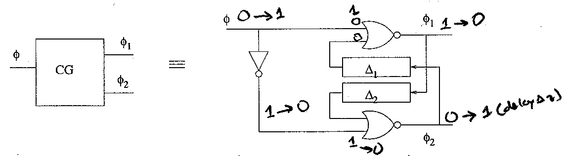
A NOR’s output is high only when both inputs are low. That one fact runs FN12-7’s generator: and , where is φ2 delayed by (Chapter 14 §3 works it through; gate delays ignored).
- When φ rises, φ1 falls at once (φ is one of its NOR’s inputs), and φ2 rises only later, when the delayed φ1 has gone low.
- When φ falls, φ2 falls at once ( goes high), and φ1 rises only later.
So φ2 is high roughly while φ is high and φ1 while φ is low, and each delay opens a window in which both phases are low: after φ1 falls, after φ2 falls.
The flip-flop and its edges (Chapter 13 §10). In a pair of latches the first one the data meets is the master. The pair captures when the master closes and launches when the slave opens; if the two phases have a gap between them, the launch comes that gap after the capture.
The short path (Chapter 14 §2–§3). The new data must not reach the capturing flip-flop before its capture edge of the same cycle plus : with the capture clock late by and the launch delayed by a window , . No appears.
The question (FN12-7, p8–p9, in the paper’s words). Consider the “local clock generator” circuit shown below, used to generate two clock phases locally from a single-wire global clock. The delay blocks (labelled with and ) could be implemented with an even number of inverters (for example).
FN12-7’s local clock generator (p8, redrawn; the key’s handwritten logic levels are left out). The box CG stands for the circuit: φ drives the top NOR, whose output is φ1; drives the bottom NOR, whose output is φ2; φ2 is fed back through to the top NOR and φ1 through to the bottom one.
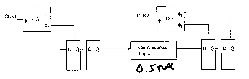
(b) Consider two latches driven by two different clock generators as shown below: Let CLK1 and CLK2 each have 10nsec periods, but let there be skew between CLK1 and CLK2 such that CLK2 arrives 1.5nsec later than CLK1. Ignoring latch overhead and skew introduced by the clock generators and assuming that the combinational logic represented a fixed delay of 0.5nsec, how must and in the clock generators be adjusted (from zero) to ensure correct functionality? Please assume that both clock generators must be adjusted in the same way and carefully explain your answer. (15 points)
On the paper, “latches” is crossed out by hand and replaced by “flip-flops”: each latch pair is one flip-flop.
FN12-7b’s system (p9, redrawn). Each flip-flop is two latches clocked by its own generator: the first latch of each pair on φ2, the second on φ1. Between the pairs, 0.5 ns of logic (the paper labels the block “Combinational Logic”; 0.5 ns is the statement’s value).
The exam’s own figures (FN12-7, p8 and p9)
Part (b): adjusting Δ1 and Δ2 (15 points)
Hint
What it asks. CLK2 reaches the second generator 1.5 ns after CLK1 reaches the first, and only 0.5 ns of logic separates the flip-flops. The question asks which generator delay to raise from zero, and by how much, so that the circuit works. “From zero” says that, as drawn, it does not. “Ignoring latch overhead” sets , and to zero. “Both generators the same” means one setting serves both.
The idea. A late capture clock with a short path is Chapter 14’s hold failure: the new data reaches the receiving master while that master is still open on the old data. The cure that needs no change to the logic is to launch later, by opening a gap between the launching flip-flop’s master closing and its slave opening. The generator has two delays, and only one of them sits in that gap. Which one depends on the phase the master is on, so read FN12-7b’s flip-flop figure first.
Why this formula. The condition is the short path with a window, , here with every overhead zero: .
- Where it comes from. Put CLK1’s falling edge at 0. The launching master (φ2 of CG1) closes there. If the slave (φ1 of CG1) opens later, the new data leaves at and reaches the receiving master at . The receiving master (φ2 of CG2) closes on the old data at CLK2’s falling edge, ns. The new data must not get there sooner.
- Which delay is the window. In this generator φ2 falls at once when φ falls, and φ1 rises later. With the master on φ2 and the slave on φ1, the gap from the master’s closing to the slave’s opening is exactly . is the other gap, from φ1 falling (the slave closing) to φ2 rising (the master opening): it moves neither the launch nor the capture.
- Conditions. Gate delays and latch overhead ignored (the paper says so), the generators’ own skew ignored, a fixed logic delay (so the shortest and longest paths are both 0.5 ns), and each delay shorter than the half period it sits in, or the generator’s phase never rises.
- The tempting alternative. Taking Chapter 14’s board flip-flop (master on φ1), whose window is . On this paper the master is on φ2, so that answer is wrong.
FN12-7b
- Read the generator. Because a NOR is high only when both inputs are low, φ falling drops φ2 at once and lets φ1 rise later; φ rising drops φ1 at once and lets φ2 rise later.
- Read the flip-flops. On p9 the first latch of each pair is clocked by φ2 and the second by φ1. So each master is on φ2: it captures when φ2 falls, at the falling edge of its global clock. Each slave is on φ1: it launches when φ1 rises, after that falling edge.
- The two edges that race. Because the first flip-flop launches when its slave opens, the launch is at CLK1’s falling edge plus . Because the second captures when its master closes, the old data is held until CLK2’s falling edge, 1.5 ns after CLK1’s.
- As drawn (). With CLK1 falling at 5 ns, the new data leaves at 5 ns and arrives at 5.5 ns, while the receiving master stays open until 6.5 ns. It arrives 1.0 ns too soon: the new data enters CG2’s master in the same cycle and overwrites the value that master should still hold.
- The condition. Because the window delays the launch, , so ns. With ns, the slave opens at 6 ns and the data arrives at 6.5 ns, exactly as the receiving master closes.
- . Because only delays the master’s opening, it does not help hold. It costs nothing here either, but it shortens the master’s window for no gain: leave .
- The other limits. Because the window is dead time, the long path loses : the data launched at ns must reach the receiving master before its next closing edge, CLK2’s falling edge at ns, so , that is ns, which never binds. The generator sets the real ceiling: must stay below the half period, 5 ns, or φ1 would not rise before φ rises again.
- Both generators the same. CG2 gets the same . That moves only its own slave, which launches into whatever comes after; its capture edge (CLK2 falling) does not move.
FN12-7b computed from its values added. (a) With , CG1’s slave (φ1) opens as CLK1 falls at 5 ns, and after 0.5 ns of logic the new data reaches CG2’s master (φ2) at 5.5 ns, while that master stays open until CLK2 falls at 6.5 ns: a race. (b) With ns the slave opens at 6 ns and the data arrives at 6.5 ns, just as the master closes; the next capture is at 16.5 ns.
Check. Two other routes. First, try the delay the question tempts you to raise. With ns and , each generator’s φ2 rises 1 ns later, so CG2’s master opens at 2.5 ns instead of 1.5 ns; but it still closes at 6.5 ns, when CLK2 falls, and the data still leaves at 5 ns and arrives at 5.5 ns. The race is unchanged, 1.0 ns short: is not the knob. Second, size the repair the other textbook way, by padding the logic. The data must not arrive before 6.5 ns, so the 0.5 ns path would need ns more delay. Delaying the launch by and delaying the arrival by padding must cost the same, and they do: 1.0 ns.
Answer: raise to at least 1.0 ns in both generators (and below 5 ns, the half period); leave . The window between each master’s closing (φ2 falling) and its slave’s opening (φ1 rising) then delays the launch enough that the 0.5 ns path no longer beats CLK2’s 1.5 ns late capture.
Remember. The window that cures hold is the one from the master’s closing to the slave’s opening. Find which phase the master is on before you pick or .
The answer key agrees
FN10-6c–d: jitter from a noisy supply (15 points)
You need
Skew and jitter (Lecture 22, the board at 18:32–20:41; Chapter 23 will teach it, and it is restated here). The clock is driven from one point and should reach every flip-flop at the same instant. Skew is a static difference in arrival time: a fixed offset, for example from process variation across the die. Jitter is a transient difference in arrival time: the edge “can move around”, and “can change from cycle to cycle”, so “one cycle can be shorter, another cycle can be longer”. Its usual source is supply noise: “power supply noise that causes the buffer delay here to be different from the buffer delay over here transiently”. The clock tree’s latency, its root-to-leaf delay, is what turns such variation into skew and jitter: the more delay there is, the more a given percentage change moves the edge.
Supply sensitivity (FN10-6a, solved on the FN1 page). An inverter’s delay is about charge over current, . With a fully velocity-saturated device at full overdrive, , so . Its sensitivity is
which is at V, V. (A square-law device, , gives .) To first order a small change moves the delay by .
The short path (Chapter 14 §2). Data launched at one flip-flop must not reach the next before that flip-flop’s capture edge of the same cycle plus : , where is how much later the capture edge arrives. No appears, so a failure cannot be fixed by the clock frequency.
The question (FN10-6, p9–p10, in the paper’s words). One of the issues in using inverters as delay elements (or in distributing clocks) is that they have a high sensitivity to power-supply variations. Let’s try to calculate this (back-of-the-envelope).
(a) To estimate the delay, assume that the inverter is driven by a step input, the discharging (or charging) transistor is always saturated (with full overdrive), and the device is completely velocity saturated. Variations in the supply voltage affect both the logic high level of the inverter input as well as the supply of the inverter. If V and V, find the power supply sensitivity . (10 points)
Parts (a) and (b) are solved on FN1; (a) gives , which (c) uses.
FN10-6c–d’s setting added (the paper prints no figure; this one is drawn from its words): a fan-out tree of inverters with 2 ns from root to leaf, on a supply that varies between 2.0 and 2.5 V, and two flip-flops back to back, FF1 clocked from one leaf (clk) and FF2 from another (clk′). Each has ps and ps.
Part (c): the jitter (8 points)
FN10-6c, p10. Assume that I am distributing a clock through a fan-out tree of inverters, where the delay from root to leaf is . If my power supply is varying between 2.5 V and 2.0 V (power supply noise), what jitter can I expect on the clock? Use the sensitivity you calculated in (a). (8 points)
Hint
What it asks. How far the clock edge at a leaf can wander in time when the supply moves anywhere between 2.5 and 2.0 V. That wander is the jitter. The words “use the sensitivity you calculated in (a)” decide the method: a first-order estimate from , not an exact recomputation.
The idea. The sensitivity is a ratio of fractional changes: a fractional change in times gives the fractional change in an inverter’s delay. Every inverter in the tree sees the same supply and has the same sensitivity, so the whole 2 ns latency changes by that same fraction. The change in arrival time is the jitter. This is Lecture 22’s point in numbers: jitter grows in proportion to latency.
Why this formula. .
- Where it comes from. is defined as , so a small step gives : the derivative replaced by a difference. The tree’s delay is a sum of inverter delays, each scaling the same way, so the sum does too.
- Conditions. The step should be small; here it is 20% of , which is not small, so the estimate is only first order (the check measures the error). The velocity-saturated model of (a) must hold at both supplies. And the whole path must see the same supply: the worst case the question intends.
- Why it applies. The question asks for exactly this estimate.
- The tempting alternatives. Using the square-law sensitivity of (b), , which the question does not ask for. Forgetting the sign: the delay grows as the supply falls. Scaling by one inverter’s delay instead of the whole tree’s 2 ns.
FN10-6c
- The sensitivity. Because the device is velocity-saturated, and at the nominal 2.5 V (part (a)).
- The supply step. Because is defined per fraction, write the step as a fraction: .
- The fractional delay change. : 5% slower at 2.0 V.
- Scale to the tree. Because every inverter on the root-to-leaf path slows by the same 5%, so does the 2 ns latency: ps.
- Read it as jitter. As the supply wanders between 2.5 and 2.0 V, the leaf’s clock edge wanders over a range of about 100 ps from cycle to cycle.
FN10-6c’s delay against the supply, computed from the velocity-saturated model added: . The dashed tangent at 2.5 V has the slope set by ( ns/V) and predicts 2.100 ns at 2.0 V, a 100 ps change. The curve itself reaches 2.133 ns, a 133 ps change: it bends up as the supply falls, so the first-order estimate is low.
Check. Recompute without linearizing. is at 2.5 V and at 2.0 V, a 6.7% increase: the 2 ns becomes 2.133 ns, so the exact change is 133 ps. The linear estimate is low because the sensitivity grows as the supply falls ( already at 2.25 V). The order of magnitude, and the conclusion of (d), stand. With the square-law sensitivity the same estimate would give ps: velocity saturation is what keeps clock jitter tolerable.
Answer: about 100 ps of jitter (first order, with ); the exact model gives 133 ps.
Remember. Jitter ≈ |sensitivity| × (fractional supply change) × latency. Low-latency clock trees jitter less: that is the case Lecture 22 makes for them.
The answer key agrees
Part (d): a failure the clock cannot fix (7 points)
FN10-6d, p10. Assume that I have a flop-based design with and . Could this jitter result in functional failure of the design, functional failure that could not be eliminated by slowing down the clock? If functional failure is possible, what steps would I have to take as a designer to avoid it (assuming that I cannot change the jitter characteristics of the clock)? (7 points)
Hint
What it asks. Whether 100 ps of jitter can break a flip-flop design in a way that a slower clock cannot repair, and, if so, what the designer must do. “Could not be eliminated by slowing down the clock” names the short path: it is the check without . The given and are exactly what that check needs.
The idea. Two flip-flops that talk to each other usually sit on different leaves of the tree. Supply noise is local and transient, so on some cycle the capturing flip-flop’s branch can be slow while the launching one’s is not. The same clock edge then reaches the capturer up to the full 100 ps late. To that pair, jitter looks like a late capture clock, and a late capture clock threatens hold.
Why this formula. The short path , with = +100 ps, the worst case.
- Where it comes from. The new data leaves the launching flip-flop after its edge and needs more; the capturing flip-flop’s edge of the same cycle comes later and must keep the old data for .
- Conditions. Checked at the fast corner with the shortest path; one delay per block, as the course uses. cancels because both edges belong to the same cycle.
- Why jitter enters as . The check compares the same edge at two flip-flops. Whatever makes that edge arrive later at the second, static skew or a transient slowdown of its branch, enters the same way. Assuming the full 100 ps is the designer’s worst case.
- The tempting alternative. Treating jitter only as a shorter cycle: that is its long-path effect, and a slower clock does fix it. The question asks about the other one.
FN10-6d
- Jitter as skew. Because noise can slow the capturing flip-flop’s branch alone on a given cycle, take the capture edge up to ps late.
- The hold condition. : , so ps.
- Where it fails. Because a flop-based design has paths with no logic at all (shift registers, the key’s two flip-flops wired back to back), there. Then is false: the new data reaches the capturing flip-flop 50 ps too early, so FF2 captures the new data one cycle early. Yes, functional failure is possible.
- Can the clock fix it? Because the inequality contains no , no clock frequency changes it. Slowing down does nothing, so it is the failure the question describes.
- What the designer does. Because only the left side is in the designer’s hands (the jitter is fixed), make every short path at least 50 ps long: insert buffers (short-path padding) wherever the shortest logic between two flip-flops is below 50 ps, checked at the fast corner. A flip-flop with a smaller hold time or a larger would also work, and a lower-latency tree would reduce the jitter itself if that were allowed.
Check. Without the jitter, the bound is ps: no constraint, as Chapter 14 says for a normal flip-flop with . The 100 ps of jitter is what turns the minimum positive, and the padding (50 ps) is exactly the jitter minus the 50 ps of slack the flip-flop had. The long path is hurt too: an edge 100 ps early at the capturer shortens that cycle, so the logic loses 100 ps; that one a slower clock does fix.
Answer: yes. With up to 100 ps of jitter between two flip-flops, hold needs ps, that is ps. Back-to-back flip-flops () fail, and slowing the clock cannot help because the condition has no . Pad every short path to at least 50 ps.
Remember. Jitter between two flip-flops counts as skew in the worst direction for each check. For hold, that is a failure no clock speed fixes: pad the short paths.
The answer key agrees
Harder variations: flip-flop timing
You need
The two checks with signed skew (Chapter 14 §1–§3). For a pair of flip-flops with = capture edge − launch edge and an optional non-overlap window that delays the launch:
The short path has no , so only padding or a window repairs it. A late capture clock gives its stage and takes from the next stage, which launches from the late clock.
A flip-flop from two latches (Chapter 13 §10): it captures when the master closes and launches when the slave opens.
These three variations added are harder than the past papers in the ways the real midterm was: each is a chain of five dependent parts, two use a setup no past final uses, and the arithmetic is heavier. The budgets assume the past finals’ pace. No key exists, so there is no key verdict.
Variation 1: FN17-5 with the primed clocks late (about 25 minutes)
Variation 1: FN17-5 with the primed clocks late
added The question. FN17-5 exactly as printed (two flip-flops, each two latches, on φ1, φ2 and φ1′, φ2′; ps, ps, ps; 500 ps cycle; no hold time given), except that the primed clocks arrive 50 ps later than φ1 and φ2. (a) If , does it work? (b) What range of works? (c) How can φ1 and φ2 be modified so that it works with ? (d) What is the largest now? (e) A chip comes back whose longest path is 510 ps. What clock period does it need?
Hint
What it asks. The same four latches with the skew’s sign flipped, so the parts that were moot as printed now bite. The unknowns are a yes or no, a range, a repair, a new limit and a new period, each built on the one before.
The idea. A late capture clock helps the long path and hurts the short one by the same 50 ps. With no logic, the launching slave (φ2) opens at 250 ps while the receiving master (φ1′) stays open until 300 ps, so the new data runs straight into it: a race. The repair delays the launch relative to that capture with a non-overlap window, and the window is then paid for in the long path.
Why this formula. All five parts use the two signed checks with ps.
- Short path : the new data, launched when the slave opens and delayed by any window, must not reach the receiving master before its closing edge of the same cycle, which is now 50 ps after the launch. , since none is given.
- Long path : the receiving master’s next closing edge is 50 ps later than φ1’s, and a window moves it earlier relative to the launch. This is the stage’s own budget; the stage after the primed pair, which launches late, gets .
- The window, and why it works. Pulling φ1’s falling edge earlier by (and φ1′‘s with it, since both come from the same kind of generator) leaves φ2’s rising edge, the launch, where it was and moves the hold-critical capture, φ1′ falling, earlier by (Chapter 14 §3).
- Conditions. Flip-flops from complementary latch pairs, one period between launch and capture, unused as in the printed question.
FN17-5 with the primed clocks 50 ps late, computed from the question’s values added. (a) φ2 and φ1′ are both high from 250 to 300 ps, so data launched at 250 ps reaches the φ1′ latch at 260 ps while it is still open: a race. (b) Making φ1 and φ1′ fall 40 ps early (a non-overlap window ps) closes φ1′ at 260 ps, just as the data arrives; the long-path deadline moves to 755 ps.
Variation 1
- (a) The race. Because φ2 opens at 250 ps and φ1′, 50 ps late, closes at 300 ps, both latches are open on [250, 300). The new data reaches φ1′‘s D at ps and passes into it. In the formula: is false. It fails, by 40 ps.
- (b) The range. Because hold needs ps and the long path allows ps, the circuit works only for ps.
- (c) The repair. Because the window adds to the left side of the hold check, ps. Shorten φ1’s high phase so that it falls at 210 ps instead of 250 (and φ1′ at 260 ps instead of 300), leaving φ2 to rise at 250. The receiving master now closes at 260 ps, just as the new data arrives. An alternative with the same effect: leave φ1 alone and delay φ2’s rising edge by at least 40 ps, to 290 ps; the data then reaches φ1′ at 300 ps, just as it closes.
- (d) The new limit. Because the window is dead time, ps (the next deadline is φ1′‘s moved falling edge, 760 ps, minus setup, 755 ps). Delaying φ2’s rising edge instead gives the same 495 ps: the data leaves at ps and must be at φ1′ by its unchanged falling edge, 800 ps, minus setup: ps.
- (e) The 510 ps chip. Because 510 > 495, it needs a longer cycle: ps, that is 1.94 GHz instead of 2 GHz.
Check. Compare with the printed reading. With the primes early, hold had 60 ps of margin and the long path 435 ps. With them late, the long path gains 100 ps (535) and hold loses 100 ps, from +60 to −40. Both readings move by twice the skew, as they must. Panel b of the late-clock timing figure agrees: the launch at 250 + 10 = 260 ps meets the moved capture at 260 ps with zero margin.
Answer: (a) no: the new data races into the late φ1′ master; hold fails by 40 ps. (b) ps. (c) A non-overlap window of at least 40 ps: φ1 (and φ1′) falling 40 ps earlier, or φ2’s rising edge delayed by at least 40 ps. (d) 495 ps. (e) ps (1.94 GHz).
Remember. Flip the skew’s sign and the two checks trade 2δ between them. A window buys hold one for one and costs the long path one for one.
Variation 2: supply droop, jitter and both checks (about 20 minutes)
Variation 2: supply droop, jitter and both checks
added The question. A 1.0 V design uses velocity-saturated devices with V. Its clock tree has 1.2 ns of latency. On a bad cycle, supply noise droops one branch of the tree by 60 mV while a neighbouring branch stays at 1.0 V. The flip-flops have ps, ps and ps, and the clock runs at 400 ps (2.5 GHz). (a) Find the supply sensitivity. (b) Estimate the jitter between two flip-flops on the two branches. (c) How much padding does a shift register (no logic between flip-flops) need? (d) What is the longest logic at 400 ps, and what clock does a 330 ps path need? (e) A redesign halves the tree’s latency. Redo (b)–(d).
Hint
What it asks. A chain across three chapters: a device sensitivity (Chapters 4–5), the jitter it causes through the tree’s latency (Lecture 22), and the hold and setup checks that jitter enters (Chapter 14). The new setup is a flip-flop whose hold time already exceeds its , so it needs padding even without jitter.
The idea. A droop on one branch makes that branch’s edges late relative to the other’s. For the short path the worst case is a late capture edge (); for the long path it is an early capture edge (), because the next edge at the capturer comes sooner. The latency multiplies everything, so halving it halves the jitter.
Why this formula. Three results, used in order.
- Sensitivity : from for a velocity-saturated device at full overdrive (FN10-6a’s model), differentiated and normalized. It holds while the device stays velocity-saturated and above threshold.
- Jitter : first order, every inverter on the drooped branch slowing by the same fraction. A 6% step is small enough for the linear estimate to be close.
- The checks with : hold ; setup . Jitter enters each in its worst direction because the noise can fall on either branch.
Variation 2
- (a) Sensitivity. Because the devices are velocity-saturated, .
- (b) Jitter. Because the drooped branch slows by and the tree’s delay is 1.2 ns, ps.
- (c) Padding. Because the capturer’s edge can be 30.9 ps late, ps. A shift register needs about 46 ps of buffers between flip-flops. Of that, 15 ps would be needed even without jitter, since .
- (d) Setup. Because the capturer’s next edge can come 30.9 ps early, ps. A 330 ps path needs ps: 2.46 GHz, not 2.5.
- (e) Half the latency. Because the jitter is proportional to latency, it halves to 15.4 ps. Padding drops to ps; the setup limit rises to ps, so the 330 ps path now fits at 2.5 GHz.
Check. Exactly, grows by from 1.0 to 0.94 V, which is 33.8 ps over 1.2 ns, against the linear 30.9 ps: a 9% underestimate, small for a 6% step (for FN10-6c’s 20% step, the exact change was a third larger than the estimate). The answers in (c)–(d) would shift by about 3 ps, which does not change any conclusion.
Answer: (a) . (b) About 31 ps. (c) About 46 ps of padding. (d) 324 ps; the 330 ps path needs 406 ps (2.46 GHz). (e) 15 ps of jitter, 30 ps of padding and 340 ps of logic, so the 330 ps path fits at 400 ps.
Remember. Put jitter where it hurts: late capture for hold, early capture for setup. Latency is the lever: jitter scales with it.
Variation 3: the master on φ1, and a skew of unknown sign (about 20 minutes)
Variation 3: the master on φ1, and a skew of unknown sign
added The question. Two flip-flops are clocked by FN12-7’s generator, and , one generator per flip-flop, adjusted the same way. This time each flip-flop’s first latch is on φ1 and its second on φ2, the reverse of FN12-7b’s figure, where the first latch of each pair is on φ2. ns; CLK2 arrives 0.8 ns after CLK1. Each flip-flop has ns, ns and ns. The logic between them has a shortest path of 0.3 ns and a longest of 4.2 ns. (a) Which generator delay must be raised? (b) By how much at least? (c) Does the 4.2 ns path then fit? (d) On another chip CLK2 arrives 0.8 ns early. Which check fails now, and what period does that chip need? (e) The sign of the skew is not known before the chips are made. Give one setting and one period that work for both.
Hint
What it asks. FN12-7b’s circuit with the latches swapped, real overheads, and two logic delays instead of one. Each part feeds the next: which delay, how much, its cost, the other sign, and a design for both.
The idea. In this generator φ1 falls the instant φ rises, and φ2 rises later. With the master on φ1, the flip-flop captures at φ’s rising edge and launches after it, so is now the window that cures hold, the opposite of FN12-7b. A late CLK2 threatens hold; an early CLK2 threatens setup instead, and only a slower clock fixes that.
Why this formula. The two signed checks with the window :
- Short path : the slave opens after the launching master closes, and the new data must not reach the receiving master before CLK2’s rising edge plus .
- Long path : the launch is late, while the receiving master’s next closing is one period plus after CLK1’s edge.
- Generator condition: must be shorter than the half period it sits in (2.5 ns).
- Why does nothing here: it delays φ1’s rising edge, the master’s opening, which neither check uses.
Variation 3
- (a) Which delay. Because the master on φ1 closes when φ rises and the slave on φ2 opens later, the launch can be delayed only by . Raise ; leave .
- (b) How much. Because CLK2 is 0.8 ns late, ns and ns. Without it the hold margin would be −0.4 ns. It is well under the 2.5 ns half period.
- (c) The long path. Because the window is dead time, ns. The 4.2 ns path fits, with 0.85 ns to spare.
- (d) CLK2 early. With ns, hold needs ns: the 0.3 ns path clears it by 1.2 ns, and no window is needed. But the long path allows only ns, and 4.2 ns does not fit. That chip needs ns.
- (e) Both signs. Because each check has its own worst case, take ns for the late chips (hold) and the early chips’ long path with the window’s cost: ns, that is 174 MHz instead of 200 MHz.
Check. In (e) the two worst cases come from different chips. A chip can have only one sign, so the design pays the hold repair (0.4 ns) and the setup loss (0.8 ns) at once only because it must serve both. The period is (d)‘s plus the window: ns, because the early chip still pays the dead time of a window that only the late chip needs. If the skew’s sign were known to be late, 5 ns would do, from (c); if early, 5.35 ns with no window, from (d). And with the master on φ2, as in FN12-7b, the same numbers would have called for .
Answer: (a) (the master is on φ1). (b) ns. (c) Yes: up to 5.05 ns fits. (d) The long path: only 3.85 ns fits at 5 ns, so that chip needs 5.35 ns. (e) ns and ns (174 MHz).
Remember. Read the master’s phase before you choose the delay. When the skew’s sign is unknown, design hold for the late case and setup for the early case.
How to approach a latch-loop question
Recognize it by a row of latches on alternating phases with logic between them, closed by a wire back to the first latch, and the prompt “is it functional (a valid FSM)?”. Primed clocks mark a skewed group. Setup, hold and the latches’ own delays are usually zero; the numbers are block delays in ns and a two-phase clock.
The model (Chapter 14 §8–§9). A transparent latch passes data at once while open and holds it while closed. Data that reaches a closed latch waits for it to open (dead time); data that reaches an open latch goes straight through (cycle stealing). Two rules must hold, and a third check covers what the rules assume.
- Rule 1: the data must arrive at every latch before that latch’s closing edge (minus , if one is given). board
- Rule 2: around every loop, the total delay must be at most the number of cycles in the loop times . With alternating φ1/φ2 latches the loop has half as many cycles as latches; a single latch fed back on itself is passed once per cycle, so it is a one-cycle loop. board
- The race check added: the walk assigns each latch the window the data is meant to use. The data leaving the previous latch at its opening edge must not reach this latch while this latch’s previous window is still open (plus ), or it overwrites the data that window is holding. This is Chapter 14 §2’s short path, for latches.
Why these. Rule 1 is a latch’s setup rule checked at every latch, because any latch can be where borrowed time runs out. Rule 2 is what rule 1 becomes in the steady state: each lap must take no more than its cycles, or the data falls a little further behind every lap until rule 1 fails, maybe many laps later (PS5-Q1e). The race check is the short path: a latch that opens early enough to pass new data while the next latch still holds old data breaks the one-step-per-cycle order. Rules 1–2 are Memorize; the race check is Derive (one picture: the earliest departure, the block, the previous closing edge).
The moves.
- Draw the windows. Write each latch’s open interval, primes shifted by the skew: with a 10 ns clock, φ1 is open on [0, 5), φ2 on [5, 10), φ1′ on [1.5, 6.5) for a 1.5 ns late prime, and so on.
- Rule 2 first. Add the delays and compare with . If it fails, nothing else can save the loop at this period.
- Race checks at every latch, from the previous latch’s opening edge.
- Walk from L1’s opening edge: at each latch, wait if it is closed, pass if it is open, and check its closing edge. Walk two or more laps when the first lap ends later than its cycles allow.
- If a lap fails only because of waiting, the binding constraint is a chain: from the opening edge of the latch where the data last waited, the sum of the blocks that follow must reach each later latch before it closes. That chain, not rule 2, then sets the clock.
- Repairs, more than one, as PS5 asks: a slower clock (if rule 2 or a chain fails), faster logic, padding a short block (if a race fails: no clock speed fixes it), moving a latch into a block to shift its dead time (retiming), or non-overlapping phases. The skew itself cannot be changed.
Decide on the way: how many cycles the loop has; which window each latch is meant to use; whether a failure is a race (padding) or lateness (period, logic or retiming).
Traps. Counting latches instead of cycles. Checking only the windows the data is meant to use: the race sits in the previous window. Calling a loop broken because the walk from the edge waits: walk the launch forward first (Chapter 14’s example 3). Believing a slower clock cures a race: with 50% phases, the previous window’s closing edge moves with the period.
PS5-Q1: five latch loops
You need
Transparent latches in a loop (Chapter 14 §7–§9). A transparent-high latch is open while its clock is high. Data that arrives while it is open passes straight through (this problem takes the latch’s own delay as zero); data that arrives while it is closed waits for the opening edge. In a loop of latches on alternating phases, a slow block can finish while the next latch is open and pass on at once: time borrowing.
The two rules (Chapter 14 §8). Rule 1: the data must reach every latch before its closing edge. Rule 2: around a loop, the total logic delay must fit in the loop’s cycles; alternating φ1/φ2 latches give one cycle per pair.
The walk (Chapter 14 §9). Start at L1’s opening edge and follow the data block by block, waiting at a closed latch, passing an open one, checking each closing edge. A wait at the start may be removed by launching later in L1’s window, which is what a static timing tool does.
The short path, for latches (Chapter 14 §2–§3). A latch that opens while the next latch is still holding old data must not deliver new data to it before that latch closes. Skew that makes the receiving latch close late is what makes this bite.
The question (PS5-Q1, p1–p2, in the handout’s words). In each of the following examples, indicate if the circuit is functional (i. e., it is a valid FSM). If the circuit is not functional, indicate how the circuit, delays, or clocks could be modified to ensure functionality. Try to explore more than one possibility. Even if the circuit is functional, indicate any issues with the design that you might see. “Primed” clocks indicate clock skew with respect to the “unprimed” clocks; you cannot change this skew time. All of the latches are active high. For simplicity, you may assume that the setup and hold times to the closing edge of the latch are zero. You may also assume that the latch adds no delay.
PS5-Q1’s clocks (p2, redrawn from part (c), where the handout draws them). φ1 and φ2 are complementary, 5 ns high and 5 ns low (a 10 ns cycle); φ1′ and φ2′ are the same clocks 1.5 ns late. Parts (d) and (e) use the same clocks: the handout draws them only once.
The exam’s own figures (PS5-Q1, p1 and p2)
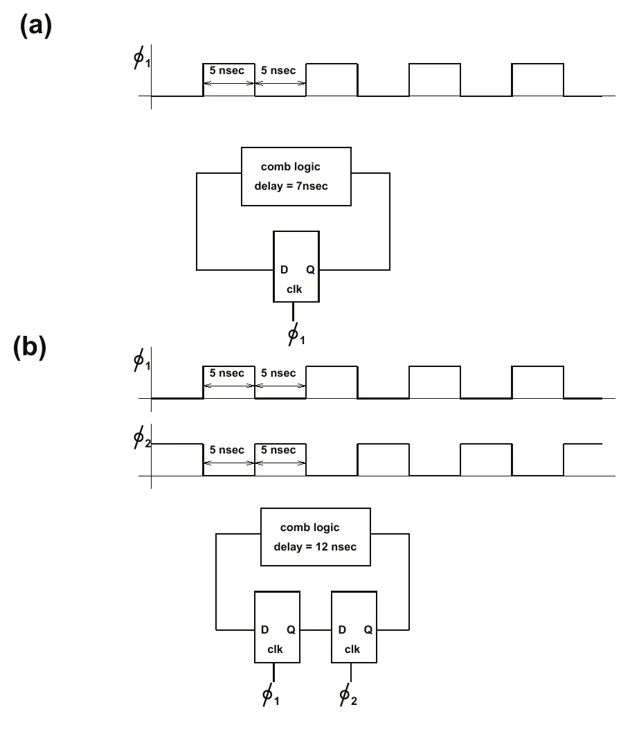
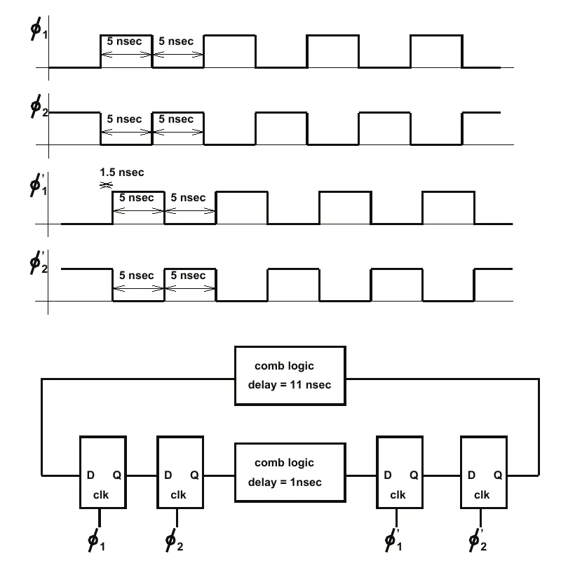
The windows. Put φ1’s rising edge at . Over each 10 ns cycle φ1 is open on [0, 5), φ2 on [5, 10), φ1′ on [1.5, 6.5) and φ2′ on [6.5, 11.5), repeating every 10 ns. Setup, hold and the latches’ delays are zero.
Part (a): one latch in a 7 ns loop
PS5-Q1a, p1. (a) [One latch on φ1, 5 nsec high and 5 nsec low, fed back to itself through comb logic, delay = 7nsec.]
PS5-Q1a (p1, redrawn): one latch on φ1, its output fed back to its input through 7 ns of logic.
Hint
What it asks. Whether a single latch fed back through its own next-state logic is a valid FSM: one state change per cycle, no more, no fewer. The words “even if the circuit is functional, indicate any issues” ask for the margins too.
The idea. While the latch is open, its output follows its input and the loop is a combinational loop. A change made at the opening edge travels round and comes back after the loop delay. If it came back while the latch was still open, it would go round again: two state changes in one cycle, a race. If it comes back after the close, it waits for the next opening and the machine advances once per cycle. So a single-latch loop has a two-sided constraint: the loop must be slower than the open time and faster than the cycle.
Why this formula. Two conditions, with .
- The lower bound is the race check: the data leaving at the opening edge returns at , and the latch closes at . It is Chapter 14 §4’s pulsed-latch hold condition with the high time as the pulse: , here .
- The upper bound is rule 2 for a one-cycle loop: the data passes the latch once per cycle, so each lap must fit in one period, or it slips further each lap.
- Conditions. One fixed delay for the logic, so its shortest and longest paths are both 7 ns; zero latch delay, setup and hold, as the handout says.
PS5-Q1a’s loop walked, computed from its values added: the data leaves as φ1 opens at 0, comes back 7 ns later at 7 ns, 2 ns after the latch closed at 5 ns, and waits for the next opening at 10 ns. Each cycle it passes the latch exactly once.
PS5-Q1a
- The launch. Because the latch opens at 0 and passes its input at once, the new state leaves at .
- The race check. Because the loop takes 7 ns, the new state returns at 7 ns, 2 ns after the latch closed at 5 ns. It cannot go round twice: no race, with 2 ns to spare.
- The wait. Because the latch is closed from 5 to 10 ns, the returned value waits 3 ns (dead time) and enters at the opening edge, 10 ns. It is now 8 ns ahead of the closing edge at 15 ns.
- Rule 2. One cycle in the loop, 7 ns of delay: . Every lap repeats lap 1, leaving at 0, 10, 20 ns: one state change per cycle. Functional.
- The issues. Because the lower bound depends on the shortest delay, the design fails if any path through the logic is shorter than 5 ns: at the fast corner the logic may be at most 28.6% faster. Because it depends on the high time too, a longer high phase breaks it; with a 50% duty cycle the period must stay in ns (at 14 ns the data returns exactly as the latch closes), so slowing the clock a lot breaks the machine. And 3 ns of every cycle is dead time.
Check. Take the high time to its two limits. As it shrinks to 0, the latch becomes an edge-triggered element: no change can come round while it is open, and only remains, Q1b’s flip-flop loop. As it grows to the whole period, the latch is always transparent and the loop is a free-running ring that changes state every 7 ns, a race on every lap. The race begins once the high time passes the loop delay, 7 ns (70% duty at 10 ns). PS5’s 5 ns high time lies below that, so the loop behaves like the edge-triggered limit, with ns to spare.
Answer: functional: the 7 ns loop is longer than the 5 ns open time (no race, 2 ns margin) and shorter than the 10 ns cycle (3 ns of slack, spent waiting). Issues: it relies on a minimum delay of 5 ns, so fast paths or a longer high phase break it (at 50% duty, ns); 3 ns per cycle is dead time. Safer: a shorter high phase (a pulse) or a master–slave flip-flop.
Remember. A single latch in a loop is a pulsed latch with its whole high phase as the pulse: the loop must be slower than the open time and faster than the cycle.
The answer key agrees
Part (b): a φ1–φ2 pair in a 12 ns loop
PS5-Q1b, p1. (b) [φ1 and φ2, each 5 nsec high and 5 nsec low; a latch on φ1, then a latch on φ2, fed back through comb logic, delay = 12 nsec.]
PS5-Q1b (p1, redrawn): a φ1 latch feeding a φ2 latch directly, the φ2 latch’s output returned to the φ1 latch through 12 ns of logic.
Hint
What it asks. Whether a φ1 latch followed directly by a φ2 latch, fed back through 12 ns of logic, works on a 10 ns clock, and if not, how to fix it in more than one way.
The idea. A φ1 latch followed at once by a φ2 latch is a master–slave flip-flop. Fed back on itself it is a one-cycle loop, and 12 ns of logic cannot fit in a 10 ns cycle. Time borrowing cannot help, because there is no second cycle in the loop to borrow from.
Why this formula. Rule 2, , with for two alternating latches. It comes from rule 1 summed round the loop: the latch openings cancel, and what is left is the loop’s total delay against its cycles. It holds whatever the launch point, so no choice of where in φ1’s window the data starts can rescue a loop that fails it. The walk shows where the failure appears. Its conditions are the handout’s: zero latch delay, setup and hold.
PS5-Q1b
- Rule 2. Because two alternating latches make one cycle, the budget is 10 ns; the loop has 12 ns. It fails by 2 ns.
- The walk. Because the φ2 latch opens at 5 ns, the data leaves it then (it cannot leave earlier) and returns to the φ1 latch at ns. φ1’s window [10, 15) closed at 15 ns: rule 1 fails by 2 ns. The φ1 latch held stale data at 15 ns. Not functional.
- Fix 1: the clock. Because the loop needs 12 ns per cycle, ns (6 ns phases): 83.3 MHz instead of 100 MHz. At 12 ns the return meets φ1’s closing edge exactly, so take a little more for margin.
- Fix 2: the logic. Speed the 12 ns block up to at most 10 ns.
- What does not work. Moving some of the logic between the two latches (3 ns and 9 ns, say) keeps the loop’s 12 ns in one cycle: rule 2 still fails. Adding another latch pair makes a two-cycle loop that holds two states at once. That is a different machine unless the FSM is redesigned.
Check. The other side, which the verdict does not rest on: the race side is safe. The data leaves the φ2 latch at 5 ns and reaches the φ1 latch at 17 ns, long after that latch’s window [0, 5) closed. The hand-off from φ1 to φ2 has zero margin (the φ1 latch closes exactly as φ2 opens), harmless here only because the 12 ns loop is far longer than any overlap.
Answer: not functional: a one-cycle loop with 12 ns of logic in a 10 ns cycle (the return reaches φ1 at 17 ns, 2 ns after it closes). Fixes: ns, or logic ≤ 10 ns. Moving logic between the latches does not help.
Remember. A latch pair fed back on itself is a flip-flop loop: one cycle, no borrowing. Rule 2 first.
The answer key agrees
Part (c): two flip-flops, 1 ns forward and 11 ns back
PS5-Q1c, p2. (c) [Latches φ1, φ2, comb logic delay = 1nsec, latches φ1′, φ2′, and comb logic delay = 11 nsec back to the first latch; φ1′ and φ2′ 1.5 nsec late.]
PS5-Q1c (p2, redrawn): latches on φ1 and φ2, 1 ns of logic, latches on φ1′ and φ2′ (1.5 ns late), and 11 ns of logic back to the first latch.
Hint
What it asks. The loop is two flip-flops, A on (φ1, φ2) and B on (φ1′, φ2′), with 1 ns of logic from A to B and 11 ns back. Is it a valid FSM with B’s clocks 1.5 ns late, and if not, which repairs work?
The idea. Rule 2 is easily met (12 ns in two cycles), but each flip-flop-to-flip-flop path has its own checks. The late B makes A → B a hold problem (a 1 ns path against 1.5 ns of skew) and B → A a setup problem (B launches 1.5 ns late into an on-time A). Both fail, and they need different cures: the hold failure cannot be fixed by the clock.
Why this formula. The two signed flip-flop checks with zero overheads, and rule 2.
- A → B, hold: with ns (B captures late): it needs ns. In latch terms, the slave of A (φ2) opens at 5 ns while B’s master (φ1′) stays open until 6.5 ns.
- B → A, setup: with ns (A captures 1.5 ns earlier than B launches): ns. That is the 1.5 ns that the late B took from this stage.
- Rule 2: 12 ns ≤ 2 × 10 ns. Necessary, but not enough: the latches’ windows decide how the 20 ns can be spent.
- Why a slower clock does not fix the race: with 50% phases, φ1′ closes at and the new data arrives at , a 0.5 ns race at any period.
PS5-Q1c’s two failures, computed from its values added. Left: data leaving the φ2 latch as it opens at 5 ns reaches the φ1′ latch at 6 ns, while φ1′ is still open until 6.5 ns (shaded): a hold race. Right: data leaving φ1′ as it opens at 11.5 ns passes φ2′ as it opens at 16.5 ns and, after 11 ns of logic, reaches φ1 at 27.5 ns, 2.5 ns after φ1 closed.
PS5-Q1c
- Rule 2. Four alternating latches give two cycles: 12 ns ≤ 20 ns. ✓
- A → B, the race. Because A’s slave opens at 5 ns, the new data reaches B’s master at ns. B’s master, φ1′, is still open until 6.5 ns on the previous state, so the new data overwrites it: hold fails by 0.5 ns ().
- B → A, the long path. Because B’s master next opens at 11.5 ns and its slave at 16.5 ns, B launches at 16.5 ns at the earliest. The return reaches A’s master at ns, but A’s window [20, 25) closed at 25 ns: it fails by 2.5 ns ().
- Fix 1: padding plus a slower clock. Because hold has no in it, pad the 1 ns path to at least 1.5 ns. Then because the long path needs , run at ns (80 MHz).
- Fix 2: padding plus faster return logic. Pad as in fix 1, and speed the 11 ns block up to at most 8.5 ns.
- Fix 3: a non-overlap window. Because the clocks may be reshaped but not deskewed, open a 0.5 ns window between φ1’s falling and φ2’s rising edge (φ1 and φ1′ falling 0.5 ns early). That cures the race, but the window is dead time for B → A: , so ns.
- Fix 4: latch design at 10 ns. Pad the 1 ns path to 2 ns (0.5 ns of hold margin), and move B’s slave latch (φ2′) 5 ns into the 11 ns block, so that the blocks are 0, 2, 5 and 6 ns. The walk: φ1′ is reached at 7 ns and opens at 11.5; φ2′ is reached at 16.5 ns, just as it opens; A is reached at 22.5 ns, 2.5 ns before it closes. It works at 10 ns, because the 11 ns of return logic now starts at φ1′‘s opening instead of φ2′‘s. The move must be at least 2.5 ns.
Check. Fix 1 in the walk model: with the path padded to 1.5 ns and ns, every latch is met and no race is flagged. And the two failures are independent: doubling the period to 20 ns leaves the race exactly as it was (it is still flagged), while padding alone leaves the 2.5 ns long-path miss.
Answer: not functional, for two reasons: a hold race from A to B (the 1 ns path is 0.5 ns too fast for the 1.5 ns late φ1′) and a long path from B to A (11 ns > 8.5 ns). Repairs: pad the 1 ns path to ≥ 1.5 ns and either slow the clock to ns or speed the return to ≤ 8.5 ns; or a 0.5 ns non-overlap window with ns; or, at 10 ns, pad to 2 ns and move the φ2′ latch 5 ns (at least 2.5 ns) into the 11 ns block.
Remember. Late skew between two flip-flops: hold fails forward, setup fails backward. Fix hold with delay, never with the clock.
The answer key agrees
Part (d): 2 ns, 11 ns and 4 ns
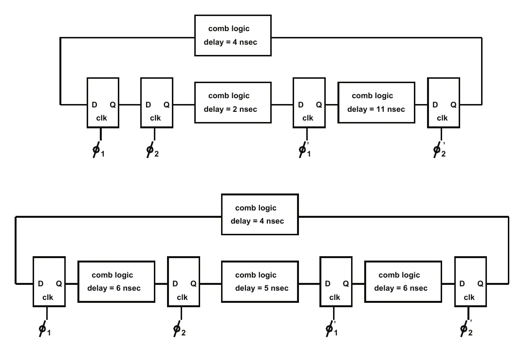
PS5-Q1d, p2. (d) [Latches φ1, φ2, comb logic delay = 2 nsec, latch φ1′, comb logic delay = 11 nsec, latch φ2′, and comb logic delay = 4 nsec back to the first latch.]
PS5-Q1d (top) and Q1e (bottom) (p2, redrawn). (d): φ1, φ2, 2 ns, φ1′, 11 ns, φ2′, and 4 ns back. (e): φ1, 6 ns, φ2, 5 ns, φ1′, 6 ns, φ2′, and 4 ns back. Both use part (c)‘s clocks, the primes 1.5 ns late.
Hint
What it asks. The same clocks, with the second flip-flop split apart: an 11 ns block now sits between φ1′ and φ2′. Does the loop work, and how can it be made to?
The idea. Rule 2 holds (17 ns in two cycles), and the 2 ns path is long enough for the 1.5 ns skew. The trouble is a single block longer than the time between the latches around it. The data cannot leave φ1′ before it opens at 11.5 ns, and φ2′ closes at 21.5 ns: 10 ns, against 11 ns of logic. A launch point cannot help, because waiting at φ1′ resets the timing to its opening edge.
Why this formula. Rule 1 along a chain that starts where the data waits. If the data waits at a latch, it leaves at that latch’s opening edge, so every later latch before the next wait needs . This is rule 1 with the arrival time written out, valid whatever happened before the wait. Here it gives two deadlines from φ1′‘s opening at 11.5 ns: φ2′ closes at 21.5 ns (so the 11 ns block must be ≤ 10 ns), and φ1 closes at 25 ns (so 11 + 4 ns must be ≤ 13.5 ns, that is, the block ≤ 9.5 ns). Rule 2 is necessary but says nothing about this distribution.
PS5-Q1d walked, computed from its values added: the data waits at φ2 until 5 ns, reaches φ1′ at 7 ns (0.5 ns after its window closed, so no race) and waits there until φ1′ opens at 11.5 ns. After the 11 ns block it reaches φ2′ at 22.5 ns, 1 ns after φ2′ closed at 21.5 ns.
PS5-Q1d
- Rule 2. Two cycles, ns. ✓
- The race into φ1′. Because φ2 opens at 5 ns, the data reaches φ1′ at 7 ns, just after φ1′‘s previous window closed at 6.5 ns: no race, but only 0.5 ns of margin.
- The wait. Because φ1′‘s next window opens at 11.5 ns, the data waits 4.5 ns there.
- The failure. From 11.5 ns the 11 ns block reaches φ2′ at 22.5 ns, after its closing edge at 21.5 ns: rule 1 fails by 1 ns. A later launch could only make the arrival later. Not functional.
- Fix 1: faster logic. Because both deadlines start from 11.5 ns, the block must be at most 9.5 ns (10 ns meets φ2′ exactly but then reaches φ1 at 25.5 ns, after its close at 25).
- Fix 2: move φ1′ into the block (retiming). Moving the φ1′ latch ns into the 11 ns block turns the blocks into and . For the data still waits at φ1′ and reaches φ1 at ns, so . At (blocks 6.5 and 6.5) the data reaches φ1′ at 11.5 ns, just as it opens, with no waiting, φ2′ at 18 ns (3.5 ns of margin) and φ1 at 22 ns (3 ns). Any from 4.5 to 6.5 ns gives the same smallest margin, 3 ns at φ1; beyond 6.5 ns φ1′‘s own margin, , becomes the smaller.
- Fix 3: a slower clock. At period , φ1′ opens at , φ2′ closes at and φ1 at . The two deadlines need and : both give ns (90.9 MHz), with zero margin at both latches. At 12 ns the margins are 1 and 1.5 ns.
Check. The walk model at 11 ns meets φ2′ and φ1 exactly (margins 0 and 0) and fails at 10.9 ns. Speeding the block to exactly 10 ns satisfies φ2′ and fails φ1 by 0.5 ns: the second deadline is the binding one.
Answer: not functional: the 11 ns block between φ1′ (opening at 11.5 ns) and φ2′ (closing at 21.5 ns) has only 10 ns. Fixes: logic ≤ 9.5 ns; or move the φ1′ latch at least 1.5 ns into the 11 ns block (4.5 to 6.5 ns gives the largest margin, 3 ns); or ns. Issue: the 2 ns path has only 0.5 ns of hold margin against the skew.
Remember. After a wait, the clock restarts at that latch’s opening edge: add the blocks from there to each later closing edge. A total that fits rule 2 can still fail locally.
The answer key agrees
Part (e): a 21 ns loop in two cycles
PS5-Q1e, p2. (e) [Latch φ1, comb logic delay = 6 nsec, latch φ2, delay = 5 nsec, latch φ1′, delay = 6 nsec, latch φ2′, and delay = 4 nsec back to the first latch.]
Hint
What it asks. Four separated latches with every block under one cycle, and the last two latches on primed clocks (visible on the page render). Does it work, and how can it be made to?
The idea. Every block is short, and the first lap meets every closing edge. But the loop holds 21 ns of logic in 20 ns of clock. Each lap therefore ends 1 ns later than the one before, and the borrowed time runs out after a few laps. This is the case rule 2 exists for: the failure is invisible in one lap.
Why this formula. Rule 2, , here 21 ns against 2 × 10 ns. Summing rule 1 around the loop cancels the latch openings and leaves exactly this, so no launch point and no partition of the same logic can avoid it. The walk over several laps shows where the failure appears. The race checks (from each latch’s opening to the next latch’s previous closing) are all safe here; the smallest is 3.5 ns, at φ1′.
PS5-Q1e lap by lap, computed added: is the margin, in ns, by which the data reaches the φ2 latch before it closes on lap . With ns the loop’s 21 ns of logic takes 1 ns more than its 20 ns of clock, so each lap ends later and the margin shrinks (4, 2.5, 1.5, 0.5) until it goes negative on lap 5. With ns it settles at 3.5 ns.
PS5-Q1e
- Rule 2. Two cycles, ns. It fails. Nothing but more time or less logic can fix it.
- Lap 1. Launched at 0: φ2 at 6 ns (open, passes), φ1′ at 11 ns (it opens at 11.5, a 0.5 ns wait), φ2′ at 17.5 ns, φ1 at 21.5 ns (open, passes). Every closing edge is met, but the lap ends 1.5 ns after φ1 opened.
- The slip. Because no latch waits after lap 1, each lap takes the full 21 ns. The departures from φ1 move from 1.5 to 2.5, 3.5 and 4.5 ns after its opening, and φ2’s margin shrinks from 4 to 2.5, 1.5, 0.5 and then −0.5 ns. On lap 5 the data reaches φ2 at 90.5 ns, after it closed at 90 ns: rule 1 fails. Not functional.
- Fix 1: the clock. Because rule 2 needs , ns (95.2 MHz). At 10.5 ns the loop settles: from lap 2 on, the data leaves φ1 1 ns after it opens, every lap takes exactly 21 ns, and φ2’s margin stays at 3.5 ns.
- Fix 2: the logic. Remove 1 ns anywhere in the loop, for example the return block from 4 to 3 ns: 20 ns in 20, and the walk then settles at 10 ns. (Any slack beyond that buys margin.)
Check. Test the claim that rule 2 is necessary and sufficient here: at 10.4 ns the walk fails within thirty laps, at 10.5 ns it never does. The 0.5 ns wait at φ1′ on lap 1 is the only dead time, which is why the lateness only accumulates from lap 2.
Answer: not functional: 21 ns of logic in a two-cycle (20 ns) loop. The first lap looks fine, but each lap ends 1 ns later, and on the fifth lap the data misses φ2’s closing edge (90.5 ns against 90 ns). Fixes: ns, or at least 1 ns less logic around the loop.
Remember. One good lap proves nothing. Rule 2 is the steady-state check; when it fails, the walk fails eventually, however many laps it takes.
The answer key agrees
Try it: walk the PS5 loops
added Chapter 14’s loop walker with PS5’s clocks: a 10 ns cycle, the last two latches on primed clocks. Pick part (c), (d) or (e), then change a delay or the skew and watch where the data waits and which closing edge it misses. For part (c) it reports both failures: the race into φ1′ in its own line, and the long-path miss at φ1 in red.
Harder variations: latch loops
You need
The walk and its three checks (Chapter 14 §8–§9). Rule 1: arrive at every latch before its closing edge, minus . Rule 2: the loop’s logic must fit in its cycles, , with one cycle per two alternating latches. The race check: data leaving a latch at its opening edge must not reach the next latch before that latch’s previous window has closed, plus .
The chain after a wait. Where the data waits at a closed latch, it leaves at that latch’s opening edge. From there, the blocks that follow must reach each later latch before it closes. This chain, not rule 2, sets the clock when it is the tighter of the two.
Two variations added in setups no past paper uses: a six-latch, three-cycle loop with a skewed corner and real setup and hold times, and PS5-Q1c’s loop on non-overlapping phases. Each part depends on the one before. No key exists, so there is no key verdict.
Variation 4: six latches, three cycles, a late corner (about 25 minutes)
Variation 4: six latches, three cycles, a late corner
added The question. A loop of six transparent-high latches on a two-phase, 50% clock: L1 (φ1) → 3 ns → L2 (φ2) → 1.5 ns → L3 (φ1′) → 6 ns → L4 (φ2′) → 9 ns → L5 (φ1) → 3 ns → L6 (φ2) → 6 ns → back to L1. L3 and L4 sit in a corner of the die whose clock arrives 1 ns late. Every latch has ns and ns; the latches add no delay. (a) What period does rule 2 allow? (b) Check every latch for a race. (c) Walk the loop at ns from L1’s opening edge. Does it work? (d) Find the smallest period that works, and explain what sets it. (e) What would it be if the corner’s clock were 1 ns early, or not skewed at all?
Variation 4’s loop added: six latches in a ring, data flowing clockwise, with the logic delays between them. L3 and L4 are on the primed clocks φ1′ and φ2′ of the skewed corner. The loop holds 28.5 ns of logic over three cycles.
Hint
What it asks. A longer chain than any PS5 part, in five dependent steps: the loop’s budget, the short paths, a walk, the true minimum period and what skew does to it. Real setup and hold times make every margin count.
The idea. Rule 2 gives a lower bound on the period, but not necessarily the period. The 1.5 ns block from L2 into the late L3 is short, so it may race; and the data arriving at L3 early must wait for L3’s late opening. From there the 6 ns and 9 ns blocks have to reach L5 before it closes, and L5 is on an on-time φ1. That chain, which the late corner cuts by 1 ns, is the real limit.
Why this formula. Three relations, all from the latch walk.
- Rule 2: , because six alternating latches make three cycles.
- Race into latch k added: . A latch’s opening edge is the earliest its data can leave; the previous window of the next latch must close, and hold, before that data arrives. The margins depend only on the phase offsets, not on the period.
- The chain after a wait added: if the data waits at L3, it leaves at L3’s opening, ns, and must reach L5 by L5’s closing edge minus setup, ns: . It holds only if L4 does not make the data wait again; L4 opens at , before the data reaches it.
Variation 4
- (a) Rule 2. Because the loop has three cycles, ns.
- (b) Races. From each latch’s opening to the next latch’s previous closing, minus 0.3 ns of hold, the margins are 2.7 ns (into L2), 0.2 ns (into L3), 5.7, 9.7, 2.7 and 5.7 ns. All are safe, but the 1.5 ns path into the late corner clears it by only 0.2 ns. These margins do not change with the period.
- (c) The walk at 10 ns. The data waits 2 ns at L2 (it arrives at 3 ns, L2 opens at 5) and 4.5 ns at L3 (it arrives at 6.5 ns, L3 opens at 11). It leaves L3 at 11 ns and reaches L4 at 17 ns, 1 ns after L4 opened, so it passes, borrowing. It reaches L5 at 26 ns, but L5 closes at 25 ns and needs the data by 24.8: it fails by 1.2 ns. Rule 2 held (28.5 ≤ 30), and the loop still fails.
- (d) The real minimum. Because the data must wait at L3 and then run 6 + 9 ns to L5, the chain gives , so ns (92.6 MHz, against the 105.3 MHz rule 2 promised). At 10.8 ns the walk meets L5 with exactly the setup time to spare, and from the second lap on the data waits 3.9 ns at L3 on every lap: dead time that the late corner forces.
- (e) Other skews. Because the chain starts at L3’s opening, the skew enters it directly: for a skew . With no skew it is 10.13 ns (the walk passes at 10.14 ns). With the corner 1 ns early, the chain asks only 9.47 ns, so rule 2’s 9.5 ns becomes the limit. The race into L3 then has more room too.
Check. The walk model (latchloop.ts, with setup 0.2 ns and hold 0.3 ns) fails at 10.75 ns and passes at 10.8 ns for the late corner, and passes first at 9.5 ns for the early one. The rule-2 bound and the chain bound cross at a skew of ns: early skew larger than that leaves rule 2 in charge.
Answer: (a) ns. (b) No race; the tightest margin is 0.2 ns, into L3. (c) It fails at 10 ns: the data reaches L5 at 26 ns, 1.2 ns after its deadline. (d) 10.8 ns, set by the chain from L3’s opening through 6 + 9 ns to L5’s closing; 3.9 ns of dead time remains at L3 on every lap from the second on. (e) 10.13 ns without skew; 9.5 ns (rule 2) with the corner 1 ns early.
Remember. Rule 2 is a lower bound. When the data waits at a latch, the chain from that latch’s opening edge to the next closing edges can set the clock instead, and skew on the waiting latch enters that chain one for one.
Variation 5: PS5-Q1c on non-overlapping phases (about 20 minutes)
Variation 5: PS5-Q1c on non-overlapping phases
added The question. PS5-Q1c’s loop (φ1 → φ2 → 1 ns → φ1′ → φ2′ → 11 ns → back; the primes 1.5 ns late; no setup, hold or latch delay), but the clock generator now makes non-overlapping phases: each phase is high for 40% of the cycle, so at 10 ns there is a 1 ns gap after each; the duty stays 40% at any period, so the gaps scale with it. (a) Write the four windows. (b) Is part (c)‘s race cured? (c) Does the loop work at 10 ns? (d) What period does it need, and how does that compare with padding the 1 ns path on 50% phases? (e) At 10 ns, how far must the φ2′ latch move into the 11 ns block, and where is the margin largest?
Hint
What it asks. Whether Chapter 14’s non-overlap window, applied to a whole latch loop, repairs PS5-Q1c, and at what price, compared with the padding repair. Then a retiming that recovers the 10 ns clock.
The idea. Shortening each phase to 4 ns makes φ1′ close at 5.5 ns instead of 6.5 ns, before the 1 ns path delivers new data at 6 ns: the race is cured without padding. But every window also closes 1 ns earlier, and the 11 ns return from φ2′ (opening at 16.5 ns) must now reach φ1 by 24 ns instead of 25 ns. The window is dead time, and the long path pays for it.
Why this formula. The same three checks with shorter windows.
- Windows: each latch opens where it did and closes later (40% duty at every period, as the question says).
- Race into φ1′: φ2 opens at , and the data arrives 1 ns later; φ1′‘s previous window closes at . At 10 ns: 6 against 5.5 ns.
- The chain: the data cannot leave φ2′ before it opens, at , and must reach φ1 by its closing edge at : , so .
- With 50% phases and padding, the same chain closes at : , part (c)‘s fix 1.
Variation 5’s clocks, computed added: each phase is high for 4 ns of the 10 ns cycle, with a 1 ns gap after φ1 falls and after φ2 falls; the primed clocks are the same waveforms 1.5 ns late. φ1′ now closes at 5.5 ns, and φ1 at 4 and 14 ns.
Variation 5
- (a) The windows. φ1 is open on [0, 4), φ2 on [5, 9), φ1′ on [1.5, 5.5) and φ2′ on [6.5, 10.5), repeating every 10 ns.
- (b) The race. Because φ1′ now closes at 5.5 ns and the new data reaches it at ns, there is no race: 0.5 ns of margin, without padding.
- (c) At 10 ns. Because φ2′ opens at 16.5 ns, the return reaches φ1 at 27.5 ns, and φ1 closed at 24 ns: it fails by 3.5 ns, a full nanosecond worse than on 50% phases (2.5 ns).
- (d) The period. ns (72 MHz). Padding the 1 ns path to 1.5 ns on 50% phases needs only 12.5 ns (80 MHz). For this loop the window is the more expensive repair, because it takes time from every window, including the one the long path needs.
- (e) Retiming at 10 ns. Moving the φ2′ latch ns into the 11 ns block makes the blocks 0, 1, and . The data leaves φ1′ at its opening, 11.5 ns. For it waits at φ2′ until 16.5 ns and reaches φ1 at ns, so (margin ). For it reaches φ1 at 22.5 ns (margin 1.5 ns), while φ2′ itself, closing at 20.5 ns, keeps a margin of . The margin is largest, 1.5 ns, for ns.
Check. The walk model with 40% windows passes at 13.9 ns and fails at 13.8 ns; with the φ2′ latch moved 3.5 ns it passes at 10 ns and with 3.4 ns it fails. Compare part (c)‘s fix 4, on 50% phases: there the latch had to move only 2.5 ns, because φ1 closed 1 ns later.
Answer: (a) φ1 [0, 4), φ2 [5, 9), φ1′ [1.5, 5.5), φ2′ [6.5, 10.5) ns. (b) Yes: φ1′ closes at 5.5 ns, before the new data arrives at 6 ns. (c) No: the return misses φ1 by 3.5 ns. (d) ns, against 12.5 ns for padding on 50% phases. (e) At least 3.5 ns; 5 to 7.5 ns gives the largest margin, 1.5 ns.
Remember. A non-overlap window is dead time in every window. It cures races without padding, but a loop with a long path pays for it at every latch.