H4. Homework 4: stick layout, gain-based design and CPL
Homework 4 is the course’s practice for three midterm families at once: reading and drawing stick layouts, sizing a path by its gains under a limit on the input capacitance, and pass-transistor logic with restoring PFETs. All of it is in the midterm’s scope (Lectures 7–10). Some parts ask for Cadence work: a Virtuoso layout, DRC and LVS, simulations. There is no simulator here, so those parts are explained as methods, and no simulated number on this page is invented.
Every answer below is re-solved; none is copied from the answer key. Where the key disagrees, the folded note on the key at the end of the part explains why, and the table at the end lists them all.
After this page you can:
- draw a stick diagram for a chain of gates and estimate each stage’s delay from and ;
- design a multi-level static CMOS gate for minimum delay under an input-capacitance limit, with the path effort, the branches and a retuning step;
- lay a complex gate out along an Euler path and say what the layout adds to the delay estimate;
- trace complementary pass-transistor (CPL) gates, build a full adder from them, and say what cross-coupled PFETs restore and what they cost.
Before you start
How to use this page. The sections follow the homework: Problem 1 (p1), Problem 2 (p2–3) and Problem 3 (p4–6). HW4-2a, p2 is Homework 4, problem 2, part (a), physical page 2 of the solution PDF. The three families are taught in full on the midterm pages, so the first part of each problem links its family’s How to approach section and says what the homework adds. Then every part is worked the same way: what it asks, the idea behind the method, the solution in steps (each step gives its reason first), a check on the result, the answer, and one thing to remember. Try each part on your own first; open the Hint if you are stuck, and step through the solution before you press “Show all”. The answer key’s verdict is folded at the end of each part. The parts that need Cadence say what the bench holds fixed, what it changes, which node to watch and how the reading becomes a number.
| Problem | Parts | Family | Chapters | Midterm pages |
|---|---|---|---|---|
| 1. Three inverters | 1a stick, 1b delay | stick layout; delay from R and Cg | 7, 9 | M5, M3 |
| 2. A four-input XOR | 2a–2f | path sizing with an input limit | 7, 8, 9, 10 | M4 |
| 3. CPL | 3a–3c | pass-transistor logic, half latches | 10, 11 | M5 |
Conventions
- The technology. The key uses the IBM 90 nm numbers “from HW3”: , and , and so does this page. The key adds that any values in the right ballpark earn credit; the Homework 3 key itself measured 0.875 fF/µm, 2.78 and 5.69 kΩ·µm, and H3 finds those two resistances twice too large for its own bench (about 1.4 and 2.8 kΩ·µm). Results in τinv don’t depend on these values; only the picoseconds scale with them.
- The delay model (Chapter 7, Section 7): a device of width driving takes , with 1 kΩ × 1 fF = 1 ps; only gate capacitance counts; no 0.69 factor. Then . (, close enough to the lecture’s 2 that every gate is sized for .)
- Loads as widths. At 0.833 fF/µm, 50 fF is 60 µm of gate (60.02; the key’s rubric uses 60).
- Gains (Chapter 8, Section 1): a stage’s gain is the capacitance it drives over its normalized inverter’s input, for an NFET-equivalent width ; the path delay is times the sum of the gains.
1. HW4-1: three inverters, laid out and timed
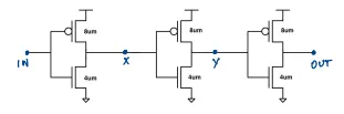
HW4-1, p1. Complete a DRC-clean, LVS-clean layout of the circuit shown above. Assume minimum length devices. Create a stick layout first before going to Virtuoso. Please turn in both your stick diagram as well as a print of your layout. From your layout and the numbers you calculated in Problem 1 [of Homework 3], estimate both and for the second inverter (loaded by the third). Compare your results with simulation of the extracted layout, using a “reasonable” slew for the input of the first inverter.
HW4-1a: the stick diagram
Hint
What it asks. A stick diagram of the three-inverter chain, the step before the Virtuoso layout: six transistors, two rails, and the wiring that carries X and Y from each output to the next input. The word “stick” decides what you draw: one line per layer, no widths.
The idea. These are the reading rules of M5’s stick-layout section, run backwards. There you find the transistors and nets in a drawing; here you place them. Each reading rule becomes a drawing rule (Chapter 9, Section 10):
- a transistor is where a poly line crosses a diffusion line, so each inverter needs one poly that crosses a p line (its PFET) and an n line (its NFET);
- only a contact joins two layers, so every connection from metal to a source, a drain or a poly needs one;
- metal that merely crosses another line touches nothing, so the output wires may pass over other lines.
Start from the lecture’s stick diagram of one inverter: a line for each diffusion, a line for the poly gate, metal lines, and a cross for each contact. Then repeat it.
Three inverters in sticks
- Share the rails. All three inverters need and ground, so draw three copies side by side under one rail at the top and one ground rail at the bottom. Each copy has a p-diffusion line (the PFET), an n-diffusion line (the NFET) and one poly line crossing both: six transistors.
- Tie the sources to the rails. An inverter’s PFET source sits at and its NFET source at ground, so each copy’s left diffusion ends get a contact and a metal drop to their rail.
- Join the drains: that is the output. Both drains are the output node, so the right ends get contacts, joined by a vertical metal line: X, then Y, then OUT.
- Carry each output to the next gate. X is the second inverter’s input and Y the third’s, so each output runs on in metal to a contact on the next inverter’s poly. IN reaches the first poly the same way.
Check. Read the drawing back the way M5 reads an exam’s sticks. Each poly crossing a diffusion is one transistor: six. Each inverter has one PFET from and one NFET from ground to its output. And OUT = NOT(NOT(NOT IN)) = NOT IN. The figure passes the same test in Chapter 9’s stick model.
Answer: the stick diagram above. The widths (8 µm and 4 µm) don’t appear in a stick diagram; they set the lengths of the diffusions in the real layout.
added Fingers. An 8 µm PFET is below the 10–15 µm at which the lecture splits a device into fingers (Chapter 10, Section 3), so one finger each is fine. The Virtuoso layout, its DRC and LVS runs and the print are tool work; Chapter 9, Section 6 says what each check proves.
Remember. Drawing sticks is reading them backwards: a crossing for every transistor, a contact for every connection, shared rails. Draw one cell, then copy it. The midterms ask the reverse (M5, MT24-4).
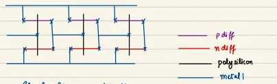
The answer key agrees
HW4-1b: the delay of the second inverter
Hint
What it asks. The rising and falling delays of the second inverter, the one that drives Y. The words “loaded by the third” decide the load: the third inverter’s input and nothing else. Then a comparison with a simulation of the extracted layout, which is a method here, since there is no simulator.
The idea. This is the single-gate delay of M3’s gate-delay section. What is new is the unit: the key’s 90 nm numbers turn the delay into picoseconds instead of a multiple of . The conducting transistor acts as a resistor , with in kΩ·µm and its width, that charges or discharges the load (Chapter 7, Section 7):
It holds with only gate capacitance in and no 0.69 factor (the page’s conventions); 1 kΩ × 1 fF = 1 ps. The PFET carries the rising edge () and the NFET the falling one ().
The comparison is a simulation bench (H3’s bench section). It holds the circuit as laid out, with every parasitic the extraction finds, and drives IN with a ramp. The node to watch is Y, timed from X, 50% to 50%, once per edge. The reading is the delay itself, so you set it beside the estimate.
t_pLH and t_pHL from R and C_g
- The load. The second inverter drives only the third one’s input, which is wired to both its gates: of gate, so .
- Rising output. The 8 µm PFET pulls Y up, so use its resistance: .
- Falling output. The 4 µm NFET pulls Y down: .
- Recognize the FO1 delay. The second inverter drives a copy of itself, so its width cancels: .
Comparing with the extracted layout (method only)
- List what the estimate leaves out. The extracted netlist carries every capacitance the layout draws, and the estimate only the third inverter’s gate. Two more loads sit on Y. The first is the drain junctions of the second inverter itself, its PFET’s and NFET’s drains (Chapter 5, Sections 5–6). The Homework 3 key’s diffusion readings (its HW3-1c: 0.5 to 0.73 fF/µm, by device and edge) put about 6 to 9 fF on 12 µm of drain, next to the 10 fF of gate. The second is the metal from Y to the third poly, and the poly itself.
- Predict the direction. The delay grows in proportion to the load, so expect the extracted simulation to be noticeably slower than 8 ps, perhaps by 1.6 to 1.9 times from the drains alone.
- Set up the bench. added A real inverter never sees a step, so drive IN with a ramp of a typical slew (Homework 3’s benches use about 2 FO4). The first inverter is there to give Y’s driver a realistic input slew, which the RC estimate ignores.
- Read it. The delay model measures from one 50% crossing to the next, so read the 50%-to-50% delay from X to Y, once for each edge. Each is or directly, so divide it by the estimate to see how much the layout added.
Check. The two edges come out within 1.6% of each other, as two FO1 delays should: ps falling and ps rising. They would be equal if were exactly , the ratio the 8/4 sizing assumes; it is 1.97.
Answer: and .
Remember. A stage’s delay is with the device that carries that edge, and an inverter driving a copy of itself takes whatever its size. Extraction only adds capacitance, so the simulated delay comes out longer than the estimate.
Check yourself The same chain with every inverter twice as wide (16 µm/8 µm). What does the estimate give for the second inverter, and what changes in the extracted simulation?
The estimate doesn’t change: the load doubles to 20.0 fF and the resistances halve, so is still . In the extracted netlist the drain capacitance doubles too (it scales with width), but the wire from Y to the next poly does not, so the wider chain comes a little closer to the estimate.
The answer key agrees
It prints 7.99 ps for ; , which rounds to 8.00. It gives no comparison with the extracted layout.
2. HW4-2: a four-input XOR, designed by gain
HW4-2, p2. This is a design problem. Please design a four-input XOR gate using our IBM 90-nm technology. Your design must drive 50 fF of load and present no more than 50 fF of capacitance on any input. Design the fastest XOR gate you can using complementary CMOS logic that meets these constraints. You may use any gate complexity and any number of level of logic, but remember that you are trying to minimize the delay. Assume that all the inputs arrive at the same time.
(a) First create a schematic of your design and do a rough sizing using gain-based tuning techniques we described in class. Use layout-dependent device models in your schematic. (b) Estimate the delays from each input to output using the technology characterizations you have done previously for IBM 90 nm. (c) Simulate your design, looking at the delays from each input to each output. Use inverters at the inputs in your simulation to simulate “typical” slews. (d) Create a stick layout of your design. Estimate its area. (e) Create a complete layout in Virtuoso of your design. Verify that it is DRC and LVS clean. (f) Extract your layout and simulate the delays again from the extracted view. Comment on any discrepancies.
This is an open-ended design: many designs meet the limits, and the key accepts “other logical equivalents sized with similar delay based sizing”. Below is one design, worked with every number checked, then compared with the key’s. The method is the point: M4’s path sizing, and in particular MT21-5a, whose input limit is also the whole design constraint.
The limits in microns. Gains are ratios of gate widths, so convert both limits first. The output drives 50 fF = 60 µm of gate. Each input may present at most 60 µm. So is at least 1, and exactly 1 when an input uses its whole allowance: almost all the path effort is logical effort and branching. A small means few stages (Chapter 8, Section 4).
HW4-2a: choosing the gates
Hint
What it asks. A schematic and a rough sizing “using gain-based tuning techniques”. So choose the gates first (this heading), then size them (the next). “Complementary CMOS logic” rules out pass transistors, and “the fastest … that meets these constraints” makes it a minimum-delay problem under two capacitance limits.
The idea. This is M4’s path-sizing question with the circuit left to you. Each stage takes times its gain, the load it drives over its normalized inverter’s input, and the path takes the sum. Two things make a topology fast here: few stages, because is small, and a small logical effort per stage, which means short stacks. What is new, compared with M4’s questions: every XOR needs both polarities of its inputs, and the inputs arrive in one. So each input must also drive an inverter, and that inverter shares the input’s 50 fF limit. The input is a branch, and the path effort depends on how the limit is split. The sizing deals with that.
Which gates?
- One gate for all four inputs? It would be one stage, but too heavy a one. A complementary XOR of four inputs has eight product terms in each network, each a stack of four. By the stack rule (Chapter 7, Section 8) four in series act as one device of a quarter the width, so each NFET is and each PFET . Every input appears in four branches of each network: one input pin is against a normalized input of , so per pin. And four-high stacks are what the lecture says to break up (Chapter 8, Section 10).
- Two levels of two-input XORs. XOR is associative, so , and two-input gates keep the stacks two high. A two-input XOR in complementary CMOS is an AND-OR-invert gate (Chapter 7, Section 5): . With NFETs and PFETs its normalized inverter is (input ), and one pin is : g = 2 per pin, the AOI22 of Chapter 8’s check.
- Complements without a stage between the levels. The second-level XOR needs both and its complement. Inverting would put an inverter on the path. Instead, build the complement in parallel at the first level: an XNOR is the same AOI22 with and swapped. Then no inverter sits between the levels, and the only inverters are at the inputs, which arrive in one polarity only.
The design: four input inverters, four first-level gates (, , , ), and one second-level XOR, .
Layout-dependent device models (method only). Part (a) asks for them in the schematic: once the layout is planned (part d), label each transistor’s source and drain as bordered, abutted or shared, so that the schematic simulation already uses the junction capacitance the layout will have (Chapter 10, Section 2). Part (d) below gives the letters for the XOR2 cell.
HW4-2a: sizing by gain-based tuning
Name the normalized-inverter NFET widths: for the input inverters, for the first-level gates, for the last gate. All four inputs are alike, so take A.
The gains, the paths and the input limit
- Start at the input, because it is the branch point. A goes to the A pin of the XOR and of the XNOR, , and to its inverter, . The limit: .
- The slow path runs through the inverter, because it has one more stage. The inverter drives the pins of both first-level gates: gain .
- A first-level gate has one pin of the last gate as its load: gain .
- The last gate has the 60 µm load: gain .
- The direct path (A straight into the first level) has only the last two gains, so it is always shorter. Size for the slow one.
- The path effort. Multiply the three gains: the inner widths cancel, and . In Chapter 8’s terms: , a branching effort of 2 at the inverter (it drives two pins, one on the path), and (Chapter 8, Section 8).
is not fixed: it depends on how much of the 60 µm goes to the inverter. The input is a branch point, shared by the inverter (on the slow path) and the first-level pins (which set the rest of the path).
First cut: equal gains, the whole input used
- Use the whole limit, with equal gains. A larger input means a smaller and so a smaller , as in MT21-5a; and with fixed, one gain for all three stages gives the smallest sum (Chapter 8, Section 3).
- Size back from the load, because the load is the one capacitance known at the end (Chapter 8, Section 6): , then , then .
- Let the input limit fix f, because it is the one condition left: becomes , that is .
- Solve it. Its root is (check: ).
- Put f back into step 2 for the widths: , , . The pins take of the input and the inverter .
- The delay: .
Retune: move input capacitance from the pins to the inverter
- Why equal gains aren’t the end. They are the best only when is fixed, and here depends on the split. A smaller frees input capacitance for the inverter, which speeds up the first stage at the cost of the other two: the lecture’s situation of a branch, retuned by inspection (Chapter 8, Section 9).
- Keep one width free. Choose . The inverter should use the rest of the input, so , and the first gain is .
- Balance the pair after it. Nothing branches between the last two stages, so for a given their product is fixed, , and equal is best: each (M4’s pair rule).
- Write the delay as a function of added: in .
- Try a few, as the lecture retunes by inspection. : 9.71 (the first cut). : 9.09. : 8.85. : 8.80. : 8.83. : 9.00. Take . added What balances there: moving a little input capacitance from the pins to the inverter speeds the first stage by as much as it slows the pair. With a larger the inverter starves and its gain climbs steeply; with a smaller one the pair’s gains climb.
- Read off the widths. , so ; round to . The inverter gets : .
| Gate | Devices | One input pin | Gain on the slow path |
|---|---|---|---|
| input inverter (×4) | PFET 16 µm, NFET 8 µm | 24 µm | |
| first level, XOR2 and XNOR2 (×4) | NFETs 6 µm, PFETs 12 µm | 18 µm | |
| second level, XOR2 (×1) | NFETs 11 µm, PFETs 22 µm | 33 µm |
Check. The three gains multiply to , which is with , as the path effort says they must. And the first cut is the special case of the retuning formula: both give 9.71.
Answer (a): the circuit above with these widths. Each input presents , within the limit. 48 transistors. The slow path has gains 1.50, 3.67 and 3.64: 8.80 τinv, against 9.71 for the equal-gain first cut. The exact minimum of this circuit is 8.80 as well (at ).
Is three stages right? added With these sizes . Chapter 8’s rule of thumb, about stages, gives , and the two big gains sit in the lecture’s 3–4 range. One more stage (make the last gate an XNOR and add an output inverter, so the polarity stays right) gives 8.54 τinv after the same retuning, 3% less: the minimum is shallow, and either design is a good answer.
Remember. When an input also feeds its own inverter, the input limit is shared, and the input is a branch. Write the delay as a function of the split, balance the stages that have nothing between them, and try a few values. In an XOR tree, make each complement in parallel (an XNOR beside the XOR), not with an inverter between the levels.
The answer key differs
It designs a different tree, with an inverter for every complement at both levels, and sizes it as if nothing branched. The key’s design, after part (f), compares the two.
HW4-2b: the delay from each input
Hint
What it asks. The delay from each input to Y, in picoseconds, “using the technology characterizations”. The words “from each input” mean every path from an input, not only the one you sized.
The idea. A path’s delay is times the sum of its stages’ gains (Chapter 8, Section 2), and here ps from the key’s numbers (the conventions; no 0.69 factor). Each input reaches Y along two paths: through its inverter (three stages) and straight into the first level (two stages). Y settles only when the later of the two arrives, so the input’s delay is the slow path’s.
Delays in picoseconds
- One calculation covers all four inputs, because each input drives the same circuit: one inverter and two first-level pins of the same sizes.
- The slow path, through the input’s inverter: .
- The direct path, straight into the first level: .
- Both edges at once. Every gate is balanced for , so rising and falling are the same in this model. (With the pull-ups are 1.6% stronger than assumed.)
- What the model leaves out. These are single-input-change delays from the top of each stack; a bottom device in a stack is slower (Chapter 8, Section 10), which the simulation of (c) would show.
Check. The two paths differ by ps, which should be the inverter’s own stage: ps. ✓
Answer (b): about 70 ps from any input to Y (the path through the input’s inverter), and 58 ps along the direct path.
Remember. Delay in picoseconds is times the sum of the gains along the slowest path. When the complements come from inverters, the slowest path is the one through the inverter.
The answer key differs
It gives the formula, or , without a number. The formula is right, but with its own from the unbranched it gives (64 ps), which leaves out the branches at the input and between the levels. The key’s design, after part (f), explains why.
HW4-2c: simulating it
Hint
What it asks. A simulation of the design of (a), timing every input to the output, with inverters at the inputs “to simulate typical slews”. There is no simulator here, so this is the method and the result to expect.
The idea. A delay bench (H3’s bench section). It holds the circuit and its sizes fixed and holds three inputs constant, and it toggles the fourth. The node to watch is Y, timed from the input pin (the output of the inverter that drives it, not the ramp). The formula is the definition of a delay: , once for each edge. Each reading is then set beside the 70.4 ps of (b).
The delay bench (method only)
- Give the inputs real slews. A real gate never sees a step, so drive each input from an inverter of a typical size, with a ramp at that inverter’s input. The problem asks for this.
- Toggle one input at a time. In an XOR every single-input change toggles Y, so hold the other three and toggle one: its delay is measured alone.
- Read both edges for every input. Rising and falling can differ in simulation, so read the 50%-to-50% delay from the input pin to Y for each: four inputs, two edges.
- Compare with (b). The simulation includes what the estimate leaves out: the drain capacitance (sized by the layout-dependent labels of (a)) and real input slews.
Check. The expected direction: the simulation should come out slower than the 70 ps of (b), because it adds drain capacitance to every load and sloped edges to every stage, and the estimate includes neither. A faster reading points to a missing load, such as an output left without its 50 fF.
Remember. A delay simulation is: a realistic input slew, one input toggled with the others held, 50% to 50% from the input pin to the output, both edges. Expect it to be slower than the gain estimate.
The key has no solution or rubric for (c).
HW4-2d: a stick layout and the area
Hint
What it asks. A stick layout of the design, and an estimate of its area. The design is five copies of one AOI22 cell (as an XOR or an XNOR) and four inverters, so the work is one cell, the XOR2.
The idea. Drawing sticks is HW4-1a’s job, with one new decision: the order of the polys. Neighbouring transistors on a line share the diffusion between them. So an order of the inputs that is an Euler path of both networks lets both rows run unbroken under straight polys (Chapter 10, Section 1). An Euler path visits every transistor once, in the same input order in the pull-up and the pull-down. M5’s stick-layout reading rules then check the drawing. The area estimate isn’t taught; the key uses a formula of its own.
The XOR2 cell along an Euler path
- Write both networks, because the Euler path is read from them. The pull-down has – in series in parallel with –; the pull-up has in series with .
- Find an order that suits both. is an Euler path of both. Pull-down: ground, , an internal node, , Y, , another internal node, , ground. Pull-up: the middle node m, , Y, , m, , , , m.
- Draw the rows. Consecutive devices share their diffusion, so both rows run unbroken under four straight polys. The two internal nodes of the pull-down are series nodes that nothing else reaches, so they need no contact.
- Wire m without crossings. m has three contacts in the p row, so it needs metal. Run it in metal 1 above the row from the first contact to the middle one and below it from the middle to the last, so it never crosses Y or the drop.
- Label the junctions for (a)‘s device models (Chapter 10, Section 2), because the label tells the schematic how much diffusion each piece has: p row b, as, as, as, b (every piece contacted); n row b, aa, as, aa, b.
The whole design is five such cells (the XNORs are the same cell with and swapped) and four inverters, placed in a row on shared rails. added The last cell’s 22 µm PFETs are wider than the lecture’s 10–15 µm, so draw them as two fingers of 11 µm (Chapter 10, Section 3); likewise the inverters’ 16 µm PFETs as two of 8 µm.
The area estimate is not taught in Lecture 9 (Chapter 9’s coverage). The key’s rubric uses its own formula: each transistor is a channel plus a diffusion of length on each side, , summed over all devices, with from the design rules.
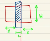
A stick layout gives a better estimate, if you want one: the cell is about one poly pitch per gate plus the end contacts wide, and one row height tall. Neither number is in the course.
Check. Read the cell back with M5’s rules. Eight crossings, so eight transistors. The pull-up is the dual of the pull-down, as a complementary gate’s must be. And Chapter 9’s stick model gives for every input (the figure’s caption).
Answer: the XOR2 cell above, in the order ; five such cells and four inverters in a row on shared rails. The area by the key’s formula, per device, summed over all devices.
Remember. Before drawing a complex gate, find an input order that is an Euler path of both networks. Then both rows run unbroken, and every neighbouring pair shares a diffusion.
The answer key agrees
Its rubric gives 1.5 points for a stick diagram “as shown in 1(a)” and 1 point for the area, by the formula per device shown above. It draws no stick layout of its own design.
HW4-2e and 2f: layout, DRC, LVS and extraction
Hint
What it asks. (e) the complete Virtuoso layout, shown DRC and LVS clean; (f) its extracted netlist, simulated again, with comments on the discrepancies. Both are tool work, so this is the method and what to expect.
The idea. Three checks, each with one job (Chapter 9, Section 6). DRC clean: the design-rule checker reports no violations. LVS clean: the transistors and connections extracted from the layout match the schematic. Extraction adds the parasitic resistance and capacitance of the drawn shapes. The bench for (f) is the bench of (c), unchanged (H3’s bench section): the same input inverters, the same toggles, the same node to watch (Y) and the same 50%-to-50% reading. Only the netlist changes, so any difference between (f) and (c) is the layout’s own load.
From layout to extracted delays (method only)
- DRC first, because the later checks assume a layout that can be built.
- LVS next, because an extracted simulation means something only if the layout is the circuit you designed.
- Extract, to turn the drawn shapes into parasitic and on each net.
- Rerun (c)‘s bench on the extracted view. Only the netlist differs from (c), so compare the delays input by input and edge by edge: each difference is the layout’s own load.
- Explain each discrepancy by where the layout added load. Expect slower edges from the wire capacitance, most on the wires that run from the first level to the last gate, and from any drain capacitance that the schematic’s layout-dependent labels did not anticipate.
Check. The expected direction: (f) should be slower than (c), never faster: extraction only adds capacitance and resistance to the same circuit. Planning the sharing in (a) is what keeps (c) and (f) close.
Remember. DRC: it can be built. LVS: it is the circuit you meant. Extraction: what the drawing adds. The extracted delays are the schematic’s plus the layout’s parasitics, so they can only be longer.
The key has no solution or rubric for (e) or (f).
The key’s design
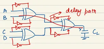
The key builds a tree of three XOR2 gates and makes every complement with an inverter, at both levels. Its sizing: (an XOR counted as , both pins of an input together), , , so , and a delay of .
The answer key differs
It gives with “B = 1 (no branching)”, and so a delay of (64 ps). Its own circuit branches twice on the delay path: each input drives its XOR pin and its inverter, and the first XOR’s output drives the last gate’s pin and an inverter (Chapter 8, Section 8). It also gives the whole 60 µm to the XOR’s input (), which leaves nothing for the inverter that the same input drives. Sized for minimum delay within the same limits, with those branches counted, the key’s tree comes to about 9.66 τinv (77 ps; gains near 1.41, 3.41, 1.41, 3.41). The design above, 8.80 τinv (70 ps), is about 9% faster, because no inverter sits between its two levels; it pays with 48 transistors against the tree’s 36. The key’s method (path effort, equal gains, the largest allowed input) is the right one, and the rubric accepts other designs.
Check yourself A classmate keeps the page's design but gives every first-level gate w1 = 4 µm. Does the design still meet the input limit? What is the largest w1 that does, and what happens to the delay as w1 approaches it?
Each input drives of first-level pins, which leaves for its inverter (): it still meets the limit. The inverter’s gain is , and the last two stages share , so at best: in all, slower than the equal-gain first cut. The limit allows any (at 5 the pins take all 60 µm and the inverter none). As approaches 5 the inverter shrinks to nothing and its gain grows without bound. The best split is near .
3. HW4-3: complementary pass-transistor logic
HW4-3, p4. One structured approach to pass-transistor logic, called complementary pass-transistor logic (CPL), takes two sets of complementary inputs into a multiplexer-like array. One set of inputs drives the transistor gates while the other group is used to drive the pass-transistor channels. The outputs are obtained through buffering inverters, which generate complementary outputs and restore full-rail voltage swings.
The lectures never say “CPL”, but the circuits are Lecture 10’s pass-transistor logic: two NFETs with complementary gates feed each node, so each node is a two-way switch (Chapter 10, Section 4). Read every node that way, with the moves of M5’s pass-transistor section and as in M5’s MT24-3.
HW4-3a: three CPL gates
HW4-3a, p4. Determine the logic functions of each of the CPL gates shown below.
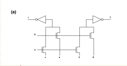
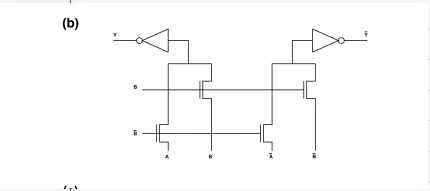
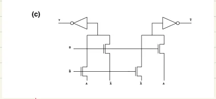
Hint
What it asks. The logic function at Y (and Ȳ) of each of the three gates. Each node drives an inverter, so the function at a label is the complement of its node’s.
The idea. The reading of M5’s pass-transistor section: each node is fed by two NFETs whose gates are complements, so exactly one of them conducts. The node is a two-way switch, “if the gate signal is 1, this input, else that one”, (Chapter 10, Section 4). Write one line per node, then follow it through its inverter. What CPL adds: every steering signal is a primary input at full rail, and only the inputs on the channels change from gate to gate. An NFET passes a 1 only up to one below its own gate (the threshold rule, Chapter 10, Section 5), so in CPL a high loses one threshold, never two.
Call the left node X (it drives the inverter that gives Y) and the right node X̄ (it gives Ȳ).
Node by node
- (a) The gates are B and , so split on B. X: gate B passes A, gate passes B. For B = 1, X = A; for B = 0, X = B = 0. So and . The right node: B = 1 passes , B = 0 passes , so it is and .
- (b) Split on B again. X: gate passes A, gate B passes B. For B = 0, X = A; for B = 1, X = 1. So and . The right node is , so .
- (c) Split on B once more. X: gate passes A, gate B passes . For B = 0, X = A; for B = 1, X = . So and . The right node is the complement, so .
- Levels. A 1 reaches X only through an NFET whose gate is a full-rail input, so the high is . A 0 passes fully, because the NFET’s source stays at 0 V. The inverters restore the swing at their outputs.
- Nothing floats or fights. The two gates of each pair are complements, so in every state each node has exactly one conducting NFET, to a full-rail input.
Check. One row of (c), straight through the switches: A = 1, B = 1. The gate-B device on the left passes , so X = 0 and Y = 1; and XNOR(1, 1) = 1 ✓. On the right, the gate-B device passes A = 1, so X̄ is high and Ȳ = 0: the complement, as it must be.
Answer: (a) , a NAND ( = AND); (b) , a NOR ( = OR); (c) , an XNOR ( = XOR).
Remember. The same switch network makes all three: only the inputs on the channels change. That is CPL’s appeal, one cell for many functions. Split each node on its gate signal, then follow it through its inverter to the label.
The answer key agrees
HW4-3b: a CPL full adder
HW4-3b, p5. Using two CPL gates, implement a full adder. One gate will generate (and ) while the other gate will generate (and ). The sum bit is , while the carry out bit is .
Hint
What it asks. A full adder from two CPL gates, one for and , one for and . The key draws both. The sum is read and checked here; the carry is built from part (a)‘s gates, and the key’s carry is checked in the note at the end.
The idea. The same reading as (a), on two levels: a first level of switches makes functions of A and B, and a second level, steered by C, chooses between them. Each output splits on C. XOR with C is “if C, the complement, else the same”, so chooses between and its complement. The majority is “if C, , else ”, so chooses between gate (b)‘s node and gate (a)‘s. Every steering signal is still an input, so a high still loses only one threshold, even through two NFETs in series. This is the structure of MT24-3’s carry, with inputs on the channels where MT24-3 has the rails.
The sum. The key’s gate is two CPL XOR stages in a row.
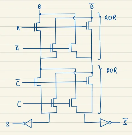
Reading the key's sum gate
- First stage, steered by A, so split on A. The left node P gets B (gate A) or (gate ), so ; the right node Q gets (gate A) or B (gate ), so .
- Second stage, steered by C, so split on C. The left output node gets P (gate ) or Q (gate C). For C = 0 it is , for C = 1 it is : it is , and its inverter gives .
- The other output node gets the opposite choice, Q (gate ) or P (gate C): , and its inverter gives .
- Levels. A 1 passes two NFETs in series, both with full-rail gates, so it loses one threshold, not two: (Chapter 10, Section 5, its first common mistake).
The sum is right: the key’s gate gives and in all eight rows.
The carry. Build it from 3a’s own gates, the way MT24-3 does.
A CPL carry
- Split the carry on C, because C will steer the second level. : for C = 0 it is , for C = 1 it is (the majority, as in MT24-3b).
- First level: reuse part (a). Gate (a) gives and ; gate (b) gives and (take the nodes before the inverters).
- Second level, a CPL multiplexer on C. Node X gets (gate C) or (gate ), so ; node X̄ gets (gate C) or (gate ), so .
- Follow each node to its label, because the inverters sit in between: X̄ through an inverter gives , X through an inverter gives . Twelve NFETs and two inverters, like the key’s.
- Levels. Every gate in the network is a full-rail input, so highs again lose one threshold, never two.
Check. Trace one row through the carry: A, B, C = 1, 0, 1. C = 1 selects the node, which is 1, so X = 1; the majority of 1, 0, 1 is 1 ✓. X̄ selects , so the two nodes differ, as they must.
Answer: the key’s sum gate, and the carry above (or the key’s carry, corrected as below). This carry is MT24-3’s network without its cross-coupled PFETs: MT24-3 passes the rails where this one passes inputs, which is the same multiplexer.
Remember. A full adder in pass logic is a multiplexer on C: the sum chooses between and its complement, the carry between and . Every steering signal is an input, so a high loses one threshold, never two.
Try every gate of this problem here: set the inputs and read each node’s level; the table runs every row.
What to notice.
- In every CPL gate each node is a 1 at (4 V at Chapter 10’s 5 V and 1 V) or a full 0, never worse: every gate signal is a full-rail input.
- “carry (key, as drawn)” (the key’s carry, drawn below the widget) at A, B, C = 0, 0, 1: X is 1 (so = 0, right) but Z is also 1, so = 0 too. The two outputs should always differ.
Check yourself The key's sum gate passes a 1 through two NFETs in series. Why does S's node reach VDD − VTn and not VDD − 2VTn? Would MT23-2's lowest high happen here?
Each NFET stops when its own reaches . Both have their gates at a full (A, Ā, C, C̄ are inputs), so the second stops at too. MT23-2’s needs a degraded node on a gate ( steering the output pair); in CPL the steering signals are always inputs, so it can’t happen (M5, MT23-2c).
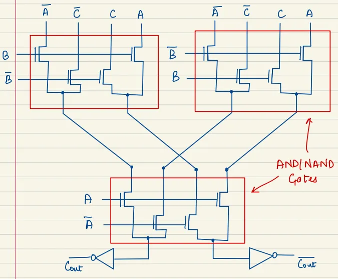
The answer key differs
It gives the carry circuit above. Its first level makes four multiplexers on B: and (left box), and (right box). Its second level makes from (gate A) and (gate ): , so the left output, , is right. But the right pair, as drawn, passes with gate and with gate A. That node is , which is not : the output labelled equals instead of its complement for A, B, C = 001, 011, 100 and 110. Swap the gates of that pair (A on the device that passes , on the one that passes ) and both outputs are right. The key’s own note, “more than one way of making the full adder”, stands.
HW4-3c: cross-coupled PFETs
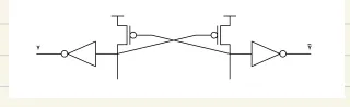
HW4-3c, p6. In some cases, cross-coupled PMOS devices are added to the output of CPL gates as shown above. What advantages and disadvantages does this lend to the circuit?
Hint
What it asks. What the two cross-coupled PFETs add to a CPL gate, for better and for worse. “Advantages and disadvantages” asks for both sides, and each one is a cause and its effect, not a word in a list.
The idea. A PFET from whose gate is the complementary node is a half latch (Chapter 10, Section 6), exactly MT24-3’s P3 and P4 (MT24-3c). It restores a high that the NFETs degraded. But by the lecture’s test, static logic works for any sizing (Chapter 10, Section 9), and a PFET that a falling node must overpower makes the gate ratioed (MT24-3a). So the advantages come from the restored high, and the disadvantages from the fight on every transition.
What the two PFETs do
- Start from the levels of 3a. In every settled state one node is a full 0 and the other a degraded (3a, step 4).
- Follow the 0 to the gate it drives. The 0 is on the gate of the PFET that feeds the other node. That PFET turns on and pulls the high node the rest of the way to . They are half latches (Chapter 10, Section 6), cross-coupled because each node already has its complement beside it, exactly as in MT24-3c.
- Gained: full swing on both nodes. The output inverters now see a full , so their PFETs turn fully off; without the latch, an input at leaves an inverter’s PFET at the edge of conduction (“the next gate may also not turn its PFET fully off”, Chapter 10, Section 5). The high noise margin is restored. The rising node also stops crawling toward : once the other node falls, its PFET finishes the edge.
- Paid: a fight on every falling edge. On every transition the node that must fall still has its PFET on (its gate is the other node, still low), so the NFETs must fight it: the falling edge is slower, current flows from to ground during the fight, and the circuit works only if the PFETs are weak enough. That is ratioed logic by Lecture 10’s test (50:43), the verdict of M5 and Chapter 10 for MT24-3a (Chapter 10, Section 9).
- Also paid: area and timing. Two more transistors per gate. And whether a transition completes is a race between the falling node and its PFET, so it depends on the sizes and on the complementary inputs arriving together.
Check. One settled state, at Chapter 10’s 5 V and 1 V. The pass network leaves the high node at V and the other at 0 V. The 0 V node is the gate of the PFET that feeds the high node, so that PFET has V and pulls the node to 5 V. The other PFET’s gate is now at 5 V, so it is off and leaves the 0 alone. The state is consistent and nothing fights: the fight happens only on a transition, which is why every disadvantage is about switching.
Answer: Advantages: full-rail (regenerated) outputs at both nodes, so the buffering inverters draw no static current and the noise margin is restored; the slow tail of the rising node is removed. Disadvantages: the gate becomes ratioed (the PFETs must be weak, or a node never falls); every falling edge is a fight, slower and with contention current; extra area; sensitivity to sizing and to when the complementary inputs arrive.
Remember. Cross-coupled PFETs on complementary nodes are half latches: they buy a full swing and pay with a ratioed, fighting falling edge. “Faster” is true only for the rising node’s tail.
Check yourself Is a CPL gate without the cross-coupled PFETs static CMOS? And with them?
Without them: each node is connected through exactly one conducting NFET to a full-rail input in every state, and nothing depends on sizing, so it is static (with degraded highs), like the pass networks of MT24-3 alone. With them: every falling transition is a fight that the NFETs must win, so correct operation depends on the PFETs being weak: ratioed, as in MT24-3a.
The answer key differs
It says “Advantages: (a) Speed. (b) Regeneration (full scale signal). (c) Some added noise tolerance. Disadvantages: (a) More area. (b) More power. (c) Contention is some latch structures (DCVS). (d) Sensitive to input timing.” The list agrees with the course, with two qualifications. Speed holds only for the rising node’s tail; the lecture’s point is the opposite edge: the pass path is “actually fighting that half-latch device”, which slows that transition (Lecture 10, 32:11). Power goes both ways: the fight adds contention current, but the restored high removes the static current of an output inverter driven at . “DCVS” (differential cascode voltage switch) is a name the lectures never use; the contention it refers to is the half-latch fight, which makes the gate ratioed.
What this means for the midterm
Where each method comes back.
- Stick layouts (HW4-1a, HW4-2d). The midterms ask the reverse: read a stick layout and give the schematic and the function (M5, MT24-4 and MT23-4; the moves are in M5’s stick-layout section). The rules are the same: each poly crossing a diffusion is a transistor, an uncontacted piece means series, only a contact connects layers. About 5 minutes.
- Delay from R and Cg (HW4-1b). and appear in every inverter-chain question (M3, for example MT23-1d and MT17-3). A minute or two.
- Path sizing under an input limit (HW4-2a–b). MT21-5a is the exam version: use the whole input allowance, compute , equal gains back from the load. HW4-2 adds the branch at the input, which is M4’s retuning: write the delay as a function of one width, balance the pairs, try a few values. 15–20 minutes for a 35–40 point question.
- Pass-transistor circuits and half latches (HW4-3). MT24-3 is a CPL carry with cross-coupled PFETs, and MT23-2 a pass-transistor full adder. The exam sequence is: static?, the function, the levels or what the PFETs do, a static CMOS equivalent (M5’s pass-transistor section). About 17 minutes.
Traps this homework sets.
- Calling a gate “no branching” when an input or an internal node also drives an inverter (HW4-2’s key).
- Equal gains when depends on the sizes: an input limit shared between two gates is a branch.
- Reading an output inverter’s label as the node’s value: in CPL, as in MT24-3, the node that computes drives the inverter labelled .
- Counting a threshold per series NFET: CPL loses one, because its gates are inputs.
- Calling cross-coupled PFETs “faster” without saying which edge: they slow the falling one.
What the key gets wrong
Re-solving every part found these disagreements; all are recorded in this page’s review/decisions.md.
| Part | The key | Here |
|---|---|---|
| HW4-2a–b | its XOR tree: with “B = 1 (no branching)”, | its inputs and first-level output also drive inverters, so ; within the limits that tree is about 9.66 τinv. The page’s design: 8.80 τinv (70 ps) |
| HW4-3b | carry circuit as drawn | right; the side’s bottom pair has A and Ā swapped, so that output is wrong for 001, 011, 100, 110 |
| HW4-3c | “speed”, “more power” | speed only for the rising node’s tail (the falling edge fights the PFET); power both ways |
| HW4-1b | 7.99 ps | 7.997 ps rounds to 8.00 (a rounding slip, no error in method) |
Every other part (HW4-1a, HW4-3a, the sum in HW4-3b, the method of HW4-2) agrees with its key after re-solving.