10. Pass-transistor and ratioed logic
Lecture 10 has two halves. The first finishes the layout material: how to order the transistors of a complex gate so that they share diffusions (an Euler path), how to tell the schematic about that sharing so its simulation sees the right junction capacitance (layout-dependent device models), and how to lay out a very wide transistor (fingers). The second half leaves complementary static CMOS behind. Pass-transistor logic uses transistors as plain switches that pass a signal from one node to another. It is compact, but it brings three problems this chapter teaches you to spot: a high level that falls short of , gates that are only static if their inputs obey a rule, and gates whose correct operation depends on how the transistors are sized. That last kind is ratioed logic. The lecture’s most memorable example is a circuit almost everyone believes is static, the six-transistor XOR. It ends with the oldest ratioed family, pseudo-NMOS.
After this chapter you can:
- find an Euler path through a gate’s pull-up and pull-down, lay the gate out with shared diffusions, and read a stick diagram back into a schematic;
- label each diffusion b, a or s and say why the schematic needs those labels;
- say when a device must be fingered and how many fingers it needs;
- trace a pass-transistor circuit’s truth table and decide whether it is static;
- explain why an NFET passes only , and fix it with complementary pass transistors or a half latch, knowing what each costs;
- state when a pass-transistor multiplexer is static (one-hot selects);
- explain why a pass transistor’s delay must be found with its driving gate, using channel-connected components;
- show that the six-transistor XOR is ratioed, and say how sizing could break it;
- explain pseudo-NMOS: its non-rail low, its static power, and why it is still used for wide NORs.
Boxes and equations marked board were written in the lecture. Parts marked added are explanations or examples this guide adds.
Before you start
You need these ideas from earlier chapters. Each is restated here.
- Static CMOS (Chapter 7). A gate is static when, for every settled set of inputs, the output is connected to exactly one of or ground. Both connected is a fight (ratioed logic); neither is a floating node (dynamic logic). Complementary static CMOS guarantees it: the pull-up and pull-down are duals, series in one where the other is parallel.
- Stacks (Chapter 7). Series stacks are slow; two high is fine, three questionable, more than three is avoided.
- Turning off (Chapter 4). An NFET conducts only while its gate is at least above its source, and the source is whichever channel terminal is at the lower voltage. A PFET conducts while its gate is at least below its source, the higher terminal.
- Sharing diffusions (Chapter 5). Sources and drains are junction capacitors. Two devices in series can share one diffusion, and if the shared node goes nowhere else it needs no contact, which makes it smaller still.
- Stick diagrams (Chapter 9). A row of PFET diffusion under the bus, a row of NFET diffusion over the ground bus, vertical polysilicon lines for the gates crossing both rows, and contacts where metal reaches a diffusion.
- Noise margins (Chapter 6). and : a degraded output level eats into them.
Notation. is NOT . The lecture’s numbers are those of Chapter 6: , , . A “pass transistor” is a transistor whose source and drain carry a data signal from one node to another, rather than connecting a node to a supply.
1. Sharing diffusions along an Euler path
The idea. If you order a gate’s transistors so that each one shares a terminal with the next, in both the pull-up and the pull-down, the two diffusion rows run unbroken and the gate polys run straight from one row to the other.

The gate
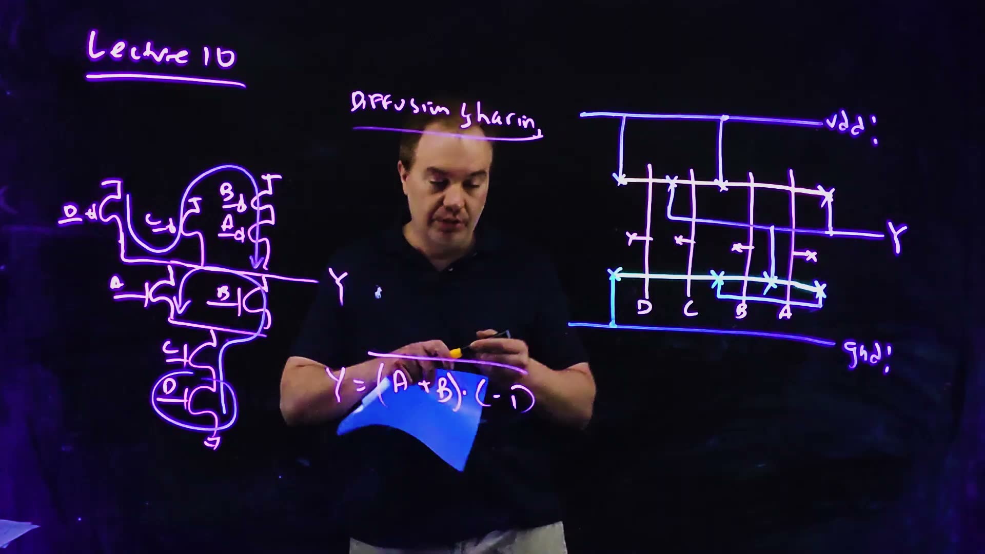
The lecture lays out a bigger complementary gate (00:14) board:
- pull-down: NFETs A and B in parallel, in series with C, in series with D, to ground;
- pull-up, the dual: PFETs D and C and the series pair B–A, all in parallel between and Y.
The pull-down conducts when is true, so
Its stack is “a little bit questionable” by Chapter 7’s rule (00:32). (The lecturer calls it “a four high stack”; the NFET stack is three high, A-or-B, C, D, and the gate has four inputs.)
The Euler path
To share diffusions, the lecturer forms an Euler path: “a path that goes through every device exactly once” (01:38), one for the pull-down and one for the pull-up. Walking along the path, each device must share a terminal (a net) with the next one; in the layout that shared net becomes one shared diffusion.
An Euler path for both networks (board, 01:38–02:53)
- Pull-down, starting at ground: D (ground to ), then C ( to ), then B ( to Y), then A (Y back to ). Each device shares a net with the next, so the order D C B A works.
- Pull-up, starting at : D ( to Y), then C (Y to ), then B ( to ), then A ( to Y). The same order, D C B A, works again.
- Because the two orders are the same, the D gate is above the D gate, the C gate above the C gate, and so on: “I’m going to be able to connect the polys between the PFET and the NFET, and it’s going to be very, very nice” (02:24). In this example the lecturer gets “a little lucky”: not every gate has one order that suits both networks.
Contacts
With the order fixed, the lecturer walks along each row deciding which diffusions need a contact (04:01–05:38) board:
- NFET row: ground contact left of D; no contact between D and C, because that node () goes nowhere else; a contact between C and B (); a contact between B and A (Y); a contact right of A ( again, wired to the C–B contact).
- PFET row: left of D; Y between D and C; between C and B; no contact between B and A (the internal node ); Y right of A.
Then the polys get their input connections, and the two Y contacts in each row are wired to the output (05:38). “The beauty here is because I was able to pick an Euler path such that all these gates lined up, I can now connect them together like this. I don’t have to jog them around” (06:04).
What to notice.
- In D C B A both rows are unbroken; the lecture’s contacts appear exactly where a net leaves the row.
- Try B C A D: the pull-down has no net in common between C and A, so the row breaks, and each break leaves two more diffusion ends to contact. Only 4 of the 24 orders are Euler paths of both networks.
- The rule for a contact added: a diffusion needs one if its net leaves the row (a rail, the output) or appears again elsewhere in the row. A node shared by two neighbours and nothing else needs none.
Reading a stick diagram back added. Past midterms give a stick layout and ask for the schematic (MT23-4, MT24-4). Run the rules backwards, one row at a time:
Stick diagram to schematic (added)
- Name every diffusion region by the net its contact reaches (, ground, Y, or a wire shared by two regions). An uncontacted region between two gates is an internal node.
- Each poly crossing a row is one transistor, connecting the regions on its two sides.
- Two devices joined only by an uncontacted region are in series. Devices whose regions are wired to the same pair of nets are in parallel.
- Write the pull-down as a switch network, check that the pull-up is its dual, and read off the function as in Chapter 7.
Check yourself An NFET row reads, left to right: a contact to ground, gate A, a diffusion with no contact, gate B, a contact to Y, gate C, a contact to ground. What is the pull-down, and what function does the gate compute if its pull-up is the dual?
A and B share only the uncontacted region, so they are in series between ground and Y. C connects Y to ground on its own, in parallel with that pair. The pull-down conducts for , so , an AOI gate. Note how C shares the Y contact with B: one contacted diffusion serves both.
Check yourself Is B C A D an Euler path of the lecture's pull-down? (A and B are in parallel between Y and n1; C joins n1 to n2; D joins n2 to ground.)
No. B (, ) and C (, ) share , but the next device, A, has terminals Y and and none of them is , so the row breaks there. D then needs , which A doesn’t have: a second break. Set the widget to B C A D to see both.
2. Layout-dependent device models
The idea. Once you have planned how the diffusions will be shared, you can tell the schematic, so that its simulation already uses the junction capacitance the layout will have.
Why
A schematic simulation needs each transistor’s source and drain junction capacitance (Chapter 5), and those depend on the layout: a shared diffusion is smaller than two separate ones, an uncontacted one smaller still (06:49). You would like that accuracy “before you actually lay it out” (07:26). If you have planned the layout, you can annotate the schematic so that it simulates “with what the real junction capacitances are going to be, taking into account the diffusion sharing that you have planned” (07:26).
How: three letters
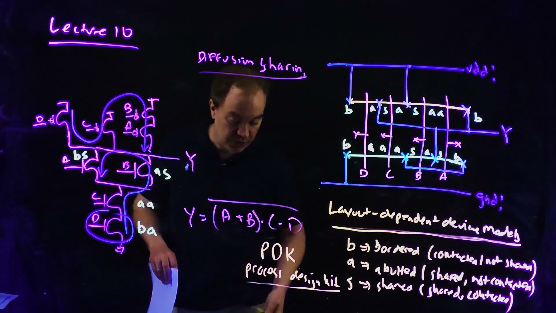
In Virtuoso, each transistor’s instance properties (press Q) start with two letters: the first describes the diffusion sharing of its source, the second of its drain (07:59). There are three letters (08:28) board:
| Letter | Name | The diffusion is |
|---|---|---|
| b | bordered | contacted, but not shared |
| a | abutted | shared, but not contacted |
| s | shared | shared and contacted |
The letters, and how they are set up, are a choice of each foundry’s process design kit (PDK) board: the set-up for the common CAD tools that a foundry gives you to use its technology (08:39–09:22). These are the IBM (now GlobalFoundries) letters; TSMC’s kits use others, but every PDK supports the idea (09:22).
Labelling the lecture’s layout
Region by region (10:45–11:58) board:
- a contacted region at the end of a row, belonging to one device, is b for that device;
- an uncontacted region between two devices is a for both, “aa”;
- a contacted region shared by two devices gets a on one side and s on the other, because its contact must be counted once: “this could be SA or AS, it doesn’t matter” (11:20).
The NFET row reads b, aa, as, as, b and the PFET row b, as, as, aa, b. Each device then takes the two letters of its own sides: the board writes D = ba, C = aa, B = as, A = bs (12:25–13:12). With those labels in the schematic, the simulator computes each source and drain area and perimeter to match the layout, and you get “a very accurate estimate in schematic before you even do layout of what the delay of this is going to be” (13:13). The catch: you have to plan the layout while you draw the schematic (13:49).
The widget of Section 1 labels every order you try.
Common mistakes.
- Thinking the letters describe the device. They describe the diffusions on its two sides; the same transistor changes letters if the layout changes.
- Giving both devices an s on one shared contacted region. That counts its contact twice; one side is a.
Check yourself A two-input NAND's pull-down is laid out ground | A | x | B | Y, with the internal node x uncontacted. Label each region and each device.
Ground: contacted, A’s only, so b. x: shared, no contact, so aa. Y: contacted, B’s only, so b. Device A: b on its ground side, a on its x side; device B: a on its x side, b on its Y side. In the PDK’s order (source first) both read the same way round: the source of A is ground (b), of B the node x (a), so A is “ba” and B “ab”.
3. Fingers for wide devices
The idea. A transistor wider than about 10–15 µm is split into several narrower devices in parallel, the fingers, that share their diffusions.

To drive a very large load you need a very wide device (14:23). Drawn as one transistor, it is a long, thin strip of diffusion with a long poly gate and “a zillion contacts” (16:00). Two problems (16:12) board:
- The aspect ratio is terrible. “Long and skinny like this … where the hell am I going to fit this thing” (16:29).
- The gate is an RC line. The poly has resistance, and it is loaded all along its length by the gate capacitance. A gate signal switching at one end takes time to travel to the other, so “part of the transistor will turn on down here, and then there’ll be a delay before the rest of the transistor turns on” (17:02–18:00). Interconnect returns to this kind of line later in the course.
The fix board: if is more than about 10–15 µm, finger the device (18:17). Draw several gates across one diffusion and tie every other diffusion together: one set is the source, the other the drain. The result is equivalent to that many devices in parallel (18:47–20:10). The board’s example has five gates: a five-fingered device. Its fingers form an Euler path of their own.
In Virtuoso the instance properties have a number of fingers parameter: set it, and the schematic accounts for the fingered layout, and the layout tool generates the fingered device for you, fully contacted (20:26–21:25). Each finger should be no wider than about 10–15 µm (21:25).
Worked example. added A 60 µm NFET.
- At most 15 µm per finger: fingers of 15 µm.
- At most 10 µm per finger: fingers of 10 µm.
- Four fingers need five diffusions: source, drain, source, drain, source. Six need seven.
- Each finger is a parallel device: the total width, and so the drive, is still 60 µm.
Check yourself With an even number of fingers, the two outermost diffusions are on the same net. Which net should that be, source or drain, and why? (Think of Chapter 5's two parallel transistors.)
The source, which for an NFET is usually ground. The drain is the switching output; with the sources on the outside, every drain region is shared between two fingers, so the switching node carries the least junction capacitance. Chapter 5 called the opposite arrangement “the poor choice”. (Added: the lecture doesn’t discuss which net goes outside.)
4. Pass-transistor logic
The idea. Instead of connecting the output to a supply through a pull-up or pull-down network, pass-transistor logic (PTL) uses transistors as switches that pass the value of one signal through to the output. Whether the result is static depends on the inputs.
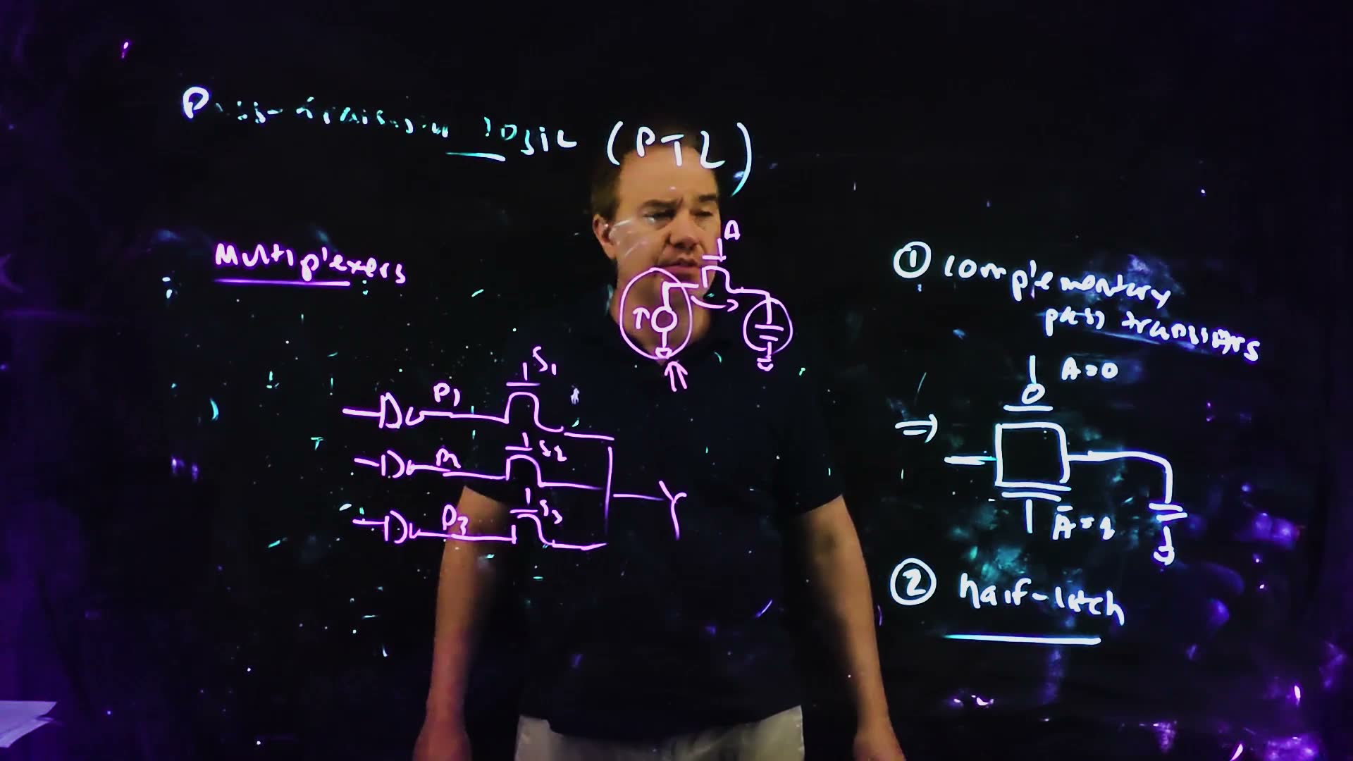
So far the course has used complementary static CMOS. Pass-transistor logic is “based on the idea of treating the transistors more generally like switches”, and it is very useful for certain logic constructs (22:16).
The lecture’s example
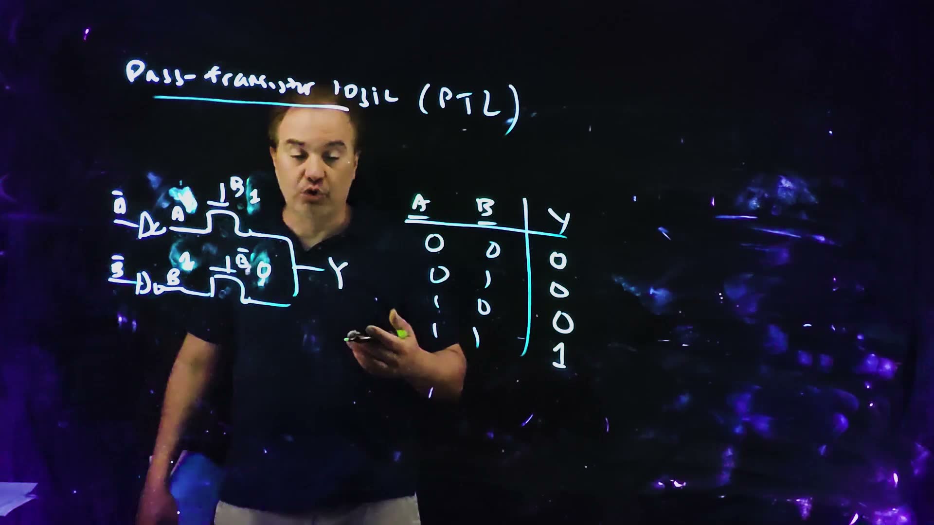
The circuit (23:12–24:14) board:
- inverters produce A (from ) and B (from ), and somewhere another inverter makes , so B and are always complements;
- an NFET with gate B passes A to the output Y;
- an NFET with gate passes B to Y.
Its truth table (board, 24:18–26:00)
- A = 0, B = 0: , so the lower NFET is on and passes B = 0. The inverter that drives B pulls Y down to 0.
- A = 0, B = 1: the upper NFET is on and passes A = 0. Y = 0.
- A = 1, B = 0: the lower NFET passes B = 0. Y = 0.
- A = 1, B = 1: the upper NFET passes A = 1. The PFET of A’s inverter pulls Y up. Y = 1.
- Y = 1 only for A = B = 1: an AND gate (the lecture doesn’t name it). Two NFETs and the inverters that the circuit needs anyway.
Is it static?
“It’s certainly not complementary, but is it static?” (26:22). Yes board: in every one of the four states there is exactly one path from Y to or ground. The path goes through an inverter, so the output sees “effectively a two-high stack”: the pass transistor and one device of the inverter (26:42).
But it is static only because B and are complements. “These two being driven by their complements are absolutely essential to ensuring that this is static” (26:59). Chapter 7’s constrained gate made the same point: once a gate leaves complementary CMOS, being static can depend on a rule about the inputs.
Try it, and the other circuits of this chapter, at switch level:
What to notice.
- In the PTL gate every node is a clean 0 or 1, except Y for A = B = 1: it is drawn as a weak 1, 4 V. That is the next section.
- The widget generates from B, so the two can’t disagree. If both gate signals were 1 with A = 1, both NFETs would conduct and A’s inverter would fight the other one (the switch model puts Y at 2.5 V): not static.
- The truth table beside the schematic settles each row from power-up (0 V everywhere) with the current sizes.
Check yourself In the PTL gate, suppose a glitch makes the gate signals B and B̄ both 1, while the inverter fed by B̄ still makes the data input of the lower pass transistor. Is there a fight with A = 1? With A = 0?
Both pass transistors conduct. The lower one carries its inverter’s output, NOT = 0. With A = 1, the upper one carries A = 1 from A’s inverter (its PFET to ) and the lower one a 0 from the other inverter (its NFET to ground): a path from to ground through Y, a fight whose outcome depends on the relative strengths. With A = 0 both carry a 0, and there is no fight. Either way the gate is static only while the complement rule holds.
5. The degraded high, and complementary pass transistors
The idea. An NFET passes a 0 perfectly but a 1 only up to , because it turns itself off as the output rises. A PFET in parallel, driven by the complementary signal, carries the output the rest of the way.
Why the high is VDD − VT
In the A = B = 1 state, “is this output going to pull all the way to ? And the answer, of course, is no” (27:39) board.
The NFET's high level (27:39–28:06; the board writes it at Y)
- The pass NFET’s gate is at . Its channel connects A’s inverter (at ) to Y, which starts low.
- The source is the lower terminal: Y. So .
- As Y charges up, shrinks.
- When , and the NFET cuts off board: the output stops there.
- With the lecture’s numbers, instead of 5 V.
Pulling down, the source is the inverter’s side, at 0 V, so stays at all the way and Y reaches ground (29:14). A logic 1 at is “not great because it degrades my noise margins” (28:06): is lower, so shrinks. The next gate may also not turn its PFET fully off.
added The PFET is the mirror image: it passes a 1 perfectly, but a 0 only down to , where its has fallen to its threshold (Lecture 11 says this at 6:45). And is the threshold model’s answer; body effect (Chapter 5) raises the NFET’s threshold as its source rises, so a real NFET stops a little lower still.
Fix 1: complementary pass transistors
Put a PFET in parallel with the NFET and drive its gate with the complementary signal (28:45) board. When the NFET’s gate is 1, the PFET’s is 0, and both conduct. Pulling down, the NFET guarantees ground; pulling up, the PFET guarantees (29:14). Both devices help in both directions; Lecture 11 uses that to size them (Chapter 11).
The cost is “significant” (29:45): an extra PFET, and with it an N well (Chapter 9’s layout), plus possibly an inverter to make the complementary gate signal. “So this comes with a large degree of overhead … and I may often decide not to do that” (30:16).
Watch the two levels form in a circuit with its driving inverter:
What to notice.
- NFET alone, Y rises: Y climbs quickly at first, then crawls; after 1 ns it is still only at 3.85 V, approaching 4 V and never passing it.
- NFET + PFET: Y reaches 5 V, and sooner (a 45 ps delay instead of 66 ps at 20 fF): the PFET keeps its full gate drive the whole way.
- Y falls: all three reach 0 V; the NFET is at its best there.
Common mistakes. added
- Counting one per series device. Two NFETs in series, both with their gates at , pass , not : each one stops only when its own reaches , and the second one’s gate is still at the full (a Fall 2026 class addition). The second drop does appear when a degraded node drives a gate: an NFET whose gate sits at passes at most .
- Calling dual-rail signals “complementary pass transistors”. A circuit that carries both and through NFETs still has weak highs; the fix needs a PFET in parallel on the same path.
Check yourself A pass-transistor multiplexer uses NFETs only, with VDD = 2.5 V and VTn = 0.5 V. What is the output high, and why?
. Passing a 1, the NFET’s source is the output; its falls as the output rises, and it cuts off when , at . (MT21-1b asks this.)
Check yourself A capacitor charged to 5 V discharges through a PFET whose gate is held at 2 V, to ground; |VTp| = 0.7 V. Where does it stop?
The PFET’s source is the capacitor side (the higher terminal). It conducts while , so it stops at : a PFET can’t pull a node below its gate voltage plus . (HW1-2b has the same structure with other numbers.)
Check yourself With VDD = 5 V and VTn = 1 V: (a) two NFETs in series, both gates at VDD, pass a 1 from an inverter to a load; (b) an NFET passes a 1 to node P, and P drives the gate of a second NFET, which passes a 1 to the load. What does the load reach in each case?
(a) 4 V: the first device stops its node at 4 V, and the second, with its gate at 5 V, can carry the load up to too. One drop, not two. (b) P reaches 4 V; the second NFET’s gate is then at 4 V, so it stops when the load reaches . This is how MT23-2c’s "" arises: the degraded node is on a gate.
6. The half latch
The idea. Restore the full high with feedback: an inverter on the output drives the gate of a small PFET from to the output. Once the output is high enough to be read as a 1, the PFET pulls it the rest of the way. The price: when the output must fall, the pull-down has to fight that PFET.
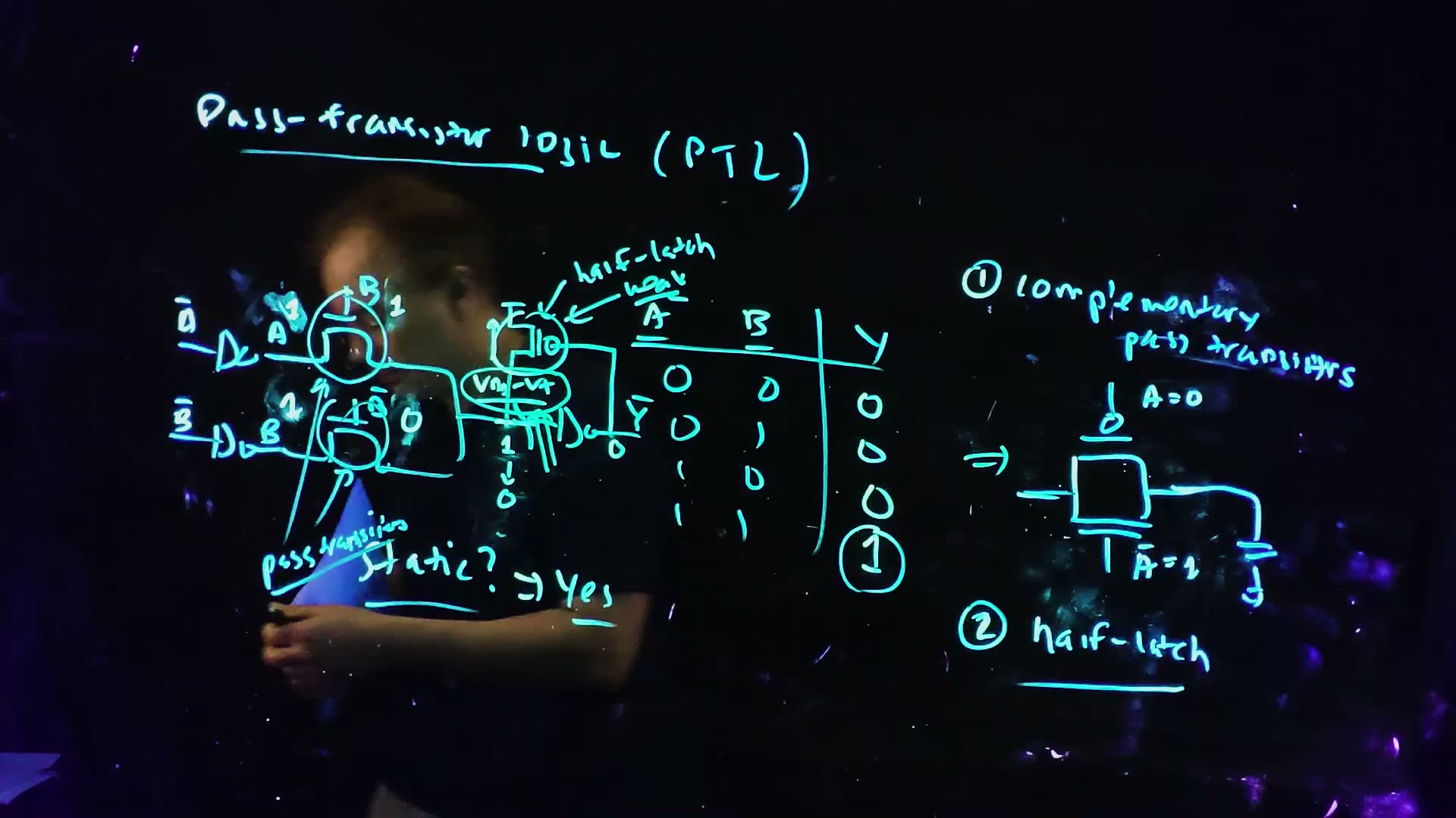
The second fix (30:32) board: take Y through an inverter to get , and wrap a single PFET around it, from to Y with on its gate. If the inverter’s NFET were there too, the two inverters would be cross-coupled: a full latch, which the course comes back to with sequential circuits. With only the PFET, it is a half latch (31:01).
How it restores the high (31:29–32:28)
- The pass NFET pulls Y up to .
- That is enough to switch the inverter (“hopefully”): goes to 0.
- turns on the half-latch PFET, which pulls Y all the way to .
- Y no longer sits at , and the next gate sees a full 1.
Why it must be weak
The half-latch PFET is “often chosen to be weak” board (31:49). When Y must go down, the PFET is still on (its gate, , is still 0), so the pass path is “actually fighting that half-latch device”: it slows one of the two transitions (32:11). The pull-down must quickly overpower it, until Y passes the inverter’s threshold, rises, and the PFET turns off.
So the half latch buys a full-rail high without complementary pass transistors, and you might choose it if you can’t tolerate the drop in your noise margins (32:28).
In the PTL gate of the widget above, choose “② half latch”, set A = B = 1, then set A = 0 and read the “on the way here” line: Y first fights at about 1 V, then falls. Raise the half-latch PFET to 4 µm and do it again: Y now stays high. The readout’s “test” line replays that edge for the current width. In the transient widget, choose “② NFET + half latch” and “Y falls”, and raise the half-latch strength.
What to notice.
- With a weak half latch (0.25 units) Y falls in 62 ps; at 1 unit it takes 116 ps; at 1.5 units it never falls.
- The circuit only works if the half latch is weak enough. That makes it ratioed by the test the lecture gives in Section 9: a static CMOS gate works for any sizing.
Static, or not? added In each settled state a half-latch gate has exactly one path from each node to a rail: the PFET is off whenever the node is low. But every falling transition is a fight, and the right answer depends on the sizes. By the lecture’s own test it is ratioed, not static CMOS. MT24-3a asks exactly this about a gate with cross-coupled PFETs; its rubric gives full credit for “not static, because of the half latches”. The Fall 2026 recitation says the same: a half latch makes correctness depend on a strength ratio.
Check yourself A designer, worried about noise, makes the half-latch PFET as strong as the pass path. What goes wrong, and on which edge?
The falling edge. To pull Y down, the inverter and pass NFET must overpower the half-latch PFET until Y drops below the inverter’s threshold. If the PFET is as strong as the pull-down path, Y stalls between the rails, never rises, and the PFET never lets go: the output stays wrong. The half latch must be weak.
Check yourself A pass-transistor gate has two complementary outputs, and each output's pull-up is a PFET whose gate is the other output (cross-coupled PFETs). What are these PFETs doing, and is the gate static CMOS?
They are half latches: when one output is pulled low, it turns on the PFET that restores the other output from to . The gate is not static CMOS: on every transition the node being pulled down must first overpower its PFET, so it works only with the PFETs sized weak enough. It is ratioed. (MT24-3a and 3c, HW4-3c.)
7. Multiplexers and one-hot selects
The idea. A pass-transistor multiplexer connects one of several inputs to the output. It is static only if exactly one select is on at a time.

Multiplexers are “very tuned to pass transistors” (33:44) board: three data inputs D1, D2, D3, each from an inverter, pass through NFETs with gates S1, S2, S3 to a common output Y.
Is it static?
“If S1, S2 and S3 can have any possible values, then the answer is: it’s not static” (37:35):
- two selects on: say D1 = 1, D2 = 0, S1 = S2 = 1. One branch pulls Y to 1, the other to 0. “Which one wins? I don’t know. It depends on the relative strength ratio. This is called ratioed logic” (38:04).
- added no select on: Y connects to nothing and floats.
To make it static, the selects must be orthogonal: exactly one of them is 1 board, also called one-hot (38:43–39:03). Then it is static, “and only if that’s true” (39:03). A full decoder driving the selects guarantees it (39:36).
The general lesson (39:36–40:32): complementary static CMOS is always static, because its two networks are duals. “Once I break that paradigm … I now am not guaranteed to be static”, and whether a gate is static usually depends on conditions on its inputs.
In the widget of Section 4, choose the multiplexer, then “Set the selects freely”, and turn on two selects that carry different data.
Common mistakes.
- Answering “static” because each branch is a simple switch. Static is a property of every allowed input combination; with free selects, some combinations fight or float.
- Forgetting the weak high: an NFET-only multiplexer still passes 1s at (Section 5).
Check yourself Write the lecture's three-input multiplexer's output as a function, assuming one-hot selects, and give a single complementary static CMOS gate that computes the same thing from the selects and the inverters' inputs D̄1, D̄2, D̄3.
. With one-hot selects, is the same function: for the one select that is 1, it gives . That is an AND-OR-invert gate (Chapter 7): three series pairs (, ) in parallel in the pull-down, the dual in the pull-up. (MT21-1c asks for this with four inputs.)
Check yourself In the multiplexer, which select combinations give a static gate? List what happens for S1S2S3 = 000, 100, 110 and 111.
000: no path, Y floats (not static). 100: Y = D1 through one path (static). 110: two paths; if D1 ≠ D2, a fight (ratioed). 111: three paths, a fight whenever the data differ. Only the one-hot combinations (100, 010, 001) are static.
8. A pass transistor’s delay needs its driving gate
The idea. A pass transistor has no supply of its own: whatever it passes comes from the gate driving it. So its delay can only be found together with that gate, inside one channel-connected component.
The common mistake
A mistake that “comes up lots of times” (34:27): to find a pass transistor’s delay, a student drives it with an ideal voltage source and simulates it charging a capacitor (34:38). That is not a reasonable simulation, because an ideal voltage source has “basically infinite” drive strength: it supplies whatever current it takes to hold its voltage (35:02). Nothing like it is ever connected there. What is connected is “a real push-pull network that’s connected to the supply or ground”. So “the only way to characterize the delay of a pass transistor is you must include the driving gate” (35:28). That is why the lecture always draws the inverters in front of the pass transistors.
Channel-connected components
The unit to simulate is a channel-connected component (CCC), also called a channel-connected region (CCR) board (35:55): transistors connected together through their sources and drains. In the multiplexer, the three inverters and the three pass transistors are all channel-connected, so they form one component. An inverter fed by Y is not: Y reaches it only through a gate, which conducts no current. Each CCC is “a basic gate element for which it is reasonable to calculate a delay” (36:34). In a pass-transistor network, always go back and bring in the driving gates (37:07).
added A signal that drives a pass transistor’s gate (a select) belongs to a different component: its inverter charges the gate capacitance and decides when the pass transistor turns on, but it is not in series with the data path (a Fall 2026 recitation point).
Check yourself In the lecture's multiplexer, Y drives an inverter. Which transistors are in the channel-connected component that contains Y? Is the inverter that generates S1 in it?
The three data inverters (six transistors) and the three pass NFETs: all are joined through sources and drains to Y (even a pass transistor that is off is part of the structure). The inverter after Y is not; it only sees Y on its gates. The inverter that generates S1 is not either: it drives a gate. Its delay matters for when S1 arrives, but as a separate stage.
9. The six-transistor XOR is ratioed
The idea. The widely used six-transistor XOR looks static, and its truth table is right. But one of its transitions is a fight that the right answer wins only if the transistors are sized sensibly: it is ratioed logic.
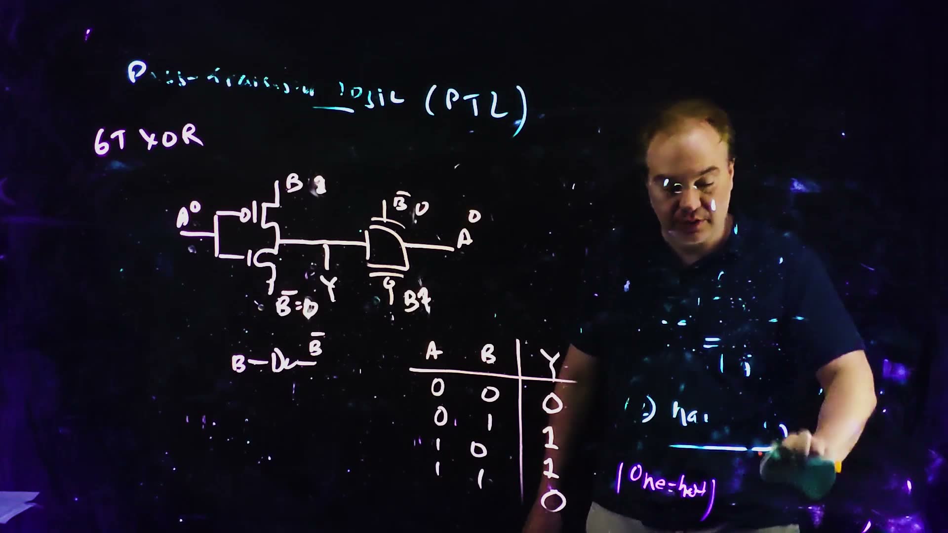
“If you ask any microprocessor designer what’s the six-transistor XOR, they’ll know exactly what you’re talking about. But it’s actually a very curious circuit. And it’s actually not a static CMOS circuit, which most people actually don’t realize” (41:20).
The circuit and its truth table
board (42:02; the device names M1–M6 are MT21-3’s, added here):
- a PFET with gate A (M3) connects B to Y, and an NFET with gate A (M4) connects to Y: an “inverter” of A whose supplies are B and ;
- an NFET with gate (M5) and a PFET with gate B (M6), in parallel, connect A to Y: a complementary pass pair;
- an inverter (M1, M2) makes from B. Only four transistors are visible; the inverter makes six (42:27).
Its truth table (board, 42:53–44:25)
- A = 0, B = 0: , the pass pair is on and passes A = 0. Y = 0.
- A = 0, B = 1: the pass pair is off; the A = 0 “inverter” connects Y to B = 1 through M3. Y = 1.
- A = 1, B = 0: the pass pair passes A = 1. Y = 1 (M4 also connects Y to , consistent).
- A = 1, B = 1: the pass pair is off; M4 connects Y to . Y = 0.
- Y is 1 when A and B differ: XOR.
The tool that disagreed
At IBM, a colleague’s Boolean equivalence checking tool traced the logic through the transistors of every circuit and compared it with the VHDL (44:35). It flagged this circuit: “My god, there’s a collision here. This is actually a ratioed logic circuit” (45:07). “I said, that’s ridiculous, your tool is broken … and sure enough it is” (45:34).
The failing transition
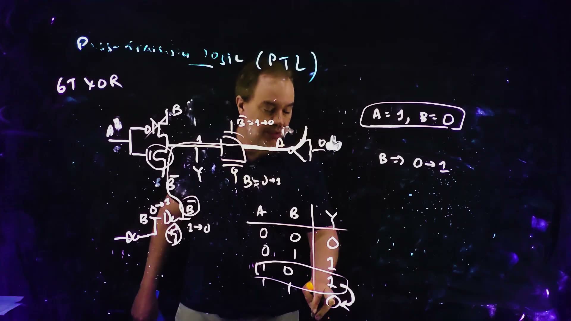
To see it, put in the gates that drive A and B, “so every node here is driven” (46:05).
The fight (board, 46:33–50:43)
- Start at A = 1, B = 0 board. , the pass pair is on, and Y is pulled up to 1 through it from the PFET of A’s driver. M4 (gate A = 1) is on too, joining Y to , which is also 1. Everything is consistent.
- Now switch B from 0 to 1 board. Y should go from 1 to 0: should fall, turn off the pass NFET M5, and let M4 pull Y down to .
- is pulled down by M2, the NFET of the B inverter.
- But is still connected upward: from , through the PFET of A’s driver, through the pass NFET M5 (its gate is , still 1), to Y, then through M4 (gate A = 1), to (49:07) board.
- That path is a three-high stack, and it pulls up through NFETs, which are weak at that. But if it were sized very large and M2 were “really, really wimpy”, M2 could not pull to 0 (50:15).
- Then stays high, M5 stays on, and Y stays at 1: the wrong answer for A = B = 1 (50:43).
The test for ratioed logic
The failing sizing is “very unlikely … that’s just not going to happen in practice”, but it exists: the lecturer sized the gate that way himself and “this gate would no longer function correctly” (51:13–52:09). “This six-transistor XOR gate, even though it’s extremely convenient and compact, is actually a ratioed logic circuit” (52:09).
Replay it in the widget of Section 4: choose “6T XOR”, start at A = 1, B = 0, and set B = 1. (The readout’s “test” line replays this transition for whatever sizes the sliders set.) With the default sizes, the “on the way here” line shows a fight at (1.25 V) that M2 wins. Now set M2 to 0.2 µm, go back to B = 0, and set B = 1 again.
What to notice.
- With M2 = 0.2 µm, stays at 3.1 V and Y at 3.75 V, a 1, for A = B = 1. The gate is stuck in the wrong state, with current flowing from to ground.
- With sensible sizes, every row of the truth table comes out right, and tracing the switches row by row, as the lecture does at 42:53, gives XOR whatever the sizes. A truth table can’t show a ratioed failure; only a transition does. (With M2 = 0.2 µm the widget’s row 11 fails too: starting from 0 V everywhere, first charges high through M1 before B arrives, and the same fight follows.)
- added 00 → 01 also has a brief fight (at Y), but it ends however the gate is sized, because falls on its own. Transient overlap is not what makes a gate ratioed; a fight whose winner decides the answer is.
Worked example. added The widget’s estimate of the fight, with every on-device as a resistor (Chapter 7’s model; a PFET counts ). A’s driver PFET is 2 µm wide, M5 and M4 are 1 µm.
- The path from to : A’s driver PFET (), M5 (), M4 (): in series.
- M2 of width pulls down with .
- Divider: .
- : , read as 0. The gate switches.
- : , read as 1. M5 stays on; Y sits at 3.75 V, read as 1. The gate fails.
- The switch-over is where , so : M2 must be weaker than the three-device path. Pulling up through two NFETs is weaker than this model says, so a real failure needs an even weaker M2.
Check yourself In the 6T XOR with drivers, the input moves from A = 1, B = 0 to A = 1, B = 1. Name the two paths that fight, the node where they fight, and the single device whose weakness lets the wrong one win.
The node is . Pulling down: M2, the NFET of the inverter that makes . Pulling up: through the PFET of A’s driver, the pass NFET M5 (gate , still 1), Y, and M4 (gate A = 1). If M2 is weak enough, stays high, M5 stays on and Y stays 1. (MT21-3 asks how one could size the circuit to fail.)
Check yourself Your friend says: “The 6T XOR is static. I checked all four rows of the truth table and each has exactly one path from Y to a rail.” What is wrong with the argument?
Each settled state is fine, but the test of static CMOS is that it works for any sizing. On the transition from 10 to 11 two paths fight at (and through it at Y), and because feeds back to the gate of M5, the loser of that fight decides the final state. With a weak enough M2 the gate settles in the wrong state, so its correct operation depends on sizing: ratioed.
10. Ratioed logic and pseudo-NMOS
The idea. In ratioed logic the output is connected to both rails at once in some state, and the stronger side wins. Pseudo-NMOS does this on purpose: an always-on PFET load against NFETs. Its low is not ground, it draws static power, but it makes very wide NOR gates cheap.

Where it comes from: NMOS logic
Before CMOS, chips could not mix NFETs and PFETs, so logic was NMOS only; the first major VLSI textbook, Mead and Conway’s, uses NMOS logic (53:26). It had two kinds of NFET (54:02) board:
- enhancement mode, the kind we use: a positive threshold, so a gate bias is needed to form a channel;
- depletion mode, drawn with a thick channel: a negative threshold, so it is on at , and a gate bias is needed to turn it off (54:34–54:49).
With , a depletion device is always on, “kind of almost like a resistor load” (54:57) board. It was the pull-up network, over enhancement NFETs as the pull-down (55:11):
- all inputs 0: the depletion load pulls the output to ;
- any input 1: that NFET overpowers the load and pulls the output down, but not to ground: where it settles depends on the relative strength of the NFET and the load (55:39).
Ratioed logic’s two problems
board (56:06):
- Non-rail logic lows: the low output is not at ground.
- Static power: while the output is low, current flows from through the load and the NFET to ground, all the time, not only while switching (56:32).
Pseudo-NMOS
CMOS designers wanted to keep the structure, so they used a PFET with its gate tied to ground as the always-on load (56:59) board: “pseudo-NMOS, because it’s like NMOS, except it’s using a PFET”. It has exactly the same two problems (57:33).
Its advantage: a wide NOR, with many NFETs in parallel. In complementary static CMOS an -input NOR needs a series stack of PFETs, slow especially for the devices far from the output (Chapter 7’s stack limit). Pseudo-NMOS needs one PFET, whatever (57:33–58:07). One such use is in PLAs, arrayed logic that comes later in the course (58:40).
What to notice.
- With the load at a quarter of one NFET’s strength, and the gate burns about 3 mW whenever its output is low, against the CMOS inverter’s zero.
- Turn on more NFETs: drops, but the current hardly changes. The saturated load sets it.
- Make the load as strong as an NFET: the “low” rises to 2.5 V, above the next gate’s . The ratio must be designed.
- The high is a full , with no current.
Deriving the low level by current balance (added; Chapter 6's method)
- The load’s always; with the output low, it is saturated: .
- One NFET with its gate at is in triode: .
- Set and write : .
- Take the smaller root: .
- With , , : . (The widget’s 0.64 V includes the output slope λ.)
Common mistakes.
- Expecting a ratioed gate’s low to be 0 V. It is set by the strength ratio.
- Forgetting the static power. It flows for as long as the output is low; in a chip with many such gates it dominates (Lecture 11 adds how it gets in the way of testing, Chapter 11).
Check yourself A pseudo-NMOS gate has VDD = 5 V, VT = 1 V for both devices, and a load PFET with a quarter of one NFET's β. Using flat saturation, find VOL with one input high and with two inputs high, and the static current with βn = 0.25 mA/V².
One input: . Two inputs act as one NFET of twice the β, so : . The current is set by the saturated load: , in both cases, from 5 V.
Check yourself You need an eight-input NOR. How many transistors does complementary static CMOS need, and how tall is its tallest stack? And pseudo-NMOS?
Complementary: 8 NFETs in parallel and 8 PFETs in series, 16 transistors, with an eight-high PFET stack, far beyond the limit of two or three. Pseudo-NMOS: 8 NFETs and one load PFET, 9 transistors, no stack at all, at the price of a non-rail low and static power.
Formulas to remember
| Formula | Meaning |
|---|---|
| one gate order that is an Euler path of both networks | shared diffusions, unbroken rows, straight polys |
| contact a diffusion if its net leaves the row or recurs | uncontacted shared diffusion = series internal node |
| b bordered, a abutted, s shared | layout-dependent letters, source then drain |
| – → fingers, each ≤ 10–15 µm | aspect ratio and the gate’s RC delay |
| exactly one path to or ground in every allowed state | static; outside complementary CMOS it depends on the inputs |
| NFET passes and ; PFET passes and | degraded levels; drops add only through a gate |
| NFET ∥ PFET on complementary gates | complementary pass transistors: full rail, more area |
| inverter + weak PFET feedback | half latch: full high, slower fall, ratioed |
| selects one-hot | pass-transistor multiplexer static |
| delay of a CCC, driving gate included | never drive a pass transistor from an ideal source |
| static works at any sizing; ratioed depends on sizing | the 6T XOR is ratioed |
| , | pseudo-NMOS (added): non-rail low, static power |
The lecture’s boards