FS2. Final practice: clock generation, pulsed flip-flops and storage cells
This page practises the three kinds of clocking and storage question the past finals ask outside plain latch timing (which is the companion page FS1’s, “flip-flop and latch timing”). Clock generation: a few gates and delay blocks make the clocks a latch needs, and you sketch what comes out (FN12-7a). Pulsed flip-flops: a clock chopper turns each clock edge into a short pulse, the pulse’s width is capped by hold, and a pulse that is too short for its driver arrives as a runt (FN19-5). Storage-cell design: why a latch cannot be written and how to fix it (FN19-9), and a small sequential design with a synchronous reset (Problem Set 5’s counter, PS5-Q2). Together they are 47 points of the two finals (FN12-7a 15, FN19-5 22, FN19-9 10).
Each family opens with How to approach it: the picture that announces it, the moves in order, the formulas with their conditions, and the traps. Then each question is quoted in the paper’s own words and solved part by part: what it asks, the idea, why this formula, the steps (each with its reason first), a check by another route, the answer, and what to remember. Try each part first; open the Hint if stuck. The key’s verdict is folded at the end of each part: FN12 has a key, FN19 has none (only an unofficial proposed solution, used as a cross-check), and PS5 has none. Every family ends with harder variations added, longer chains on unfamiliar circuits with more arithmetic, the way the real Fall 2026 midterm was harder than the samples. Page numbers are the PDF’s physical pages.
Before you start. These questions rest on Chapter 13 (the static latch, the write fight, gated feedback, the master–slave flip-flop), Chapter 14 (two-phase clocks and their generator, pulsed latches, the chopper, runt pulses) and Chapter 15 (TSPC and half latches). Each question below restates what it uses.
Symbols
| Symbol | Meaning | Unit | First appears |
|---|---|---|---|
| φ, φ̄ | a global clock and its complement (made by an inverter) | — | FN12-7 |
| φ1, φ2 | the two phases a local generator makes from φ | — | FN12-7 |
| , | the delay blocks of the generator: φ2 delayed by feeds φ1’s NOR, φ1 delayed by feeds φ2’s NOR | ps | FN12-7 |
| Chapter 14’s name for the non-overlap window, when both phases are low | ps | FN12-7 | |
| , | the delay of one NOR gate, of one inverter | ps | Variation 1 |
| ψ1, ψ2 | the phases of the NAND generator (Variation 2) | — | Variation 2 |
| the chopper’s delay block, which the paper calls the pulse width | ps | FN19-5 | |
| CLK1, CLK2; lclk | the clocks at the two latches of FN19-5; a chopped (pulsed) local clock | — | FN19-5 |
| the width of a chopped pulse | ps | FN19-5 | |
| signed skew: the capturing clock’s edge minus the launching clock’s edge (: the capture clock is early) | ps | FN19-5 | |
| , , | clock-to-Q delay, setup time, hold time of a latch or flip-flop | ps | FN19-5 |
| the delay of the logic between two clocked elements (its shortest value for hold) | ps | FN19-5 | |
| FO1 delay: an inverter driving one copy of itself (the paper’s symbol; the chapters write ) | ps | FN19-5 | |
| , , | gate capacitance per µm; a driver’s input capacitance; its load | fF/µm, fF | FN19-5 |
| a driver’s 50% delay into its load | ps | FN19-5 | |
| the time constant of an RC whose 50% delay is : | ps | FN19-5 | |
| , , | supply; an inverter’s switching threshold; a threshold voltage | V | FN19-5, FN19-9 |
| A, X, Y | FN19-9’s input, its storage node (named here), its output | — | FN19-9 |
| , | the course’s device resistance (a 1 µm NFET pulling down) and a width; an NFET of width is , a PFET | kΩ·µm, µm | FN19-9 |
| , | the series resistance of the devices pulling X down, pulling it up | — | FN19-9 |
| clk, | a latch’s clock and its complement | — | FN19-9 |
| , ; reset | the counter’s two bits; its synchronous reset input (the paper’s name) | — | PS5-Q2 |
| , | the clock period and frequency | ps, GHz | PS5-Q2 |
| , , | a dynamic node’s capacitance, its leakage current, the droop the next gate still reads correctly | fF, nA, V | Variation 5 |
How to approach a clock-generation question
Recognize it by the picture: a box labelled CG (or CC) followed by “≡” and a handful of gates, an inverter and one or two boxes marked Δ, with one clock in and one or two clocks out. The prompt says “sketch the waveforms”, “indicate the delays on your sketch”, or “how must Δ be adjusted”. FN12-7 is the type: two NOR gates cross-coupled through delay blocks make two phases that are never high together.
The moves.
- Read every wire. Write each gate’s output as a function of its inputs, with each delayed input written as the signal it comes from, shifted: . Which net feeds which delay block is the whole question.
- Find each gate’s controlling value. A NOR’s output is 0 as soon as any input is 1 (1 controls a NOR); it goes to 1 only when all inputs are 0. A NAND is the mirror: 0 controls it.
- Walk each edge of the input clock. When an input takes the controlling value, the output changes at once (plus the gate’s own delay, if it counts). When an input leaves the controlling value, the output must wait for its slowest other input, usually a delayed signal: that wait is where the Δ appears on the sketch.
- Mark the windows between the edges that the delays separate, and say which edge each window follows.
- If a timing question follows, decide which phase drives the master latch and which the slave: the window between the master’s closing edge and the slave’s opening edge is the one that protects hold.
The formulas.
- The generator’s windows (Derive, from the NOR truth table; Chapter 14 §3): for , with ideal gates, φ2 rises after φ rises and φ1 rises after φ falls; each phase falls at once with its own input. It holds while each delay is shorter than the half period it sits in.
- With gate delays (Derive, Variation 1): each window becomes , because the delayed signal is itself a NOR output, one gate delay late.
- The window hold needs (Derive, Chapter 14 §3): , paid for on the long path, .
Decide on the way: whether gate delays are ignored (FN12-7a says so), which phase is the master, and whether the question wants the phases apart (non-overlap, for latches) or together (overlap, for two-phase domino; Variation 2).
Traps. Swapping and : read which output each delay block takes. Drawing the two phases as mirror images: the windows are at one edge and at the other, and with gate delays the phases have different widths. Forgetting that a phase falls at once: only the rising edges wait.
1. FN12-7: a local clock generator (15 points of 30)
You need
The NOR gate. A NOR’s output is high only when both inputs are low. If either input is 1, the output is 0, whatever the other input does: 1 is the NOR’s controlling value.
A delay block. A box Δ (an even number of inverters, so it does not invert) passes its input through unchanged, later: its output at time is its input at .
Why two non-overlapping phases (Chapter 14 §3). A flip-flop is two latches on two phases, the master on φ1 and the slave on φ2. If φ1 falls a little before φ2 rises, both phases are low for a moment, the non-overlap window: the receiving master closes before the launching slave opens, which protects hold, at the cost of that much dead time on the long path. A local generator makes the window from one global clock wire.
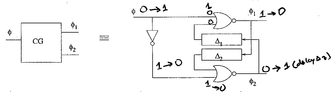
The question (FN12-7, p10, in the paper’s words). Consider the “local clock generator” circuit shown below, used to generate two clock phases locally from a single-wire global clock. The delay blocks (labelled with and ) could be implemented with an even number of inverters (for example).
FN12-7’s local clock generator (p10, redrawn): CG ≡ two NORs and an inverter. and : each delay block takes the other phase. Below, the paper’s φ (50% duty, printed from half a period before its first rising edge to three periods), with empty rows for φ1 and φ2. The key’s handwritten notes are left out.
The exam’s own figure (FN12-7, p10)
Part (a): sketch φ1 and φ2 (15 points)
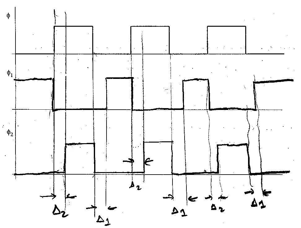
FN12-7a, p10. Sketch the and waveforms for the waveform shown below. Ignore the gate delays of the inverter and NOR gates but indicate the and delays on your sketch. (15 points)
Hint
What it asks. Two waveforms, drawn under the paper’s φ (a square wave, low first, with three high pulses): φ1 and φ2, with the two delays marked where they show. The word that sets the method is “ignore the gate delays”: every gate switches the instant its inputs allow, so the only times on the sketch are φ’s edges and those edges shifted by or . Nothing is computed; the 15 points are for getting each edge in the right place, with its reason.
The idea. Write each output as a Boolean function of its inputs, then walk the edges of φ one at a time. A NOR answers a 1 on any input at once, so each phase falls the instant its direct input (φ for φ1, φ̄ for φ2) goes high. It rises only when both inputs are low, and one of them is the other phase delayed. So a phase can rise only a delay after the other phase has fallen. That is what keeps them apart: there is always a gap in which both are low.
Why this formula. The two equations are read straight off the wires. The upper NOR takes φ directly and the output of , whose input is the φ2 line, so . The lower NOR takes φ̄ from the inverter and the output of , whose input is the φ1 line, so . A delay block’s output at time is its input at : it is an even chain of inverters, so it does not invert, as the paper says. The NOR rule is all that is needed: output 1 exactly when both inputs are 0. Two conditions make the walk below valid. First, the gate delays are zero (the paper’s instruction); Variation 1 shows that with real gates each gap grows by one NOR delay. Second, each delay is shorter than the half period it falls in: shorter than φ’s high time, shorter than its low time, or the delayed phase would rise after φ had already changed again. The tempting shortcut, “φ1 is φ̄ and φ2 is φ, each delayed”, is wrong: a delayed copy would also be late at its falling edge, and that is the edge that does not wait here.
FN12-7a, edge by edge
- Start before the first edge, with φ low. Because φ̄ = 1 is an input of φ2’s NOR, φ2 = 0. Then and φ = 0, so both inputs of φ1’s NOR are low: φ1 = 1. The circuit sits in a steady state with φ1 high and φ2 low.
- φ rises. Because φ is a direct input of φ1’s NOR, φ1 falls at once. At the same instant φ̄ falls, so φ2’s NOR has one low input; but its other input is φ1 delayed by , and that copy still shows the old 1 for . So φ2 rises after φ rises. For those both phases are low: the first window.
- φ stays high. φ1 is held low by φ; φ2 stays high because φ̄ = 0 and the delayed φ1 is now 0.
- φ falls. φ̄ rises, and it is a direct input of φ2’s NOR, so φ2 falls at once. φ1’s NOR now sees φ = 0, but its other input is φ2 delayed by , still 1 for . So φ1 rises after φ falls. For those both phases are low: the second window.
- φ stays low, φ1 stays high, φ2 stays low, and the next rising edge of φ repeats step 2. Every cycle looks the same.
- Draw it. Under each high pulse of φ: φ1 low for the whole pulse, and φ2 high from after the rising edge to the falling edge. Under each low stretch of φ: φ2 low, and φ1 high from after the falling edge until the next rising edge. Mark as the gap after each rising edge of φ and as the gap after each falling edge.
Check. Two independent tests. First, the never-both-high property: at every moment one of the two NORs has a 1 on its direct input (φ for the top one, φ̄ for the bottom one), so at most one phase can be high, and the sketch must never show both high; it doesn’t. Second, a limit: let both delays shrink to zero. The equations then give φ1 = NOR(φ, φ2) and φ2 = NOR(φ̄, φ1), whose steady states are φ1 = φ̄ and φ2 = φ, a plain complementary pair; the sketch, with its gaps shrunk to nothing, must turn into exactly that, and it does. A third, mechanical check: this page’s test runs the same circuit in an event-driven gate simulator, and the edges come out at after φ rises and after φ falls.
Answer: φ2 is high from after each rising edge of φ until that pulse’s falling edge; φ1 is high from after each falling edge of φ until the next rising edge. Each phase falls with an edge of φ at once; both are low for after every rising edge and for after every falling edge.
Remember. A NOR falls at once and rises late. In a cross-coupled generator, each phase waits a delay for the other one to be gone: read which phase feeds which delay, then walk the edges.
The answer key agrees
The key’s sketch (FN12-7a, p10)
Variations: clock generation
Two added variations added, each a chain of dependent parts. Variation 1 puts the gate delays back into FN12-7’s generator and asks for a window, a hold repair, its cost and the fastest clock. Variation 2 swaps the NORs for NANDs: the phases then overlap, which is what two-phase domino wants and what a pair of latches must never see.
Variation 1: the generator with its gate delays (added)
Variation 1: the generator with its gate delays
The question added. FN12-7’s generator is built from real gates: each NOR takes ps and the inverter ps; ps and ps. φ runs at 1 GHz with a 50% duty cycle and rises at . The phases clock master–slave flip-flops, master on φ1 and slave on φ2, with ps, ps and ps. (a) Find every edge of φ̄, φ1 and φ2 in the first cycle. (b) Give the two non-overlap windows, in numbers and in terms of and , and the two phases’ high times. (c) A receiving pair of flip-flops gets its phases 150 ps late, and the shortest logic between the pairs is none at all (a shift register). Does hold pass? If not, what repairs it? (d) With that , what is the longest logic allowed between two pairs on unskewed clocks at ns, and between the late pair? (e) Each latch needs its clock high for at least 200 ps to be written reliably. With the of (c), what is the shortest period of φ?
Hint
What it asks. The same circuit as FN12-7a with the gates no longer instantaneous, and then four consequences in a chain: the size of the windows, whether one of them is wide enough for a skewed shift register, what the repair costs the long path, and how fast φ may run before a phase gets too short. The word that decides the method is “edges”: every answer comes from a list of edge times, so build that list first, carefully, and read everything else off it.
The idea. The walk is the one of FN12-7a with each gate adding its delay to whatever passes through it. An edge of φ reaches each NOR by two routes, directly (or through the inverter) and the long way round, through the other NOR and a delay block. A NOR that falls does so one gate delay after a 1 arrives; a NOR that rises waits for its last input to fall. The window between the two phases is then the long route’s extra length: one delay block and one NOR. The hold and long-path questions are Chapter 14’s, with this window as .
Why this formula. Four relations, each with its reason.
- Edge times. A gate’s output changes after the input change that decides it. For a NOR, a rising input decides at once (1 controls); a falling input decides only if it was the last one high. So φ1 falls at after φ rises, but φ2 rises at after φ rises: its two inputs are φ̄ (low after ) and the delayed φ1 (low after ). Here , so the delayed φ1 is last.
- The windows. From φ1’s fall at to φ2’s rise at is : one block and the NOR that responds to it. The inverter drops out of the window, as long as it is faster than that route; it only shifts both edges at φ’s falling edge by .
- The hold window (Chapter 14 §3): with the master on φ1 and the slave on φ2, data launches when φ2 rises (the slave opens), and the receiving master closes when its φ1 falls, late. The window moves that capture edge earlier relative to the launch: . The window that counts is the one from φ1’s fall to φ2’s rise, the master’s closing to the slave’s opening; widening the other one does nothing for this race.
- The long path: , Chapter 14’s board form without skew; a late capture clock adds its skew back.
Variation 1
- (a) φ rises at 0. Because the inverter takes 20 ps, φ̄ falls at 20. Because φ is a direct input of φ1’s NOR and a 1 controls a NOR, φ1 falls one NOR delay later, at 30.
- (a) φ2 rises. Its NOR needs both inputs low. φ̄ is low from 20; the delayed φ1 falls after φ1, at , which is later. So φ2 rises one NOR delay after 90: at 120.
- (a) φ falls at 500. φ̄ rises at 520, and a 1 controls φ2’s NOR, so φ2 falls at 550. φ1’s NOR has φ low from 500 and the delayed φ2 low from ; the later one decides, so φ1 rises at 680. At the next rising edge, 1000, φ1 falls at 1030, and the cycle repeats.
- (b) The windows. From φ1’s fall (30) to φ2’s rise (120): 90 ps . From φ2’s fall (550) to φ1’s rise (680): 130 ps .
- (b) The high times. φ2: 430 ps . φ1: 350 ps . The phases are unequal: φ1 loses its delay block, and the inverter shifts time from φ1 to φ2.
- (c) What hold needs. Because the window must cover the skew and the hold time that the flip-flop’s own delay does not: ps. The window after the master’s closing edge is 90 ps: hold fails by 35 ps.
- (c) The repair. Because that window is , widen : , so 95 ps. ( would not help: it sits after the slave’s closing edge.)
- (d) The cost. Because the window is dead time in every cycle, the long path between unskewed pairs loses it: 815 ps, against 940 ps with no window. Between the pair whose capture clock is 150 ps late, the late edge gives the time back: 965 ps.
- (e) The shortest period. With : φ1 is high for , which must be at least 200, so ps; φ2 is high for , so ps. The narrower phase, φ1, sets it: 700 ps, about 1.43 GHz, where φ1 is high for 200 ps and φ2 for 245 ps.
Variation 1’s edges added, computed from ps, ps, ps, ps, φ at 1 GHz: each window is a delay block plus one NOR, 90 ps long after φ rises (30 to 120 ps) and 130 ps long after it falls (550 to 680 ps).
Check. Every instant of a period belongs to exactly one of four intervals: φ1 high, φ2 high, or one of the two windows (one NOR always has a 1 on its direct input, so the phases are never both high). A paper route for (c), walked on the timeline with ps: the launching slave opens when φ2 rises, at ps, and the data reaches the late master ps later, at 195 ps. That master closes when its φ1 falls, ps, and needs its input held until ps: met exactly, as (c) says ✓. Independently, this page’s test runs the circuit in an event-driven gate simulator with these delays and finds the same six edges (20, 30, 120, 520, 550, 680 ps), and a 125 ps window after the change of .
Answer: (a) φ̄ falls at 20 and rises at 520 ps; φ1 falls at 30 and rises at 680 ps; φ2 rises at 120 and falls at 550 ps. (b) Windows 90 ps () and 130 ps (); φ2 high 430 ps, φ1 high 350 ps. (c) Hold needs 125 ps and fails by 35 ps; ps. (d) 815 ps between unskewed pairs, 965 ps into the late pair. (e) ps.
Remember. With real gates each window is the delay block plus one NOR, and the two phases come out unequal. For hold, widen the window that follows the master’s closing edge, then pay for it on the long path and check that the shorter phase is still long enough.
Variation 2: a NAND generator, whose phases overlap (added)
Variation 2: a NAND generator, whose phases overlap
The question added. Replace both NOR gates of FN12-7’s generator by NAND gates, keeping every wire: and . Gates are ideal; φ has ns, 50% duty, rising at 0; ps, ps. (a) Sketch ψ1 and ψ2. (b) When are both high, and for how long? (c) The phases clock a two-phase domino pipeline, a block evaluating while ψ2 is high feeding a block evaluating while ψ1 is high, and the designer wants to drop the mid-cycle latch between them. The ψ1 block’s first stage takes 40 ps to evaluate, and 10 ps of margin is wanted. Is enough? How long does the ψ2 block have to evaluate, and to precharge? (d) Someone instead clocks static master–slave flip-flops with these phases, master on ψ1 and slave on ψ2, ps and ps. What shortest logic does hold now demand, with no skew and with the receiving pair 60 ps late? (e) Which generator belongs with which design?
Hint
What it asks. An unfamiliar circuit, read the same way as FN12-7, then two uses of its result: in a domino pipeline, where Chapter 15 wants the phases to overlap, and in a flip-flop, where Chapter 14 wants them apart. The words that decide the method are “both high”: with NANDs the danger and the benefit are overlaps, not gaps.
The idea. A NAND is a NOR turned inside out: 0 controls it, and its output is 1 as soon as any input is 0. So each phase now rises at once with its direct input and falls only a delay after the other phase has risen. Instead of two gaps per cycle, the generator makes two overlaps, one after each edge of φ, and long. Whether an overlap is wanted depends on what the phases clock.
Why this formula. The NAND rule: output 0 exactly when both inputs are 1. The edge walk is FN12-7a’s with the roles of 0 and 1 swapped. For the domino use, Chapter 15’s rule for dropping a mid-cycle latch is (Chapter 15 §10): the block that receives must start evaluating (its clock rises) before the block that sends starts precharging (its clock falls), for long enough that its first stage has discharged, because domino is monotonic and a discharged node stays down when its input goes away. For the flip-flop use, an overlap is a non-overlap window of negative length: in Chapter 14’s hold inequality the window enters with the opposite sign, , where is the time from the launching slave’s opening to the receiving master’s closing. While both latches are open the data can run straight through the pair, and the race gets that much longer.
Variation 2
- (a) Before the first edge, φ low. Because φ = 0 is a direct input of ψ1’s NAND, ψ1 = 1. φ̄ = 1 and the delayed ψ1 = 1, so ψ2 = 0.
- (a) φ rises at 0. φ̄ falls, and a 0 controls ψ2’s NAND: ψ2 rises at once. ψ1’s NAND now has φ = 1, but the delayed ψ2 still shows 0 until , so ψ1 falls at 30 ps.
- (a) φ falls at 500. A 0 on ψ1’s direct input: ψ1 rises at once, at 500. ψ2’s NAND has φ̄ = 1, and the delayed ψ1 still shows 0 until 550, so ψ2 falls at 550 ps.
- (b) The overlaps. Both are high on , 30 ps after φ rises, and on , 50 ps after φ falls; the next cycle repeats them from . ψ2 is high for 550 ps and ψ1 for 530 ps.
- (c) The mid-cycle latch. The sending block is on ψ2, the receiving one on ψ1. ψ1 rises at 500 and ψ2 falls at 550, so ps. Because the receiving block’s first stage must evaluate while its input is still valid, it needs ps: just enough.
- (c) The budgets. The ψ2 block starts evaluating at 0 and its result must be ready when ψ1 rises at 500: 500 ps, the full half cycle, because this generator stretches ψ2 instead of moving ψ1’s edge earlier (in Chapter 15’s example the overlap came out of the sending block’s budget). The price is its precharge: ψ2 is low only from 550 to 1000, 450 ps.
- (d) The flip-flop race. Data launches when the slave opens, ψ2 rising at 0. The receiving master closes when ψ1 falls, at 30 ps. So ps, and hold demands 5 ps with no skew, and 65 ps with the receiving pair 60 ps late. A shift register, with no logic, now fails even on perfect clocks.
- (e) The match. The NOR generator keeps the phases apart: latches and flip-flops, whose hold it protects. The NAND generator makes them overlap: two-phase domino that drops its mid-cycle latches. Each delay block sets the length of the gap, or of the overlap, after one edge.
Variation 2’s NAND generator added: FN12-7’s wiring with NAND gates, and its phases computed for ns, ps, ps, ideal gates. Each phase rises with an edge of φ and falls a delay after the other has risen, so both are high (shaded) for after each rising edge of φ (0–30 and 1000–1030 ps) and for after each falling edge (500–550 ps).
Check. At every instant one of the two NANDs has a 0 on its direct input (φ for ψ1, φ̄ for ψ2), so at least one phase is high, always. A second route, by De Morgan: , so and : FN12-7’s NOR generator, with as its φ1, as its φ2, and the two delays swapped. By FN12-7a, its φ2 rises ps after φ rises and its φ1 rises ps after φ falls: so ψ1 falls at 30 ps and ψ2 at 550 ps, and the NOR generator’s gaps are this one’s overlaps ✓. This page’s test also simulates the NAND circuit and finds ψ2 rising at 0 and falling at 550 ps, ψ1 falling at 30 and rising at 500 ps.
Answer: (a) ψ2 high from each rising edge of φ to 50 ps after the falling edge; ψ1 high from each falling edge to 30 ps after the next rising edge. (b) Both high for 30 ps after φ rises and 50 ps after φ falls. (c) Yes, exactly: 50 ps ≥ 40 + 10 ps; the ψ2 block keeps 500 ps to evaluate and has 450 ps to precharge. (d) ps without skew, 65 ps with the pair 60 ps late. (e) NOR generator for latches and flip-flops, NAND generator for two-phase domino.
Remember. Cross-coupled NORs make gaps (both low), cross-coupled NANDs make overlaps (both high), each as long as a delay block. Latches want gaps; domino that drops a latch wants an overlap.
How to approach a pulsed-latch question
Recognize it by a box CC (clock chopper, one-shot) that expands to an inverter, a delay block Δ and a NOR, feeding the clock input of a latch; by the phrases “clock-chopped flip-flops”, “the pulse width of the chopped clock”, “a hold time on the closed clock edge”; and, in a second part, by a driver with a load capacitance and the question “what will be the height of the pulse?”. FN19-5 is the type.
The moves.
- Read the chopper. Find when both NOR inputs are low: for a NOR of the clock and a delayed, inverted copy, that is just after each falling clock edge, for as long as the delayed copy lags (Chapter 14 §5). The width is the chain’s delay; the papers call Δ the width and ignore the single inverter.
- Put the launching pulse’s opening at and the receiving pulse’s opening at , the signed skew: negative if the receiving clock arrives earlier.
- Hold. The pulsed latch is transparent until its pulse closes, so the earliest new data, , must arrive after . Solve for the widest pulse.
- The long path, if a period is given: the receiving latch takes data until its pulse closes, so one stage’s deadline moves later; but data that arrives inside the pulse leaves late by the same amount, so that time is borrowed from the next stage (Chapter 14 §4). For a pipeline of equal stages, use the limit that borrows nothing: the data reaches the receiving latch by its pulse’s opening.
- Distribution. The pulse leaves through a driver whose delay into its load is . If the pulse does not reach half the swing: a runt. Its height is of .
The formulas.
- Pulsed hold (Memorize, Chapter 14 §4): , so . It holds at the fast corner, with the shortest logic.
- A driver’s delay (Memorize, Chapters 7–8): , its own drain capacitance ignored; the delay is the 50% point of the output’s swing.
- Runt height (Derive, Chapter 14 §6): an RC driven by a step reaches of its swing; the 50% point at gives ; so after the output has moved of .
Decide on the way: the sign of the skew (an early receiving clock helps hold and allows a wider pulse); whether is given (FN19-5 gives none: take it as zero and say so); and the runt convention (this guide uses Chapter 7’s 50%-point delay; say so on the paper).
Traps. Treating an early receiving clock as late, which caps the pulse 200 ps too low in FN19-5. Measuring hold from the pulse’s opening instead of its closing. Drawing the chopper’s pulse at the rising edge. Using itself as the time constant without saying so. Curing a runt by widening the pulse: hold caps the width.
2. FN19-5: a clock chopper and a runt pulse (22 points)
You need
The NOR clock chopper (Chapter 14 §5). A NOR of a clock and a copy of it delayed through an odd number of inverters gives one short high pulse per cycle, just after each falling clock edge: only then are both inputs low, the clock already low and the inverted copy not yet risen. The pulse is as wide as the chain’s delay; it does not depend on the clock’s period or duty cycle.
A pulsed latch (Chapter 14 §4). One latch clocked by the short pulse acts almost like a flip-flop: it is transparent only while the pulse is high, and its setup and hold times are measured at the pulse’s closing edge.
A driver’s delay (Chapter 7’s model). An inverter whose FO1 delay is takes to drive a load , where is its own input capacitance; this delay is measured at the 50% point of the swing.
The question (FN19-5, p11, in the paper’s words). Consider the clock chopper circuit shown below. The delay block (labelled ) can be implemented with an even number of inverters.
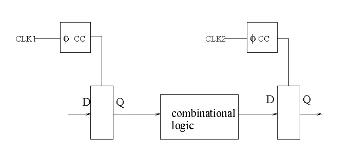
FN19-5’s figures (p11, redrawn). (a) The clock chopper: CC ≡ a NOR of φ and φ inverted and delayed by Δ, . (b) Two clock-chopped latches: each is clocked by its own chopper, from CLK1 and CLK2, with combinational logic between them.
The exam’s own figures (FN19-5, p11)

Part (a): the widest pulse (10 points)
FN19-5a, p11. Consider two clock-chopped flip-flops separated by combinational logic as shown below. Assuming that the combinational logic represents a fixed delay of 200 psec and there is skew between CLK1 and CLK2 such that CLK2 arrives 100 psec earlier than CLK1, what is the maximum value (the pulse width of the chopped clock) can have and still ensure correct functionality? Assume that the latches have a hold time of 50 psec on their closed clock edge. (10 points)
Hint
What it asks. The largest pulse width for which the second latch is not corrupted: a hold question, because only the maximum Δ is asked and the pulse width is the thing that makes pulsed latches race. The words that set the numbers: “200 psec” is the logic’s delay, and “fixed” means it is also the shortest; “CLK2 arrives 100 psec earlier” is the sign of the skew; “hold time of 50 psec on their closed clock edge” says hold is measured from the end of the pulse. No clock-to-Q delay is given, so take and say so.
The idea. A pulsed latch is open for the whole pulse. The second latch must take the old data, the value launched one cycle earlier, until its pulse closes and for 50 ps after. Meanwhile the first latch opens and lets the new data race toward it through 200 ps of logic. A wider pulse keeps the second latch open longer, so at some width the new data gets in before it closes: that width is the answer. The early CLK2 helps: the receiving pulse opens, and therefore closes, 100 ps sooner.
Why this formula. The constraint is Chapter 14’s pulsed short path, . Its left side is when the new data reaches the second latch’s D, measured from the first latch’s opening. Its right side is when the second latch stops caring about D: its pulse opens at , stays open for , and needs more. It applies because the two choppers are identical and pulse at the same edge of their clocks, so the pulses are offset by exactly the clocks’ skew; and because the logic is “fixed”, its shortest delay is 200 ps. The sign is the trap: with the capture clock early, ps, and the skew loosens the constraint. Adding it as if it were late gives 50 ps. Hold is measured from the closing edge because a latch that is still transparent is still listening; measuring from the opening edge would ignore the pulse width, the very thing the question asks about.
FN19-5a
- Read the chopper. . Because a NOR is high only when both inputs are low: just after φ falls, φ = 0, and the delayed φ̄ still shows the 0 it had while φ was high, for Δ. So each chopper pulses for Δ after each falling edge of its clock. (The inverter adds its own small delay to the width; the paper calls Δ the width, so it is ignored.)
- Place the pulses. Because both choppers pulse at the same edge, the pulses are offset by the clocks’ skew. Put the first latch’s pulse at . CLK2 is 100 ps early, so the second latch’s pulse runs from ps to .
- The new data. We need the earliest moment the second latch’s D can change. The first latch opens at 0 and, with no clock-to-Q delay given, its new output leaves at once; the logic takes 200 ps. So the new data reaches the second latch at 200 ps.
- What the old data must cover. The second latch is transparent until and needs D steady for 50 ps more: until .
- Solve. Because the new data must not arrive before that: , so 250 ps.
- Read the limit. At ps the second pulse closes at 150 ps, hold ends at 200 ps, and the new data arrives at exactly 200 ps: no margin left. A real design stays below.
FN19-5a at the limit added, computed from ps, ps, ps, CLK2 100 ps early and : the second latch’s pulse closes at 150 ps, its hold ends at 200 ps, and the new data reaches its D at exactly 200 ps.
Check. Two limits and a second constraint. Without skew, the second pulse would close at Δ and the bound would be ps: the 100 ps of early capture clock buys exactly 100 ps of pulse, the right sign and size. With CLK2 100 ps late, the bound would fall to 50 ps, which is why the sign matters. The long path, the other side of “correct functionality”, cannot bite here: data launched at 0 arrives at 200 ps, and the second latch’s next pulse closes at ps, so any period above 50 ps is fine.
Answer: ps (taking , which the paper does not give).
Remember. For a pulsed latch, hold is measured from the end of the receiving pulse: . An early receiving clock () allows a wider pulse.
The answer key agrees
Part (b): the chopped clock through a loaded inverter (12 points)
FN19-5b, p12. Assume that this chopped clock with the pulse width calculated in (a) is driven from an inverter with a load capacitance of 200 fF. The inverter is sized in a technology with a FO1 delay of . Assume a gate capacitance of . Sketch the waveform of the clock as received by the latch. What will be the “height” of the pulse? What problems might this present? (12 points)
Hint
What it asks. Three things about the 250 ps pulse of (a) once it passes through a clock driver: the shape of the waveform at the latch, how far it swings (its “height”, the paper’s quotation marks hinting that it will not be full), and what that means for the latch. The numbers that decide it are the driver’s size, µm, the load, 200 fF, and the FO1 delay, 25 ps: together they give the driver’s delay, which is compared with the pulse. “This chopped clock … is driven from an inverter” is read as the inverter being the clock net’s driver: its output is the chopped clock, a high pulse commanded for 250 ps, and the latch receives that pulse, rounded by the 200 fF.
The idea. A driver needs time to swing its load: its 50% delay . If the input pulse ends before the output has got that far, the output turns round halfway through its swing and never reaches the other rail. The pulse that arrives is a runt: shorter in height, and possibly too short to switch the latch’s clock at all. Here the pulse (250 ps) is shorter than the driver’s delay, so the runt is certain; the question is only how tall it is.
Why this formula. Two formulas, each with its conditions.
- The driver’s delay, . In the course’s model a stage’s delay is proportional to its load over its own input capacitance, and the FO1 delay is that ratio’s unit: an inverter driving a copy of itself has and takes (Chapter 7 §7). The inverter’s own drain capacitance is ignored (the paper gives none), and the 4/2 inverter is balanced in the course’s technology, where a PFET needs twice an NFET’s width for the same strength, so rising and falling take the same .
- The height, . Model the output as an RC driven by a step: it moves the fraction of its swing in a time . The course defines at the 50% point (Chapter 7 §1: the fitted already gives the 50% delay, so no extra 0.69), so and . Substituting, after the output has moved of , and then it turns back. The condition is a step input and an output starting from rest at a rail; the driver’s input switches cleanly at the pulse’s start and end, which fits. The tempting alternative is to use itself as the time constant: that counts twice and gives a taller runt (the KeyNote has the number).
FN19-5b
- The driver’s input capacitance. Because one input drives both devices: fF.
- Its load ratio. : it drives 16.7 copies of itself.
- Its delay into the load. Because each copy costs one FO1 delay: 416.7 ps, the time the output takes to swing halfway.
- Compare with the pulse. The pulse from (a) lasts 250 ps, : it ends before the output reaches the middle of its swing. A runt.
- The shape. Between pulses the chopped clock, the inverter’s output, sits at 0. When the pulse is commanded, the output rises along the RC curve, ; when the pulse ends, 250 ps later, it turns round and decays back toward 0 with the same time constant, ps (the driver is balanced). So the latch sees a low, rounded bump instead of a square pulse: a runt.
- The height. Because the output moves of the swing: 0.34. The clock rises only to , and has decayed to about by 1.5 ns. (If the chopped pulse were instead the inverter’s input, the latch would see the same depth as a dip from to , and the latch’s clock polarity would then be wrong as well.)
- The problems. The received clock never crosses , so the latch’s clock input may never switch: the latch never opens and the data is lost, what the lecture calls a pulse that “may not even turn the latch on” (Lecture13, 36:55). If it switches partly, the latch opens weakly and late, and its window depends on process, voltage, temperature and noise, so setup and hold are no longer controlled.
- The cure. The pulse cannot be widened: (a) caps it at 250 ps. So the driver must be faster: for ps, fF, a 10 µm inverter (6.67/3.33 µm), just to reach half the swing; for 90% of the swing, ps, so fF, 33.2 µm. Better still, put the chopper next to the latch it clocks (Chapter 14’s chopper in every flip-flop), so that the pulse never drives a large load.
FN19-5b’s chopped clock through the loaded inverter added, computed from ps and the 250 ps pulse, with the 50%-point RC model. Dashed: the chopped pulse. Solid: the clock the latch receives, which rises as for 250 ps, to , and then decays, to about by 1.5 ns. It never reaches .
Check. Chapter 14’s computed curves bracket the answer: a pulse of reaches 0.29 of the swing and one of reaches 0.5, so must lie between, and 0.34 does. A second route to the same number: , the fraction of the swing still left to go when the pulse ends. And the conclusion survives the other convention: with taken as the time constant, the height is , still short of half the swing.
Answer: The latch receives a rounded runt: the clock rises from 0 for 250 ps and decays with ps; its “height” is about , never , because the driver’s delay into 200 fF, 417 ps, is longer than the pulse. The latch may not open at all, or opens weakly and unpredictably; widening the pulse is not allowed by (a), so the driver must be about 10 µm or more, or the chopper local.
Remember. A pulse must be wider than the delay of whatever drives it, or it does not reach half the swing. Compute first; the height is .
The answer key differs
FN19 has no official key. The unofficial proposed solution has the same delay, 416.7 ps, but gives as its main height, using itself as the RC time constant; its alternative, with read as the 50% delay, is our . The course defines delay at the 50% point (Chapter 7), so this page takes 0.34. It draws the received clock as a positive pulse rising from 0, as this page reads it. Its conclusions match: below half the swing, the latch may never open, and widening the pulse is ruled out by (a).
Variations: pulsed latches
Two added variations added. Variation 3 takes a pulsed design from the hold limit through the chopper’s chain, the distribution runt and the driver it would need, to the clock period it buys. Variation 4 uses a chopper no past paper draws, an XOR that pulses at both clock edges, and asks what that does to hold, to the long path, to the duty cycle and to clock power.
Variation 3: a pulsed design, end to end (added)
Variation 3: a pulsed design, end to end
The question added. A design uses pulsed latches, each clocked by a NOR chopper whose chain has an odd number of inverters of ps. The latches have ps, ps and ps, setup and hold measured at the pulse’s closing edge. Between latches the shortest logic is 60 ps and the longest 900 ps, and the clock skew between any two latches is up to 25 ps either way. (a) What is the widest pulse that works on every chip? (b) How many inverters does the chopper’s chain get, and what pulse results? (c) To save area, one chopper is to clock 16 latches: each latch’s clock input is 10 fF and the wire adds 40 fF. The chopper drives this net through an inverter of 10 fF input capacitance and 15 ps FO1 delay. How tall is the pulse at the latches? (d) What driver input capacitance would bring the pulse to , and to ? (e) With each latch’s chopper beside it, what is the shortest clock period for the 900 ps path, and how does it compare with flip-flops of ps and ps under the same skew?
Hint
What it asks. A design flow in five dependent steps: a hold limit sets the pulse, the pulse fixes the chain, the chain’s pulse meets a distribution network, the network demands a driver, and the latches’ small overhead finally buys back clock period. The words that matter: “on every chip” means the worst skew of each sign, chosen separately for each constraint; “odd number of inverters” restricts the pulse to multiples of 18 ps with an odd count.
The idea. Pulsed latches trade one latch’s overhead for a hold problem the pulse width makes worse. So the width comes from hold first, with the receiving clock late, the worst case for hold. Then it has to survive distribution: a pulse shorter than its driver’s delay arrives as a runt. And it pays off on the long path, with the receiving clock early, the worst case for setup: a pulsed latch’s overhead is only its , because its setup time hides inside the pulse. The pulse itself is not free time: what one stage uses of it, the next stage loses.
Why this formula. Three formulas, all Chapter 14’s.
- Hold: , because the receiving latch takes the old data until its pulse closes. The worst is the late one, ps.
- Runt height: with : a step into an RC whose 50% point is the course’s delay, as in FN19-5b. It assumes the driver’s own drain capacitance is negligible.
- Long path with a pulse (Chapter 14 §4): data is captured if , the receiving pulse’s closing edge less the setup time. But data arriving after the pulse opens leaves that much late, borrowing from the next stage. A stage that borrows nothing needs (with , setup is then met inside the pulse). The worst is now the early one, ps. A flip-flop has no pulse but a larger overhead: .
Variation 3
- (a) The widest pulse. Because hold is worst with the receiving clock late: 58 ps.
- (b) The chain. The count must be odd so that the delayed copy is inverted. One inverter gives 18 ps, three give 54 ps, five give 90 ps, too wide. Three it is, with 4 ps of hold margin left ().
- (c) The shared net. Its load is fF, 20 times the driver’s input, so ps. The 54 ps pulse is , and it reaches only 0.117 of the swing: a 12% bump, which no latch will see as a clock.
- (d) The driver it would need. For half the swing, ps: 55.6 fF. For 90%, ps: 185 fF, nearly the load itself. And that driver has a large input of its own, which the chopper’s NOR would have to drive with the same 54 ps pulse. Sharing one chopper does not work for a pulse this short: the chopper goes beside each latch.
- (e) The pulsed period. Because setup is worst with the receiving clock early, and every stage of the pipeline may be a 900 ps stage, use the limit that borrows nothing: 960 ps (1.04 GHz). The 54 ps pulse covers the 10 ps setup. The capture limit alone would allow ps, but only if the next stage has ps of slack to lend.
- (e) The flip-flop period. 1015 ps (0.985 GHz). The pulsed latches are 55 ps faster: their clock-to-Q is 25 ps shorter, and they hide the setup time that costs the flip-flop 30 ps.
Check. The hold margin at the chosen pulse is positive, 4 ps, and a five-inverter chain would make it ps: the choice is forced. The runt height sits below Chapter 14’s 0.29 for a pulse of half the driver’s delay, as a pulse of must. And the 960 ps period can be walked on the timeline: data leaves at 35 ps, arrives at ps, exactly when the early receiving pulse opens (), and is 44 ps clear of the setup deadline, ps ✓; it leaves the receiving latch on time, so the next stage starts unborrowed.
Answer: (a) 58 ps. (b) Three inverters, a 54 ps pulse (hold margin 4 ps). (c) About : a runt that will not clock anything. (d) fF for half the swing, 185 fF for 90%: impractical, so one chopper per latch. (e) ps pulsed against 1015 ps for the flip-flops, 55 ps faster (916 ps only if the next stage lends 44 ps).
Remember. Hold sets the pulse with the late receiving clock; setup sets the period with the early one. Along a pipeline the pulse lends time to one stage by taking it from the next: the gain is the latch’s smaller overhead. A short pulse must be made where it is used: a shared driver turns it into a runt.
Variation 4: a double-edge chopper (added)
Variation 4: a double-edge chopper
The question added. A designer builds the chopper with an XOR instead of a NOR: lclk = XOR(clk, clk delayed through four inverters of 15 ps each). Pulsed latches on lclk have ps, ps and ps (at the pulse’s closing edge); the skew is up to 20 ps either way; clk runs at 1 GHz. (a) Sketch lclk and give its pulse width. (b) How often does a latch on lclk take data, and what clock would Variation 3’s single-edge chopper need for the same data rate? (c) What is the shortest logic between latches that hold allows? (d) The clock’s duty cycle is actually 45%. What is the longest logic per stage, and what was it at 50%? (e) The clock network is 50 pF at V. Compare its power with a single-edge design that reaches the same data rate.
Hint
What it asks. A chopper no past paper draws, read from its truth table, and then the consequences of pulsing twice per period: the data rate, hold, a long path that now depends on the duty cycle, and clock power. The word that decides the method is “XOR”: unlike a NOR, it does not care which way its inputs change, only whether they differ.
The idea. After any edge of clk, clk has its new value at once and the delayed copy still has the old one, for the chain’s delay; four inverters do not invert, so “old” and “new” really differ. An XOR is high exactly then. So every edge, rising or falling, makes one pulse: the latch takes data twice per clock period. That halves the clock frequency needed for a given data rate, at the price of making each stage’s time depend on where the falling edge sits.
Why this formula. The XOR rule: output 1 when the inputs differ. The chain is even, so its output is clk delayed by ps, not inverted. (With a NOR and an even chain there would be no pulse at all, only a shortened copy of : Chapter 14’s trap.) Hold is Chapter 14’s pulsed short path, , with the receiving clock late. The long path uses the gap between consecutive pulses, which with two pulses per period is a half period, the high time after a rising edge and the low time after a falling edge. A stage that borrows nothing from the next (Chapter 14 §4) needs its data at the receiving latch by that pulse’s opening, , and setup before it closes, ; the first is the tighter here. The receiving clock is early. Clock power is the switching power with : a clock net charges and discharges once per cycle (Chapter 15 §9).
Variation 4
- (a) The pulses. Because the XOR is high while clk and its 60 ps copy differ: lclk is high for 60 ps after every edge, rising and falling, at 0–60, 500–560, 1000–1060 ps, and so on.
- (b) The data rate. Two pulses per period: a latch on lclk takes data at 2 GHz from a 1 GHz clock. The NOR chopper pulses once per period, so it would need a 2 GHz clock.
- (c) Hold. With the receiving clock 20 ps late: 60 ps.
- (d) At 45% duty. clk rises at 0 and falls at 450 ps, so the pulses start at 0, 450, 1000, 1450 ps: the gaps alternate between 450 and 550 ps. Every stage must work in the shorter one. With the receiving clock early and nothing borrowed: 400 ps (the capture limit, ps, is looser).
- (d) At 50% duty. Every gap is 500 ps: 450 ps. A 5% duty-cycle error costs 50 ps of logic in every stage. At 45% duty, borrowing can legitimately win it back, because the short gap is always followed by the long one: a 450 ps stage in the 450 ps gap arrives 50 ps into its pulse, exactly at its setup deadline, and the next stage, starting 50 ps late in a 550 ps gap, has ps without borrowing. (The NOR chopper’s pulses are one full period apart, so its duty cycle does not matter.)
- (e) Clock power. At 1 GHz: 40.5 mW. The single-edge design needs 2 GHz for the same data rate: 81 mW. The double-edge chopper halves the clock network’s power.
Variation 4’s double-edge chopper added: lclk = XOR(clk, clk delayed by four inverters). Computed for ns, 50% duty and a 60 ps chain ( ps): lclk pulses for 60 ps after every edge of clk, rising and falling.
Check. The gaps can be read straight off the clock’s edges: the pulse after the falling edge at ps follows the one at 0 by 450 ps, and the next rising edge at 1000 ps follows it by 550 ps. The simulator in this page’s test runs the XOR circuit and finds exactly four 60 ps pulses in two periods, starting at 0, 500, 1000 and 1500 ps, and with the duty at 45% at 0, 450, 1000 and 1450 ps. With the same four inverters and a NOR, it finds no pulse at all, only a high stretch from 560 to 1000 ps, which confirms why the XOR is needed with an even chain.
Answer: (a) A 60 ps pulse after every edge of clk. (b) Data at twice the clock rate, 2 GHz from 1 GHz; a single-edge chopper would need a 2 GHz clock. (c) ps. (d) 400 ps at 45% duty, against 450 ps at 50%, borrowing nothing (450 ps at 45% if each short gap borrows from the long one after it). (e) 40.5 mW against 81 mW.
Remember. Read any chopper by asking when its gate’s output is active: a NOR of clk and an inverted copy pulses once per period, an XOR of clk and a non-inverted copy pulses at every edge. Two pulses per period put the duty cycle into every stage’s long path.
How to approach a storage-cell question
Recognize it by a latch or flip-flop drawn at gate or transistor level (a pass transistor, inverters, a feedback inverter, clocked devices) with “he is unable to write the latch”, “what has gone wrong?”, “how can this be fixed?”, “which nodes are dynamic?”, “add one transistor”; or by a small sequential design: “design a counter”, “a synchronous reset”, “the fastest clock”. FN19-9 and PS5-Q2 are the types; the lecturer’s flagged TSPC question is Variation 5.
The moves.
- Name every internal node (X for the storage node) and, for each clock phase, list the devices that conduct onto it. A node with something pulling it both ways is a fight; a node with nothing conducting is dynamic.
- For a write, find the writer (the driver and the switch) and the holder (the feedback device that is on in the old state). Estimate the fight as a resistor divider and compare the node’s voltage with the forward inverter’s switching threshold . Do both directions: writing a 1 through an NFET is weaker, and it stops at .
- Fix by weakening the holder, strengthening the writer, or, best, switching the holder off while writing (gated feedback).
- For a design, write the state table, the next-state equations and the gates; choose the flip-flop (its edge, whether its output is inverted, static or dynamic); treat a synchronous reset as one more data input, with its own setup and hold.
- For a dynamic cell, walk the stages through each phase and data sequence, find the state with two floating nodes, and hold the inner one with a half latch gated by the output.
The formulas.
- The write fight as a divider (Derive, Chapter 13 §7): , with an NFET of width pulling down as , a PFET pulling up, or an NFET pulling up, as ; writable if crosses , which at means the writer’s resistance is the smaller. Rough: devices as linear resistors.
- A flip-flop’s long and short paths (Memorize, Chapter 13 §11 and Chapter 14 §2): and .
- The half latch (Memorize, Chapter 11 §9): about one tenth of the strength of the network that must overpower it.
- A dynamic node’s slowest clock (Derive, Chapter 15 §1): and .
Decide on the way: which write direction is worse; whether a fix must hold at every corner (a ratio fix is a gamble, gated feedback is not); for a design, the flip-flop’s polarity and whether its output is inverted.
Traps. Strengthening the forward inverter, which does not fight. Widening only the pass NFET, which is in series with the driver. Checking only one write direction. Building a synchronous reset that clears the stored node directly (that is an asynchronous reset). Reading an inverting flip-flop’s output as Q.
3. FN19-9: a latch that cannot be written (10 points)
You need
The static D latch (Chapter 13 §6). A pass NFET on clk connects the latch’s input to its storage node X; X drives a forward inverter, and a feedback inverter drives the forward inverter’s output back onto X. While clk = 1 the switch writes X; while clk = 0 the loop of two inverters holds it. The feedback inverter has no clock: it is always on.
Device strength as resistance (Chapter 13 §7). A turned-on NFET of width (µm) pulling down acts like ; a PFET pulling up like ; devices in series add. An NFET pulling up is weak: it loses overdrive as its source rises, acts like about , and stops at .
The switching threshold. An inverter’s output flips when its input crosses , about for a balanced inverter.
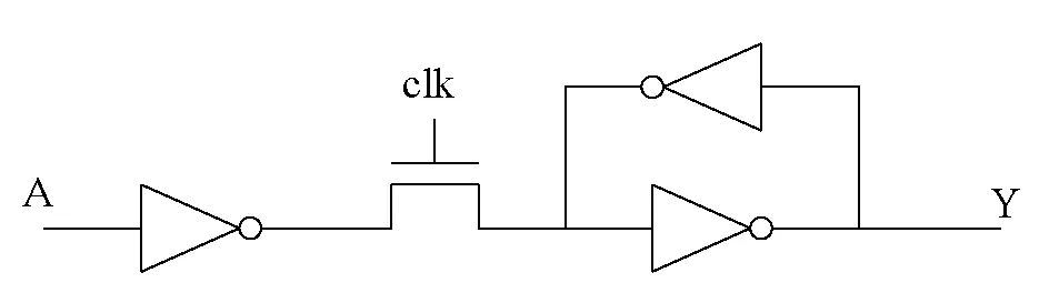
The question (FN19-9, p21, in the paper’s words). Joe Engineer is designing a simple pass-transistor latch as shown below.
FN19-9’s pass-transistor latch (p21, redrawn): A drives an inverter, then a pass NFET on clk, then the storage node (unnamed on the paper; this page calls it X), which drives the forward inverter to Y. The feedback inverter, always on, returns Y to X.
The exam’s own figure (FN19-9, p21)
What went wrong, and the fix (10 points)
FN19-9, p21. He finds that he is unable to write the latch; that is, when clk is high, Y is not affected by the value of A. What has gone wrong? How can this be fixed? (10 points)
Hint
What it asks. A diagnosis and a cure, in words, for a latch whose output ignores its input while it should be transparent. “Unable to write” and “Y is not affected by the value of A” say the storage node never changes enough to flip the forward inverter. The paper gives no sizes, so the answer is an argument; a divider estimate with typical sizes makes it concrete.
The idea. The feedback inverter is not clocked, so it is still on while clk is high, and it drives X toward the old value. To write, the driver inverter must pull X the other way through the pass NFET, and win: pull X past the forward inverter’s threshold before clk falls. The writer is two devices in series, one of them a pass NFET (which is a weak pull-up); the holder is one device. With ordinary sizes the holder wins, X stalls on the old side of , Y never changes, and when clk falls the loop restores the old value completely. Nothing is wrong with the logic: with clk high, , as a latch should be.
Why this formula. Treat each conducting device as a resistor (Chapter 13 §7). While the fight lasts, the same current flows from through the pull-up side, X and the pull-down side to ground, so X sits where the resistances divide the supply: . Writing a 0 into X (A = 1) puts the driver’s NFET and the pass NFET in series on the pull-down side against the feedback inverter’s PFET; writing a 1 (A = 0) puts the driver’s PFET and the pass NFET, pulling up, in series against the feedback inverter’s NFET. The write succeeds only if crosses , that is, if the writer’s resistance is the smaller. The estimate is rough, since transistors are not linear resistors, but it compares strengths, which is all the question needs. Two facts make writing a 1 the worse direction: the pass NFET pulls up weakly (about ), and it cannot lift X above at all. The tempting fixes that fail: a stronger forward inverter (it does not fight, its input draws no current), or a wider pass NFET alone (the driver is in series with it).
FN19-9
- The logic is right. With clk = 1, A passes through two inverters to Y, so Y should equal A. The failure must be electrical: X does not move far enough.
- Who drives X while clk = 1. Three things touch X: the pass NFET (from the driver), the feedback inverter’s output, and the forward inverter’s gate (which draws no current). So two outputs fight over X: the driver through the pass NFET, and the always-on feedback inverter.
- Sizes for an estimate added. The paper gives none; take Chapter 13’s “normal” sizes: every inverter 2/1 (PFET 2 µm, NFET 1 µm) and a 1 µm pass NFET.
- Writing a 0 into X (the latch holds X = 1, Y = 0; A rises). The pull-down is the driver’s NFET and the pass NFET in series, ; the pull-up is the feedback PFET, gate Y = 0, . So , above : X never gets low enough, and Y stays 0.
- Writing a 1 into X (the latch holds X = 0, Y = 1; A falls). The pull-up is the driver’s PFET, , in series with the pass NFET pulling up, : . The pull-down is the feedback NFET, gate Y = 1, . So , far below : worse. And even with no fight the pass NFET could lift X only to (for example, with this guide’s values V and V, only to 0.7 V).
- When clk falls, the pass NFET turns off and the feedback inverter pulls X back to its full old level. Y never follows A: exactly what Joe sees.
- Fix 1: weaken the feedback inverter. Because the holder must lose in both directions: writing a 0 needs , a feedback PFET narrower than 1 µm; writing a 1 needs , a feedback NFET narrower than 1/3 µm. Narrower than a minimum device, so in practice it is made long, or with a series device, as Chapter 11’s half latch is. Chapter 13’s 0.5/0.25 µm feedback inverter writes a 0 at and a 1 at : barely.
- Fix 2: strengthen the write path. A wider driver, and a transmission gate instead of the lone pass NFET: its PFET pulls X up strongly and all the way to . This helps, but it is still a ratio: whether it wins depends on the sizes (Variation 6 shows a transmission gate alone is not enough against a 2/1 feedback inverter).
- Fix 3, the robust one: gate the feedback. Put a second switch in the loop, on , so that the feedback is cut while clk = 1 and reconnected while clk = 0; make both switches transmission gates (Chapter 13 §8). Now nothing fights the write in either direction, full levels pass both ways, and no ratio has to hold at every corner. This is the standard-cell latch, at the cost of a few transistors.
Check. Remove the feedback inverter altogether and the circuit becomes Chapter 13’s dynamic latch, which writes with no fight at all: so the feedback inverter, and nothing else, is what stops the write. The estimate also agrees with the lecture’s own words, given with no numbers: the write path’s NFET “has to overpower the PFET of this feedback path” (Lecture12, 44:43), or the latch “might not be writable” (45:19); and it agrees with Chapter 11’s half latch, a keeper made weak, about a tenth of the pull-down’s strength, for the same reason.
Answer: The feedback inverter is always on, so while clk is high it fights the write; the driver inverter through the pass NFET is too weak to pull the storage node past the forward inverter’s threshold, so Y keeps its old value and the loop restores it when clk falls. Writing a 1 is the worse case: the pass NFET pulls up weakly and only to . Fixes: make the feedback inverter weak (narrow or long, about a tenth of the write path’s strength); strengthen the driver and use a transmission gate; or, best, gate the feedback with (a clocked inverter or a transmission gate in the loop), so nothing fights the write.
Remember. An always-on feedback device must be overpowered by the write path, in both directions; the cure that does not depend on sizes is to switch the feedback off while writing.
The answer key agrees
4. PS5-Q2: a two-bit counter with a synchronous reset
You need
An edge-triggered flip-flop (Chapter 13 §10). Two latches in a row on opposite clock phases. The flip-flop samples D when its master closes and shows it at Q when its slave opens, both at one clock edge. With the master transparent while clk = 0 and the slave while clk = 1, that edge is clk’s rising edge (Chapter 13’s drawing has the phases the other way round, a falling-edge flip-flop). A static master–slave flip-flop with gated feedback gives both Q and , and holds its state however slowly the clock runs.
The flip-flop’s timing (Chapter 13 §3, §11). D must be stable from before the edge until after it; Q changes after the edge. A path from one flip-flop’s output, through logic, to another’s input must fit in a cycle: (the long path), and must not change D too soon after the edge: (the short path, here with one clock and no skew).
Counting in binary (Chapter 15 §11). Adding 1 to flips always, and flips when the carry out of bit 0 is 1, that is when .
The question (PS5-Q2, p3, in the handout’s words). This is a small design problem. Design a two-bit wrap-around counter. The counter counts from “00” to “11” and then begins again at “00.” The systems takes as input a single clock and a synchronous input reset which resets the counter back to “00” when active. You may assume that reset arrives 20 psec after the rising edge of the clock. The clock is 50% duty cycle with 20-psec rise and fall times. The outputs are the two bits of the counter. Design your circuit for the fastest clock frequency possible and verify this maximum frequency of operation with Spectre. You do not have to layout your design.
The problem set gives no points and no figure. The Spectre search is beyond a written exam and is left out (the plan’s scope): the two parts below are the logic and the reset’s timing, which a final could ask on paper. The state diagram is drawn from the words.
PS5-Q2’s counter as a state diagram added, drawn from the handout’s words: the states are , and R is the handout’s reset. With reset low () each rising clock edge counts 00 → 01 → 10 → 11 → 00; with reset high () every state goes to 00.
Part (a): the counter’s logic
PS5-Q2, p3 (the logic). Design a two-bit wrap-around counter. The counter counts from “00” to “11” and then begins again at “00.” […] a synchronous input reset which resets the counter back to “00” when active.
Hint
What it asks. A circuit: two flip-flops holding and the logic that computes their next values, so that each rising clock edge moves the count one step, 00 → 01 → 10 → 11 → 00, and a high reset sends it to 00 at the next edge instead. “Synchronous” is the word that sets the method: the reset acts through the flip-flops’ D inputs, at a clock edge, like any other data; it never reaches into the stored nodes.
The idea. A counter is a state machine whose state is the count. Write the state table (present state and reset → next state), read off one Boolean equation per bit, add the reset as an AND with , then turn the equations into the fewest gate levels, since the problem asks for the fastest clock. The flip-flops are two rising-edge static flip-flops on the one clock.
Why this formula. The equations come from binary addition, . Adding 1 to the low bit always flips it: . The high bit takes the carry out of the low bit, which is : it flips exactly when , so . From 11 both bits flip, to 00: the wrap-around comes for free, with no extra term. A synchronous reset forces the next state to 00 whatever the present state, so each bit is ANDed with . For the gates, De Morgan does the work: is , and is . Why not a reset that clears the flip-flops directly? That would be asynchronous: it would act the moment reset arrives, 20 ps after an edge, in the middle of a cycle, which is not what “synchronous” asks for.
PS5-Q2(a)
-
The state table. Because the count is the state, list each present state with
resetlow and high:next, reset = 0 next, reset = 1 00 01 00 01 10 00 10 11 00 11 00 00 -
Bit 0. It flips every cycle: ; with the reset, . One NOR2.
-
Bit 1. It flips when : ; with the reset, . An XNOR2 and a NOR2.
-
One gate level for bit 1 (for speed). Because the flip-flops give both and , write and build as one complementary gate: a pull-down of
resetin parallel with ( in series with ) and ( in series with ), and its dual as the pull-up. One stage instead of two, at the cost of a three-high PFET stack. -
The flip-flops. Two rising-edge static master–slave flip-flops on the single clock, and as the outputs, and both used by the logic. Static, so the counter keeps its state at any clock speed; a dynamic or TSPC flip-flop would be faster but would add a minimum frequency and, for TSPC, an inverted output (Variation 5).
PS5-Q2’s counter added: two rising-edge flip-flops on one clock, with R for reset. and , so a high reset loads 00 at the next edge.
Check. Run the equations from 00 with reset low: goes 0, 1, 0, 1, 0 and takes each time: 00 → 01 → 10 → 11 → 00 ✓. With reset high, both NORs have a 1 on an input and give 0, so every state goes to 00 ✓. The single complex gate of step 4 agrees with the two-gate form on all eight rows of (, , reset); this page’s test checks all eight.
Answer: , (or one complex gate, ), feeding two rising-edge static flip-flops on the one clock.
Remember. A binary counter is “flip bit 0, flip bit when all lower bits are 1”; a synchronous reset is one more input to each bit’s logic, ANDed in as its complement.
The answer key agrees
Part (b): the reset and the clock
PS5-Q2, p3 (the timing). You may assume that reset arrives 20 psec after the rising edge of the clock. The clock is 50% duty cycle with 20-psec rise and fall times. […] Design your circuit for the fastest clock frequency possible […].
Hint
What it asks. When the reset takes effect, what timing it must meet, and what limits the clock. The handout’s numbers are the reset’s arrival, 20 ps after the rising edge, and the clock’s shape. It gives no device delays (Spectre was to find them), so the frequency below uses illustrative delays, stated as such; the method is what a written exam would test.
The idea. A reset that changes 20 ps after an edge behaves exactly like the output of a flip-flop with a 20 ps clock-to-Q delay: it is launched at one edge and captured at the next. So it must be steady through the current edge’s hold window (it is too late for that edge, which must not see it), and it must reach the flip-flops’ D inputs a setup time before the next edge. The fastest clock is set by the slowest of the three paths into a D input: the counter’s own two loops and the reset’s path.
Why this formula. Each path into a flip-flop obeys the long-path rule , where is when the signal leaves after the edge: for the counter’s bits, 20 ps for reset. Each also obeys the short-path rule , with no skew because one clock drives both flip-flops. Why the reset misses the current edge: if reset reached D within the flip-flops’ hold time after the edge, the edge’s sample would be corrupted, so the design needs , which holds for any ordinary flip-flop. The tempting error is to think a reset “arriving after the edge” acts at that edge: then the count would change mid-cycle, which a synchronous design never does.
reset) enters both NORs directly. Original figure ↑PS5-Q2(b)
- When the reset acts. Because it is sampled like data:
resetrises 20 ps after edge ; edge has already sampled the oldreset, so the counter takes its normal step there. The NORs seeresetat once, D goes to 00, and edge loads 00, which appears after edge . Whileresetstays high, every edge loads 00; after it falls (20 ps after some edge), counting resumes at the following edge, from 01. - The illustrative delays added. For example, with this guide’s values (the handout gives none): ps, ps, ps; a NOR2 35 ps, an XNOR2 60 ps.
- The three paths. Bit 1: ps. Bit 0: ps. Reset: ps. Because the clock must accommodate the slowest: bit 1 is critical, ps, about 5.13 GHz. The reset is not, because it leaves 40 ps before the flip-flops’ outputs do.
- Speeding up bit 1. Because bit 1’s two gate levels set the clock, merge them into the one complex gate of part (a), for example 55 ps: ps, about 6.45 GHz. Bit 0 (135 ps) is now close behind.
- The hold checks. The reset: ps after the edge, against ps, a 40 ps margin. The counter’s own shortest loop, through the NOR: ps, an 80 ps margin. With one clock and no skew, hold is safe.
- The clock’s shape. At a 50% duty cycle each latch of a master–slave flip-flop is transparent for half the period, and at ps a half period is 77.5 ps, of which the 20 ps edges take a quarter. The clock waveform itself, not only the logic, starts to limit the frequency here: that is what the Spectre search would settle.
PS5-Q2’s counter under a reset pattern added, computed from the next-state equations, with R (reset) changing just after an edge (the handout’s 20 ps, drawn as 0.02 of a period) and a little after each edge. The state before edge 0 is unknown (hatched). R rising after edge 5 leaves edge 5’s step alone; edge 6 is the first to see it and loads 00, edge 7 again 00, and edge 8 counts on to 01.
Check. Walk the pattern of the timing figure through the equations: reset high until 20 ps after edge 0, low until 20 ps after edge 5, high until 20 ps after edge 7. Edge 0 samples reset = 1: 00. Edges 1–5 count 01, 10, 11, 00, 01. Edge 6 is the first to see the second reset: 00, and edge 7 again 00. Edge 8 sees reset low: 01. The reset asserted after edge 5 left edge 5’s step alone and acted at edge 6, as step 1 says; this page’s test runs the same sequence. The paths also order sensibly: each ends in the same NOR and setup, so their differences are only their starts and first gates: bit 1’s XNOR (60 ps) against bit 0’s nothing, and (60 ps) against the reset’s 20 ps.
Answer: The reset is sampled like data: asserted 20 ps after edge , it leaves edge ‘s step unchanged and loads 00 at edge . It must meet and . The clock is limited by bit 1’s path, : with the example delays 195 ps (5.13 GHz), or 155 ps (6.45 GHz) with bit 1’s logic merged into one gate.
Remember. Treat a synchronous input that arrives a fixed time after the edge as a flip-flop output with that clock-to-Q: it must meet the next edge’s setup and the current edge’s hold.
The answer key agrees
Variations: storage cells
Two added variations added. Variation 5 is the question the lecturer flagged, “a very good exam question” (Lecture14, 27:02): half latches on the TSPC flip-flop, here made longer, with the flip-flop wired as PS5-Q2’s toggling bit and carried through to the half latch’s size and the slowest clock. Variation 6 gives Joe Engineer a transmission gate and asks, with numbers, whether that is enough.
Variation 5: half latches on a TSPC toggle flip-flop (added)
Variation 5: half latches on a TSPC toggle flip-flop
The question added. The TSPC flip-flop of Lecture 14 (Chapter 15 §6) has three stages. Stage 1: a PFET with gate D, a PFET with gate clk, and an NFET with gate D; output X. Stage 2: a PFET with gate clk from , and an NFET with gate X over an NFET with gate clk; output Y. Stage 3: a PFET with gate Y, an NFET with gate clk and an NFET with gate Y; output . Its output is wired straight back to D, to make bit 0 of a counter (no reset). Stage 2’s NFETs are 2 µm each, the minimum width is 0.4 µm, and a PFET has half an NFET’s strength at equal width. (a) On which edge does the bit change, and does it toggle? (b) With clk low on [0, 2), high on [2, 4), and so on, and at the start, walk X, Y and through three cycles and find when two nodes float at once. (c) Add one transistor that removes that state, and say why it must be weak. (d) Size it by the one-tenth rule, using minimum-width devices. (e) floats while clk is low; it has 4 fF, leaks 0.8 nA, and is read correctly while it has drooped less than 0.1 V. What is the slowest clock? (f) The wiring changes D right after each edge. Is that a hold problem?
Hint
What it asks. Six steps on one circuit: its function with the feedback wire, a walk through its clock phases, the lecturer’s half-latch question, the half latch’s size, the leakage limit on the clock, and a race. The unfamiliar part is the wiring: D is not an independent input but the flip-flop’s own output, so the data changes right after every edge, and that decides which states the flip-flop visits.
The idea. Walk the stages exactly as Chapter 15 does: in each phase, ask of each node whether its pull-up or its pull-down conducts. Stage 1 can only pull X down while clk is high (its clocked PFET is off); stage 2 can only pull Y down while clk is high and is precharged while clk is low; stage 3 inverts while clk is high and can only pull up while clk is low. With the output fed back, every edge that samples D = 1 is followed at once by D falling, which is the sequence that leaves X and Y both floating. A weak device that holds Y high, switched on by the output in exactly that state, removes it.
Why this formula. Four relations, each Chapter 15’s or Chapter 11’s.
- The function (Chapter 15 §6): at each rising edge, a positive-edge, inverting flip-flop. With : , the bit flips at every edge. A designer who reads the output as Q and adds an inverter to make a toggle gets a bit that never changes.
- The half latch (Chapter 15 §5): the device that drives the floating inner node to the value it must keep (a PFET for a 1), gated by the output so that it is on exactly in the dangerous state.
- Its size (Chapter 11 §9): about one tenth of the strength of the network that must overpower it, because when Y has to discharge, stage 2 fights it until the output turns it off. Series devices add resistance, so two equal devices in series act like one of half the width.
- The slowest clock (Chapter 15 §1): a floating node droops by , so it holds for ; it floats for half a period at 50% duty, so .
Variation 5
- (a) The function. Because the flip-flop gives at each rising edge and : the output toggles at every rising edge. It is a divide-by-two, bit 0 of a counter.
- (b) clk low, [0, 2). . Stage 1: the NFET with gate D is on, so X = 0, driven. Stage 2 precharges: Y = 1, driven. Stage 3: its PFET (gate Y = 1) and its clocked NFET are off, so floats at 1.
- (b) Edge at 2. X = 0, so stage 2’s pull-down stays off and Y stays 1; stage 3 now inverts: falls to 0, driven. So D falls. In stage 1 the NFET turns off and the PFETs cannot conduct (the clocked one is off): X floats at 0. In stage 2 the precharge is off and the X-NFET is off: Y floats at 1. From 2 to 4, X and Y both float.
- (b) clk low, [4, 6). D = 0, so stage 1 drives X = 1; Y is precharged, 1; floats at 0.
- (b) Edge at 6. X = 1, so Y discharges to 0; stage 3’s PFET turns on: rises to 1, D rises, and stage 1’s NFET pulls X down to 0. Now Y’s pull-down is off again (X = 0) and its precharge is off: Y floats at 0, alone. From 6 to 8, one dynamic node.
- (b) The pattern. [8, 10) repeats [0, 2), and the edge at 10 repeats the edge at 2: X and Y both float again on [10, 12). The two-node state comes in every other high phase, each time the bit falls from 1 to 0, so this counter visits it constantly.
- (c) The half latch. In that state Y floats at 1 while . A weak PFET from to Y with its gate on is on exactly then and holds Y at 1, so only X floats. It must be weak because of the other edge (step 5): there is still 0 when Y must discharge, so the half latch is on and stage 2 must overpower it until rises and turns it off.
- (d) Its size. Stage 2’s pull-down is two 2 µm NFETs in series: like one NFET of µm. One tenth of that is a 0.1 µm NFET’s strength, and a PFET needs twice the width: 0.2 µm. That is below the 0.4 µm minimum, so use two minimum PFETs in series, which act like one of 0.2 µm: the one gated by at minimum size (it loads the output), the other with its gate tied to ground, always on (Chapter 11’s series device).
- (e) The slowest clock. 500 ns. Because floats for half of each period: s, so 1 MHz. A clock stopped for testing or power saving loses the count.
- (f) The race. D changes only when changes, and changes only after stage 2 has decided: at the edge at 2, Y never had to move, and D falling cannot raise X (its clocked PFET is off); at the edge at 6, D rises only because Y has already fallen far enough to switch stage 3. The feedback is self-timed, so no hold failure, provided Y falls well below stage 3’s threshold before X cuts the discharge off. The half latch slows that discharge, another reason it must be weak.
Variation 5(b)‘s walk added, computed from a switch-level model of the three stages with D wired to , ideal edges: toggles at each rising edge (2, 6, 10), and on [2, 4) and [10, 12), each time it falls, X and Y both float (shaded) unless a half latch holds Y.
Variation 5’s circuit with its answer to (c) and (d) added: Lecture 14’s TSPC flip-flop (Lecture14 @ 27:24) with wired back to D, stage 2’s NFETs 2 µm each, and the half latch on Y: two 0.4 µm PFETs in series from , the upper always on (gate to ground), the lower gated by . Widths in µm.
Check. The walk can be checked against Chapter 15’s table for the flip-flop, which lists the two-node state as “D was 1 at the edge, then fell to 0”: in the toggle wiring D falls right after every edge that samples a 1, so that row is visited at the edges at 2 and 10, and the row “D was 0 at the edge, then rose” (only Y dynamic) at the edge at 6 ✓. This page’s test runs a switch-level model of the three stages with D wired to : is 1, 0, 1, 0 after the edges; X and Y float together only on [2, 4) and [10, 12) without the half latch, and never with it. The size checks by resistance: two 0.4 µm PFETs in series, , against the stage-2 stack’s : one tenth ✓.
Answer: (a) Rising edge; it toggles. (b) X and Y both float on [2, 4) and [10, 12), every other high phase (whenever falls from 1 to 0); [6, 8) leaves only Y floating. (c) A weak PFET from to Y, gate on ; weak because stage 2 must overpower it whenever Y discharges. (d) 0.2 µm, built as two 0.4 µm PFETs in series. (e) MHz. (f) No: the output, and so D, changes only after stage 2 has evaluated.
Remember. To place a half latch: walk the stages, find the phase and data sequence that leave two nodes floating, and hold the inner one at its value with a weak device gated by the output. An output fed back to the input chooses which sequences the circuit actually visits.
Variation 6: a transmission gate against an ungated feedback inverter (added)
Variation 6: a transmission gate against an ungated feedback inverter
The question added. Joe Engineer tries again. He keeps every inverter of FN19-9’s latch at 2/1 µm (driver, forward and feedback) and replaces the pass NFET by a transmission gate: an NFET of 1 µm on clk and a PFET of 2 µm on . Use the course’s resistor model: an NFET of width pulls down as and up as about ; a PFET pulls up as and down as about ; . (a) Can he write a 0 now? A 1? (b) He shrinks the feedback inverter, keeping its 2:1 ratio (PFET , NFET ). For a margin of , X reaching when writing a 0 and when writing a 1, how small must be? (c) Can he build it with a 0.4 µm minimum width? (d) How small would have to be in the original FN19-9 latch, with the lone 1 µm pass NFET? (e) Compare the transistor count with the gated-feedback standard cell, and say which he should use.
Variation 6’s latch added: FN19-9’s circuit with the pass NFET replaced by a transmission gate, an NFET of 1 µm on clk in parallel with a PFET of 2 µm on . Every inverter is 2/1 µm (PFET/NFET); the feedback inverter is still always on.
Hint
What it asks. Whether the transmission gate, which fixes the NFET’s weak high, also wins the fight; then the feedback size that makes the write work in both directions with a margin; then a comparison with the original latch and with the cure that removes the fight. The phrase “with a margin” turns a yes-or-no test into a sizing inequality.
The idea. A transmission gate helps both directions: in each, one of its devices is the strong one. But the write is still a ratio: the writer (driver plus gate, in series) against the holder (the feedback device that is on in the old state). Whether it wins depends on sizes, so the feedback inverter must be made weak enough, and the margin says how weak.
Why this formula. The divider of FN19-9: . Two more facts. Devices in parallel combine like resistors in parallel, , so the transmission gate’s resistance is that of its two devices together in each direction, each with its own strength for that direction (the course’s model, Chapter 11 §2). And a feedback inverter of width pulls with (its NFET, holding a 0) or (its PFET, holding a 1): the 2:1 ratio makes both the same. Setting the divider to the margin gives a closed form: writing against through a writer of resistance comes within of the new rail only if , with here. The model is rough, since devices are not linear resistors, which is exactly why a design adds a margin.
Variation 6
- (a) The gate’s resistances. Pulling down: the NFET, , in parallel with the PFET, : . Pulling up: the NFET, , in parallel with the PFET, : also .
- (a) The write paths. Because the driver is in series with the gate: down, its NFET plus is ; up, its PFET plus is also . The 2/1 feedback inverter holds with either way.
- (a) The verdict. Writing a 0: , above . Writing a 1: , below . Neither works: the transmission gate alone does not beat a full-size feedback inverter.
- (b) The margin. Writing a 0, X must fall to : , so 0.4 µm. Writing a 1, X must rise to against the feedback NFET’s : the same writer resistance gives the same bound, µm.
- (c) Buildable. A 0.8/0.4 µm feedback inverter is exactly minimum width: yes, with no margin to spare on the sizing.
- (d) The original latch. Writing a 0 its path is : 0.333 µm. Writing a 1 it is (the weak NFET pull-up): 0.222 µm, about half the minimum width, so a long or series feedback device would be needed. The transmission gate’s real gain is in the write-1 direction.
- (e) The count. The transmission-gate input with ungated feedback: 6 transistors (plus the driver). The gated-feedback standard cell: 8, 10 with an output inverter. Two more transistors buy a write with no fight in either direction, no fight current, full levels, and no ratio that a slow corner can break. He should use the standard cell.
Check. At µm the divider gives exactly the targets: writing a 0, ✓; writing a 1, ✓. The two directions come out equal because the writer is symmetric ( both ways) and the 2:1 feedback inverter is too; in the original latch the writer is not ( down, up), and the bounds differ. As a limit, with no feedback at all () both directions reach the rail, as Chapter 13’s dynamic latch does.
Answer: (a) No: X reaches only writing a 0 and writing a 1. (b) µm in both directions: a 0.8/0.4 µm feedback inverter. (c) Yes, at minimum width. (d) µm (write 0) and 0.222 µm (write 1): below minimum. (e) 6 transistors against 8 (10 with an output inverter); the gated cell removes the fight and is the one to use.
Remember. A stronger switch narrows the fight but does not end it: an always-on feedback inverter must still be sized weak, for both directions, with margin. Gating the feedback ends it for two transistors.