8. Logical effort and path sizing
Lecture 7 ended with one gate: its delay is its gain times . Lecture 8 strings gates together into a path and asks the designer’s question: given the load at the end and the gate at the start, how big should every gate in between be, so that the path is as fast as possible? The answer is short and powerful. Multiply the gains together and you get a number, the path effort , that does not depend on the sizes at all; the delay is smallest when every stage has the same gain, . From there the lecture finds the best number of stages (a gain of about 3 to 4 per stage, the reason FO4 is the industry’s yardstick), works a full example from 6.86 ns down to 756 ps, and then shows what breaks when a path branches. It closes with the reason, promised in Lecture 7, why the device at the bottom of a stack is slow.
After this chapter you can:
- find any gate’s gain by replacing it with its normalized inverter and dividing its load by that inverter’s input;
- write a path’s delay as and its path effort as ;
- explain why is fixed when the input and output capacitances are fixed and nothing branches, and why the delay is then smallest with equal gains ;
- choose the number of stages (a gain near , in practice 3–4 per stage) and say where added inverters belong and why;
- size a path backwards from the load for equal gains, and estimate its delay before and after;
- compute the branching effort, explain why it makes depend on the sizes, and retune a path around a branch;
- explain why the device furthest from the output in a stack switches slowest, and use it to choose pins.
Boxes and equations marked board were written in the lecture. Parts marked added are explanations or examples this guide adds.
Symbols
| Symbol | Meaning | Unit | First appears |
|---|---|---|---|
| the fan-out-of-one delay: a balanced inverter driving a copy of itself; for a 2W/W inverter | ps | Before you start | |
| , | the “resistance” of a 1 µm NFET or PFET; a device of width has | kΩ·µm | Before you start |
| gate capacitance per micron of width | fF/µm | Before you start | |
| a device width; “2.4/1.2” is a PFET 2.4 µm over an NFET 1.2 µm | µm | §1 | |
| logical effort: a gate’s input capacitance over that of an inverter with the same drive | — | §1 | |
| electrical effort: the capacitance a stage drives over its own input capacitance | — | §1 | |
| the gain (stage effort) of stage ; the stage’s delay is | — | §1 | |
| the input capacitance of the whole path (fixed) | fF or µm of gate | §2 | |
| ; | the input capacitance of stage 2, 3, …; of gate | fF or µm of gate | §2; §3 |
| , | the load at the end of the path | fF or µm of gate | §2 |
| path effort, | — | §2 | |
| , | ; | — | §2 |
| (or ) | the number of stages | — | §3 |
| the equal gain that minimizes the delay | — | §3 | |
| the gain per stage of an inverter chain | — | §4 | |
| a capacitance hanging off the path (a branch) | fF | §8 | |
| , | branching effort of one node; the product over all branches | — | §8 |
Before you start
You need these ideas from Chapter 7. Each is restated here.
- The delay model. A pull-down of width has “resistance” (kΩ), a gate input of width has capacitance (fF), and delay = resistance × load capacitance (1 kΩ × 1 fF = 1 ps). Drain capacitance is ignored.
- The unit of delay. , the delay of a 2W/W inverter driving a copy of itself, whatever is.
- Loads as widths. Every gate input is per micron, so a load “is” microns of gate. At 2 fF/µm, 1 pF is 500 µm.
- The stack rule. devices in series, each times wider, have the strength of one device.
- Logical effort, electrical effort and gain. A gate sized for an inverter’s drive has a larger input: , , . Its electrical effort is . Its delay is .
Notation. A size written “2.4/1.2” means a PFET 2.4 µm and an NFET 1.2 µm wide, as on the boards. is the gain (the board also says “stage effort”) of stage , and the path effort. is the input capacitance of the whole path, those of later stages, and the final load. , and (Section 8) are the names in Sutherland and Sproull’s book; the boards write the products out.
1. A gate’s gain from its normalized inverter
The idea. Replace the gate by the inverter that has the same drive, its normalized inverter. The gate’s gain is the capacitance it drives divided by that inverter’s input capacitance.

The recap
The lecture opens with Lecture 7’s NAND (00:26) board: every device 2 µm, so the two series NFETs act like one 1 µm NFET and each PFET alone matches a 2 µm PFET. It has the drive of a 2/1 µm inverter. Driving one NAND of the same size it sees 4 µm of gate; the 2/1 inverter’s input is 3 µm; the delay is (01:24). Driving two such NANDs (02:00):
The 2 is the electrical effort , the capacitance driven divided by the gate’s own input capacitance, ; the is the logical effort . Their product is the gain, also called the stage effort (03:00) board. (At 02:13 the lecturer calls the 2 “the logical effort”; the board, and his definition a few seconds later, put under the 2.)
The quick way: the normalized inverter
“A quick and easy way to calculate the gain of a stage” (03:15): replace the gate by its normalized inverter, the inverter with the same drive strength, and divide the total capacitance the gate drives by that inverter’s input capacitance.
The NAND driving two NANDs, in one shot (03:15–04:08)
- Normalized inverter of the NAND: a 2/1 µm inverter, input .
- Total load: two NAND inputs, .
- Gain , delay : the same answer as .
Why it works added: the gate pulls down like the normalized inverter’s NFET, , so its delay is . With that is : the load over the normalized inverter’s input. You never need and separately.
How to find the normalized inverter. added Find the strength of each network for a single input switching (the worst case), using the stack rule:
- NAND: the NFETs are in series, so NFETs of width act like one of ; a PFET alone acts like itself.
- NOR: a single NFET acts like itself; the PFETs are in series, so of width act like .
- A balanced gate’s normalized inverter is then “2W/W”: its input is , with the equivalent NFET width.
Worked example. added A NAND with all four devices 3 µm drives 20 µm of gate. The two NFETs in series act like 1.5 µm; one PFET is 3 µm: the normalized inverter is 3/1.5, input 4.5 µm. Gain . Check with : the NAND’s input is , so , and .
Equal-strength technologies. added Some exams state that the NFET and PFET have the same drive. Then the balanced inverter is W/W (input ), , a NAND2 is NFETs , PFETs (), and a NOR2 is NFETs , PFETs (). The normalized-inverter rule is the same; divide by instead of .
Common mistakes.
- Dividing by the gate’s own input capacitance. That gives , not the gain; the gate’s input is larger than its normalized inverter’s by the factor .
- Counting only the on-path load. The gain uses everything the output drives (Section 8).
Check yourself A gate's pull-down is two series pairs of NFETs, the pairs in parallel (A·B + C·D); its pull-up is two parallel pairs of PFETs in series. Every NFET is W and every PFET 2W, with Rpfet = 2Rnfet. Find its normalized inverter, its logical effort, and its gain when it drives a 2-input NAND whose devices are all W.
This is the AOI22 of Chapter 7. A single input switching sees a stack of two in either network: the NFETs act like , the PFETs like . The normalized inverter is over , input . One input drives an NFET and a PFET : , so . The NAND’s input is , so the gain is . (MT17-5 uses exactly this gate as its second stage.)
2. Path delay and path effort
The idea. A path’s delay is the sum of its gains. Their product, the path effort , depends only on the gate types and on the capacitances at the two ends of the path, not on how the gates in between are sized.
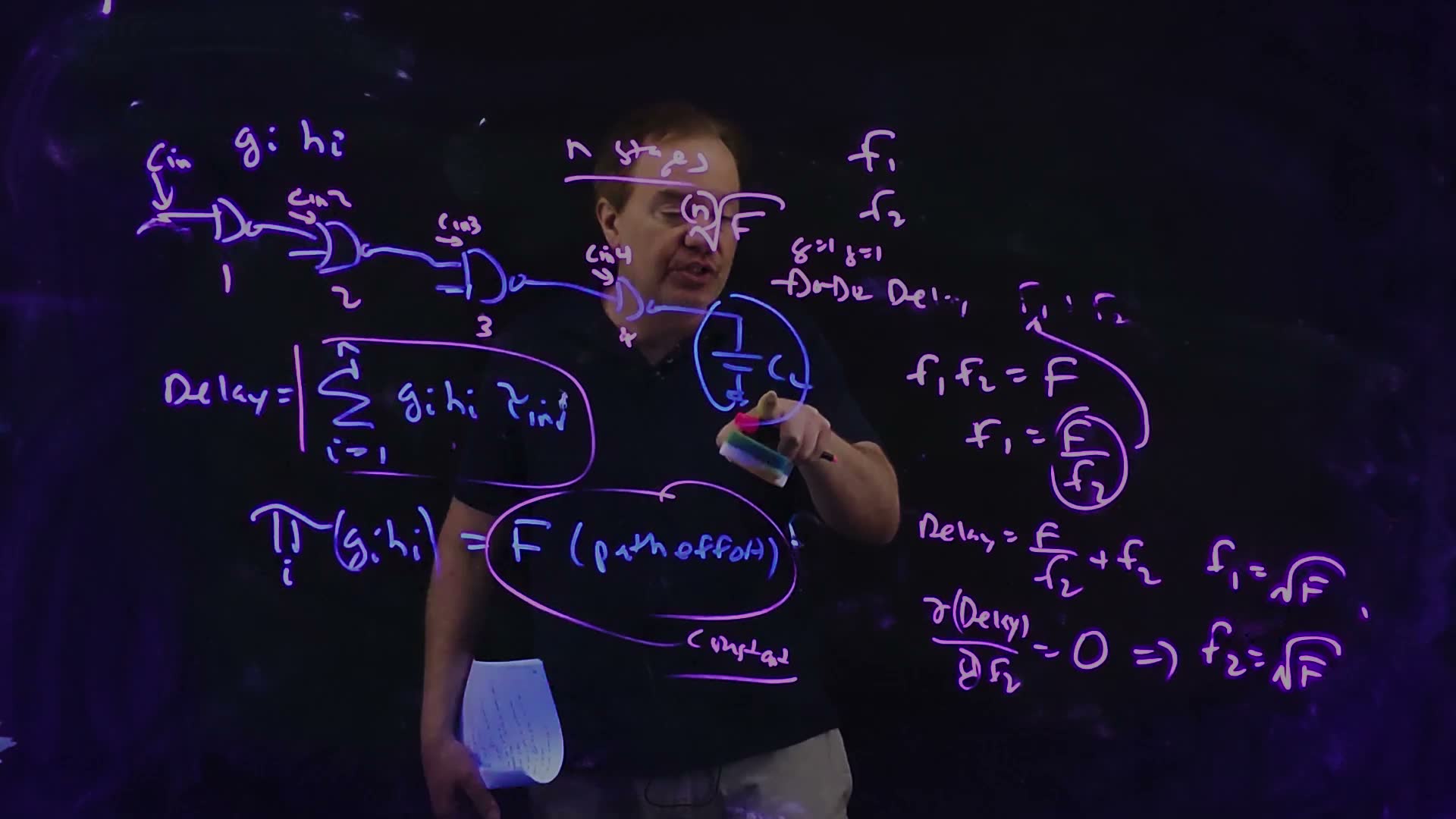
The board’s four-gate path (redrawn from Lecture08 @ 09:59): an inverter, a NOR, a NAND and an inverter between and , each gate driving only the next. is the path’s input capacitance; , and are those of gates 2, 3 and 4.
The board (Lecture08 @ 09:59)

Fair copy of the board above (Lecture08 @ 09:59), mark for mark in its own layout. Black is the blue pen. Magenta is the pink pen, the second layer: the ellipse and “constant” round , the circle round , and the telescoping product it leads to at the right. The circuit is read from 11:12, where the lecturer doesn’t block it.
Posing the problem
The question (04:20): for a path through combinational logic, how should the gates be sized for the minimum delay? Only delay for now; power matters too, and the lecture comes back to it (04:47). The example path (05:09) board: an inverter, a NOR, a NAND, an inverter, and a final load , with no fan-out: every gate drives exactly one gate (05:39).
Two capacitances must be fixed for the question to make sense (06:09):
- the load at the end, ;
- the input capacitance of the path, . Otherwise you could make every gate enormous and push a huge capacitance onto the path’s input, which is “kind of fake, because somebody’s gonna have to drive that large capacitance” (06:30).
Delay and path effort
Each stage has a logical effort and an electrical effort , so board
Now multiply the stage efforts instead of adding them (07:18). The product is the path effort board:
The path effort is a constant (board, 07:35–09:59)
- .
- depends only on which gates are in the path: here . It is a constant board.
- Each is the capacitance stage drives over its own input capacitance. Without fan-out, stage drives exactly stage ‘s input.
- So board: “cancel, cancel, cancel” (09:30).
- board, fixed because both ends are fixed.
- So is a constant: resize the gates in between however you like, and stays the same (09:59).
(At 09:15 the lecturer says the electrical effort is “the capacitance that I’m driving times my own input capacitance”; he means divided by, as the board’s fractions show.)
Worked example. added For the board’s path (inverter, NOR, NAND, inverter), . If is 64 times , then , whatever the sizes of the NOR, NAND and second inverter.
Common mistakes.
- Forgetting that is over the input of the first gate, not of the last.
- Using when a gate drives anything besides the next gate. Then no longer telescopes (Section 8).
Check yourself A path is a NAND2 whose devices are all 2 µm (its input fixed at 4 µm), then a NOR2, then an inverter, then a load of 360 µm of gate. Rpfet = 2Rnfet. What are G, H and F?
, , .
3. Equal gains minimize the delay
You need
A path and its gains. A path is a chain of gates from a fixed input capacitance to a fixed load , each gate driving only the next one, like the board’s four-gate path below. Stage ‘s gain is . The logical effort is 1 for an inverter, for a NAND2 and for a NOR2 when . The electrical effort is the capacitance the stage drives over its own input capacitance. The quick way to get a gain is the load divided by the input of the gate’s normalized inverter (Section 1).
Path delay. Stage takes , where is the fan-out-of-one delay of an inverter, so the path takes . This section minimizes that sum.
Path effort. The product of the gains is . Because each gate drives only the next, : every inner capacitance cancels. So , with and , whatever the sizes of the gates in between. That needs three conditions: nothing branches off the path; is fixed (otherwise you could make every gate huge and push the delay onto whatever drives the path); and is fixed. This section uses as the constraint: the gains can be traded against each other, but their product cannot change.
The question. Between a fixed input and a fixed load you may resize every gate, but the product of the gains will not move. How should that fixed product be split among the stages so that their sum, the delay, is as small as possible? The lecture’s answer (10:44–12:08): split it equally.
Two stages
The lecture starts with the smallest case (10:44) board: two inverters, each, between a fixed and a fixed .
Two inverters between a fixed input and a fixed load (redrawn from the board, Lecture08 @ 13:36). The only free choice is , the second inverter’s input: it is stage 1’s load and stage 2’s strength.
The board (Lecture08 @ 13:36)
Fair copy of the board above (Lecture08 @ 13:36), mark for mark in its own layout. Black is the blue pen. Magenta is the pink pen, the later layer: the box and the ellipse over the left-hand equations and the whole two-stage derivation at the right. The board’s row Delay is partly rubbed out at 13:36; it is restored here from 12:27.
Two stages (board, 10:44–12:08)
- Write the two gains. Stage 1 drives inverter 2’s input, so . Stage 2 drives the load, so . The delay is board.
- See what is fixed. The only free choice is the size of inverter 2, that is, . Making inverter 2 bigger makes it stronger, so falls; but inverter 2 is then a bigger load for inverter 1, so rises by the same factor. Their product does not depend on board.
- Eliminate . Because the product is fixed, board, and the delay has one variable left: board.
- Set the derivative to zero board. , so . The board writes only “= 0”; the derivative is written out here. The second derivative, , is positive, so this is a minimum added.
- Then . board: the two gains are equal.
- In sizes added. means , so : the middle inverter’s input is the geometric mean of the two fixed ends.
The delay against the split
The derivative says where the minimum is. A plot shows how much an unequal split costs added. Take a concrete chain: inverter 1 is 2/1 µm, so its input is of gate (fixed), and the load is of gate. Then , and three sizes for inverter 2 give three points of the curve:
| Inverter 2’s input | Delay | ||
|---|---|---|---|
| 3 µm (a 2/1 inverter) | 1 | 16 | |
| 6 µm (4/2) | 2 | 8 | |
| 12 µm (8/4) | 4 | 4 |
The two-stage delay against the split, computed from with added. The marked points are the table’s three sizings and their mirror images; the minimum, 8, is at .
Reading the curve.
- The bottom is at , where too: . That is the 12 µm inverter, and , the geometric mean of step 6.
- The curve is symmetric on the log axis. and both give : they are the same split with the two stages swapped. A second inverter that is too big costs as much as one that is too small by the same factor.
- It is flat near the bottom and steep far from it. (inverter 2’s input 16 µm) costs , only 4% more than the best. The split 2 and 8 costs 25% more, and 1 and 16 more than twice the best (17 against 8). Rough balance is nearly as good as exact balance; a badly unbalanced path is very slow.
- Why the steep side. Going from the balanced 4 and 4 to 2 and 8 saves in stage 1 but costs in stage 2. Halving one gain doubles the other, and the doubled gain is the larger one, so it always loses more than the halved one gains.
With the lecture’s ps (Section 5), the three sizings take 816, 480 and 384 ps.
Any number of stages
“In general, if I have stages … I want to take the -th root of the path effort” (12:08) board. The lecture states the rule for stages without proof; here the number of stages is written . The argument below needs nothing beyond the two-stage case added.
Resize one gate, here gate 3, and only two gains move added: , because gate 3 is stage 2’s load, and , because gate 3 is stage 3’s strength. Their product stays fixed. The stages are inverters (), so the product is ; with other gates it is , still fixed.
Why every gain must be equal (added)
- Resize one inner gate and nothing else. Gate ‘s input capacitance appears in exactly two gains. It is on top in , because gate is stage ‘s load. It is underneath in , because gate ‘s size is stage ‘s strength. Every other stage keeps its load and its size, so its gain does not move.
- That pair has a fixed product. , and has cancelled. Resizing gate is therefore exactly the two-stage problem, and the pair’s sum is smallest when .
- The same fact without calculus. For two gains and with a fixed product , , and it is zero only when . So any unequal neighbouring pair can be made faster by resizing the gate between them, and the rest of the path does not notice.
- So at the best sizing every neighbouring pair is equal. If one pair were unequal, step 3 would lower the delay. So , , and so on: all gains are equal. They multiply to , so each is .
- The minimum delay is stages of each: .
What it means physically. In this model a stage’s delay is its gain times , so equal gains mean equal stage delays: no stage is a bottleneck. Every inner gate sits at the size where making it bigger would slow its driver by as much as it speeds up itself.
An example of step 4. A four-stage path with gains 2, 8, 4 and 4 has and takes . Resize gate 2 only: stays fixed, and rebalancing gives 4 and 4. The delay falls to , which is : this path is now at its minimum.
The rule to keep
What breaks it.
- A branch. If a gate also drives something off the path, contains the sizes, and the best gains are no longer equal (Sections 8–9).
- A limit that binds. A gate that would have to be narrower than the minimum width, or a cap on how far a gate may be skewed (FN19-8, FN10-9), takes a width out of your hands.
- A free . If you may add inverters, choose the number of stages too (Section 4: a gain of about 3–4 per stage).
Memorize or derive. Memorize and , with their three conditions. Derive the reason when a question asks you to show it. It takes three lines:
- Two stages with : .
- , so .
- stages: resizing the gate between stages and keeps fixed, so every neighbouring pair is equal, and .
A worked example: the lecture’s path
The lecture’s own example (20:01–29:52) board, the path that Sections 5–7 estimate, resize and extend. It runs from a fixed inverter, 2.4/1.2 µm, through a NAND2 and a NOR2 to a 1 pF load. , and .
The lecture’s example path at gate level (from the board, Lecture08 @ 29:52): a fixed inverter, m (its devices are 2.4/1.2 µm), a NAND2 and a NOR2 driving 1 pF m of gate. The logical efforts are for .
The best delay of the lecture's path (board, 27:40–29:52)
- The gate types give . With , .
- The two fixed ends give . The load in microns of gate is , and the fixed inverter’s input is : .
- The path effort. ; the board writes 308 board. Nothing about the NAND’s or the NOR’s sizes went into it.
- Equal gains. Three stages share it equally: board.
- The delay. . The technology’s ps, so the delay is 973 ps board.
Check. As drawn on the board, the gains were 0.667, 3.33 and 138.9. Their product is also 308.6, because does not depend on the sizes; but their sum is ns. Equal gains make the same three gates about seven times faster. Section 6 then finds the widths that give those equal gains (the NAND all 12.2 µm; the NOR’s NFETs 24.7 µm and PFETs 98.8 µm), and Section 7 adds stages.
Traps.
- Equalizing the wrong thing. The rule equalizes the gains , not the sizes, not the electrical efforts and not the stage capacitances. In the worked example, at equal gains of 6.76 (6.758 unrounded) the inverter’s is 6.76, the NAND’s and the NOR’s : a gate with a larger logical effort gets a smaller electrical effort.
- Using with a branch. It assumes is fixed. A side load makes depend on the sizes (Section 8), and the best gains are unequal (Section 9).
- Speeding up one stage on its own. Enlarging the gate of the slowest stage lowers its gain but raises the gain of the stage before it by the same factor. In the 2, 8, 4, 4 path, making gate 2 four times bigger turns the first two gains into 8 and 2: still . Balance the pair instead.
- Resizing the first gate. Its input capacitance is , the constraint that makes the problem well posed. It is given, not chosen.
Check yourself Two inverters sit between a fixed input of 2 µm of gate and a load of 200 µm of gate. What input should the second inverter have, and what is the delay in τinv? What is the delay if its input is 10 µm instead?
, so each gain should be . The second inverter’s input is the geometric mean, , and the delay is . With 10 µm, the gains are and : , 25% slower.
Check yourself A path is a NAND2 whose devices are all 2 µm (its input, 4 µm, is fixed), then a NOR2, then an inverter, then a load of 360 µm of gate, with Rpfet = 2Rnfet. What gain should each stage have, and what is the minimum delay? A designer instead sizes the NOR and the inverter so that the first two gains are both 4. What is the third gain, and how much slower is the path?
and , so . Equal gains: , and the delay is . With the first two gains at 4, the product still has to be 200, so the third gain is . The delay is , 17% slower.
Check yourself A four-stage path without branches has gains 2, 8, 4 and 4. You may resize only the second gate. What are the best first two gains, and the new delay? Is the path then at its minimum?
Resizing gate 2 moves only and , and their product stays fixed, so the best split is 4 and 4. The delay falls from 18 to . and : yes, all four gains are now .
4. How many stages?
The idea. When the load is large, adding inverters (logical effort 1) lowers the gain each stage must provide. The best gain per stage is ; with drain capacitance it moves toward 4. That is why designers aim for 3–4 per stage, and why FO4 is the standard yardstick.

Adding stages can help
So far was fixed. But you can add stages, and with a very large load that can reduce the delay (12:39). The stages to add are inverters: their logical effort is 1, so they don’t increase (13:07). For the analysis the lecturer uses a chain of inverters only; the result carries over to any path (13:59).
The best gain per stage (board, 14:21–17:37)
- inverters from to , each with the same gain (the best choice, Section 3) board.
- All , so board.
- Take logs: , so board.
- The delay is board. Substitute : board.
- Only depends on . Its derivative is added; setting it to zero board: , .
“So basically alpha is around three” (17:25). Two refinements (17:37–18:58):
- The analysis ignores drain capacitance. With it, the best gain “creeps up to be something closer to four”, and that is why FO4 is the metric: in a delay-optimized design, each stage has a gain of about four board (“α ≈ 3 ↑ 4”).
- The minimum is shallow: 3.5, 4 or even 4.2 make little difference. Tune each stage’s gain to roughly 3–4, then choose the number of stages that achieves it.
How shallow? added The factor is 2.72 at , 2.73 at 3, 2.89 at 4 (6% more) and also 2.89 at 2, but 3.35 at 6 (23% more). Too few stages costs more than one too many.
In practice. added With the best count is about . Then pick a count the logic allows: inverters added to a path must come in pairs, or the function is inverted. Compare for the candidates; the widget of Section 6 plots this curve for the lecture’s example.
Check yourself An inverter chain must drive a load 1000 times its input capacitance. How many stages minimize the delay, what is the gain per stage, and how much slower are 4 stages?
, so about 7 stages. With 7: gain , delay . With 6: ; with 8: ; with 4: , 20% slower. Near the optimum the curve is flat.
5. A worked example: estimating a path
The idea. The lecture’s example path, sized arbitrarily: compute each stage’s gain from its normalized inverter, add them, and multiply by . One badly sized stage dominates.
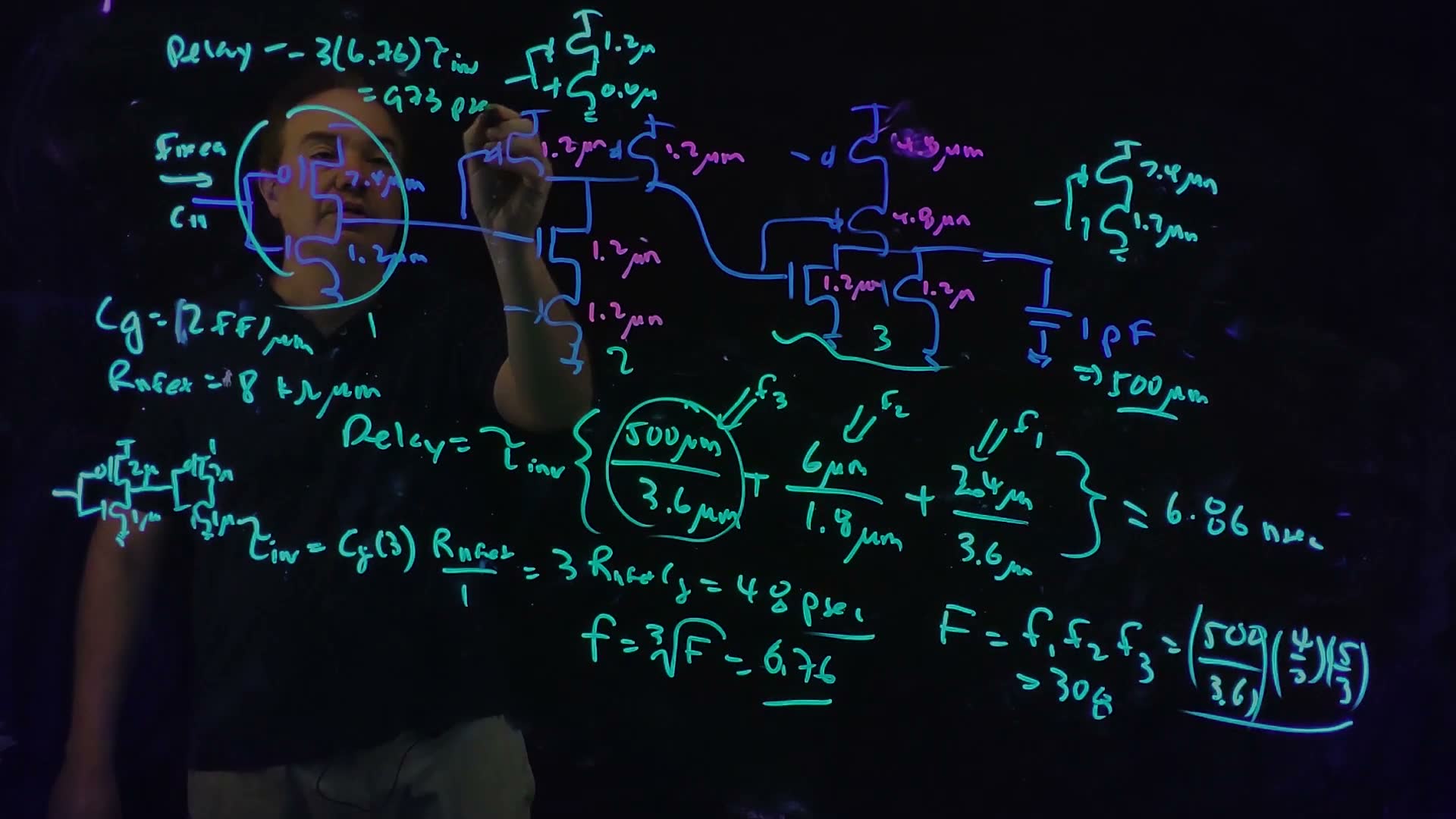
Fair copy of the board above (Lecture08 @ 29:52), mark for mark in its own layout. Black is the circuit: the blue pen, with the device widths in pink. Teal is the cyan pen, the working laid over the circuit: the circle and “Fixed → ”, the stage numbers, the normalized inverters drawn beside the NAND and the NOR, the FO1 pair at the bottom left that sets , the delays, and . The inverter and the NAND, which the lecturer blocks at 29:52, are read from 29:07 and 30:44. † The board truncates to 308; either way.
The circuit
The path (20:01–21:52) board:
- an inverter 2.4/1.2 µm. Its size is fixed: it sets the path’s input capacitance (21:48);
- a NAND with all four devices 1.2 µm;
- a NOR with NFETs 1.2 µm and PFETs 4.8 µm (twice 2.4 µm, because they are a stack of two);
- a load of 1 pF.
“These are just random size choices, and we’ll see how they’re terrible” (21:33).
The gains
“If this were a normal class, the first thing I would be asking is what does one picofarad convert to in microns” (22:10). At , 1 pF is 500 µm of gate board.
Gains from the normalized inverters (board, 23:11–25:05)
- NOR (stage 3). Its NFETs (1.2 µm, one at a time) and its PFET stack (two 4.8 µm devices act like 2.4 µm) give the normalized inverter 2.4/1.2, input 3.6 µm board. It drives 500 µm: gain .
- NAND (stage 2). Its NFET stack (two 1.2 µm act like 0.6 µm) and one PFET (1.2 µm): normalized inverter 1.2/0.6, input 1.8 µm board. It drives one NOR input, : gain .
- Inverter (stage 1). It is already an inverter, input 3.6 µm. It drives one NAND input, : gain .
The delay
The technology (25:20) board: and , so for a perfect 2:1 ratio. The FO1 delay doesn’t depend on the inverter’s size (“a 2000 over 1000 or 2 over 1, fan out of 1 is fan out of 1”, 26:15):
Delay as drawn (board, 26:51–27:13)
- Sum of the gains: .
- Delay board.
The last term dominates (27:13): the NOR “is struggling to drive this 500 microns. It just doesn’t have the drive strength.” This is a poorly tuned path.
Common mistakes.
- Forgetting to convert the load to microns of gate (or to µm at the right ).
- Using the NOR’s own input (6 µm) instead of its normalized inverter’s (3.6 µm) for its gain.
Check yourself In the lecture's path, make only the NOR 10 times larger (NFETs 12 µm, PFETs 48 µm). What are the three gains and the delay?
NOR: normalized inverter 24/12, input 36 µm, gain . NAND: it now drives , gain . Inverter: still . Total : much better than 6.86 ns, but the NAND is now the bottleneck. Every stage has to grow together.
6. Resizing for equal gains
The idea. Compute , take its -th root, and size the gates one at a time from the load back to the fixed first gate, giving each the same gain.
The target
The path effort can be computed two ways (27:40–29:25) board: as the product of the three gains, or as :
added The product of the gains as drawn, , is also 308.6: doesn’t depend on the sizes. Each stage should have the gain board
and the delay becomes board: “from almost seven nanoseconds all the way down to less than one nanosecond” (29:52). (At 28:58 the lecturer says “the cube root of this winds up being 308”; 308 is itself.)

Working back from the load
“We’re gonna do this by starting from the last stage in the path and working our way back” (30:27). For each stage, size its normalized inverter for a gain of 6.76, then translate that into the gate’s devices.
Resizing (board, 31:37–35:29)
- NOR. Its normalized inverter must have input . A third of that is the NFET board: , with a 49.3 µm PFET.
- Translate to the NOR: its NFETs have the normalized inverter’s pull-down strength, 24.7 µm each; its PFETs are a stack of two, so each is twice 49.3, 98.8 µm (“4 times 24.7”) board.
- NAND. It now drives one NOR input: board. Its normalized NFET is (PFET 12.2 µm) board.
- Translate: the NAND’s NFETs are a stack of two, so each is twice 6.1, 12.2 µm; each PFET matches the normalized PFET, 12.2 µm. All four devices are 12.2 µm board.
- The inverter. “Trick question. I don’t” resize it (34:56): its input capacitance is fixed.
- Check board: the inverter drives one NAND input, , and its own input is 3.6 µm: . “If it’s not, I did something wrong” (35:29).
added Without rounding: NOR NFETs 24.66 µm, PFETs 98.65 µm; NAND 12.16 µm; the check gives exactly 6.758. The NOR grew 20 times and the NAND 10 times: the gate driving the big load had to grow, so the gate driving it had to grow too (35:29).
Try it: start from “as drawn”, then press “sized, 3 stages”. Change the load and watch every width follow it while the fixed first inverter stays put.
What to notice.
- As drawn, the gains are 0.67, 3.33 and 138.9: far from equal. Sized, all three are 6.76, and the delay drops from 142.9 to 20.3 .
- is 308.6 in every sizing: only the gate types and the two end capacitances set it.
- The dots on the curve are the delays you can actually have with 3, 5, 7 or 9 stages (Section 7).
Common mistakes.
- Resizing the first gate. Its input capacitance is the constraint that makes the problem well posed.
- Dividing by 3 and stopping. That gives the normalized inverter’s NFET; a stacked network then doubles (NAND NFETs, NOR PFETs).
- Starting from the input end. You only know each gate’s load once the next gate is sized, so work back from the load.
Check yourself Size the path of the check in Section 2 (NAND2 all 2 µm, fixed; NOR2; inverter; 360 µm of gate) for minimum delay. Give the inverter's and the NOR's devices, and check the NAND's gain.
. Inverter: input , so 41.0/20.5 µm. NOR: it drives 61.6 µm, so its normalized input is , NFET ; the NOR’s NFETs are 3.51 µm and its PFETs ; its input is 17.5 µm. NAND: normalized inverter 2/1 µm (input 3 µm), so its gain is . ✓ Delay .
Check yourself Equal-strength technology: τinv = 50 ps, Cg = 1 fF/µm. A path is an inverter 1/1 µm (fixed), a NAND2, an inverter, and 400 fF. Find F, the stage gain, the delay, and the sizes.
With equal strengths the normalized inverter is W/W and . , , , delay . Last inverter: input , so 29.9/29.9 µm. NAND: normalized input , so : NFETs , PFETs , input 13.4 µm. Check: . ✓ (MT23-5b works in this convention; its key prints “1244.7 ns” for about 1.24 ns.)
7. Adding stages, and where to put them
The idea. With a gain of 6.76 the path has too few stages. Two more inverters bring the gain to 3.15 and the delay to 756 ps. Where they go doesn’t change the delay, but next to the load they save a great deal of transistor width.

Five stages
The gain 6.76 is “certainly higher than 3 to 4” (36:19). The path effort is still 308; it didn’t change during the resizing (36:55). Take the fifth root instead (37:01) board:
More than 200 ps faster than three stages, by adding two inverters (37:18). added Unrounded, and the delay is 755 ps. Comparing stage counts for this : 3 stages 973 ps, 5 stages 755 ps, 7 stages 762 ps, 9 stages 817 ps. Five is the best count the logic allows; is where the gain would be exactly .
Where the inverters go
“From a delay point of view, I could have put them either place” (38:19): next to the load, or between the first inverter and the NAND. and are the same, so the delay is the same. But next to the load is “vastly superior … from a power perspective” (39:06):
- the gates closest to the big load are the largest;
- if those are inverters, they are single devices; if they are the NAND and NOR, their big devices come in stacks, doubled in width;
- so the total device width is smaller with the inverters at the load, and with it the area and, above all, the dynamic power of switching the path (40:05).
added The widget above has the numbers: choose “sized, 5 stages” and switch between the two placements. The total transistor width is 289 µm with the inverters next to the load and 805 µm with them after the first inverter, for the same 755 ps. added (Fall 2026 adds the other side of the same trade: a path with slack can be made smaller to save power.)
Sizing the five stages

The procedure is the same as before: work back from the load, each normalized NFET being (load)/(3.15 × 3). The board starts the chain but has an arithmetic slip (41:26): is 52.9 µm, not 16.8 µm. The board’s 16.8 µm is in fact the NFET of the next inverter back, and its 5.32 µm the NOR’s normalized NFET. The corrected chain:
Five stages, corrected (board procedure, 40:46–42:36)
- Last inverter: NFET , so 105.8/52.9 µm; its input is 158.7 µm.
- The inverter before it: NFET , so 33.6/16.8 µm; input 50.4 µm.
- NOR: normalized NFET (the board’s 5.32); NFETs 5.33 µm, PFETs ; input 26.7 µm.
- NAND: normalized NFET ; all four devices ; input 11.3 µm.
- Check: the fixed inverter’s gain is . ✓
“And I can keep repeating this … you can figure out how to do the rest” (42:36). The lecture moves on before finishing the chain; the steps above finish it. The widget of Section 6 (“sized, 5 stages”) uses the unrounded gain 3.147, so its widths differ in the last digit: 106/53.0, 33.7/16.8, NOR 5.35/21.4, NAND 5.66 µm.
Common mistakes.
- Adding an odd number of inverters: the path’s logic function flips.
- Dividing by the gain twice (the board’s slip). Each step divides the stage’s load by once, then by 3 for the NFET.
Check yourself HW3-3 has a path with F = 555.6 and τinv = 24 ps. Compare 3, 5, 7 and 9 stages. Which is best?
: 3 stages , 5 stages , 7 stages , 9 stages . In picoseconds: 592, 425, 414 and 436 ps. Seven stages (four added inverters) is best, at a gain of 2.47 per stage, close to ; . (HW3-3b; its 7-stage row prints 555.7 and “× 3”, typos for 555.6 and × 7.)
8. Branching effort
The idea. When a gate also drives something off the path, the product of the electrical efforts no longer telescopes. A branching factor appears, and because it contains the sizes of the gates, the path effort is no longer fixed.

So far every gate drove exactly one other gate, and that is what made a constant (43:05). With fan-out, “when we resize, we’re actually gonna change … the path effort” (43:52).
The branching effort (board, 44:13–46:41)
- The same path, now with a capacitance (the fan-out) also hanging off stage 2’s output board.
- Stage 2 drives , so .
- board.
- Everything cancels except one factor board: .
- The extra factor is the branching effort (46:41) board, in “the Sutherland and Sproull formalism”.
The trouble (46:58): the branching effort depends on the sizing. It contains , the size of stage 3. So is no longer a constant, and the gains of the best design are no longer all equal (47:24). If the factor becomes 1 and we are back to Sections 2–7.
Worked example. added Take the 3-stage path of Section 6 as sized (NAND all 12.16 µm, NOR NFETs 24.66 µm, PFETs 98.65 µm) and hang 100 µm of extra gate on the NAND’s output. The NAND now drives against a normalized inverter of : its gain jumps from 6.76 to 12.24. The others are unchanged: delay , up from 973 ps. The branching effort is , and .
Common mistakes.
- Leaving the branch out of the stage’s load. The gain uses the total capacitance the stage drives.
- Taking with from the old sizes and treating it as exact. It is a reasonable first guess, but moves as soon as you resize the stage after the branch.
Check yourself In a path, a stage drives the next gate's input of 20 µm and also a 100 µm branch. What is its branching effort? If the next gate is made 30 µm, what does it become?
. With 30 µm: . Making the on-path gate bigger makes the branch a smaller fraction of the load, so (and ) falls. These are the numbers of the lecture’s example in Section 9.
9. Retuning a path with a branch
The idea. With a heavy branch, equal gains are not the best. Enlarge the gate just after the branch: its gain drops a lot, while the gate driving the branch, whose load is mostly the branch, slows only a little. Then rebalance the neighbours.
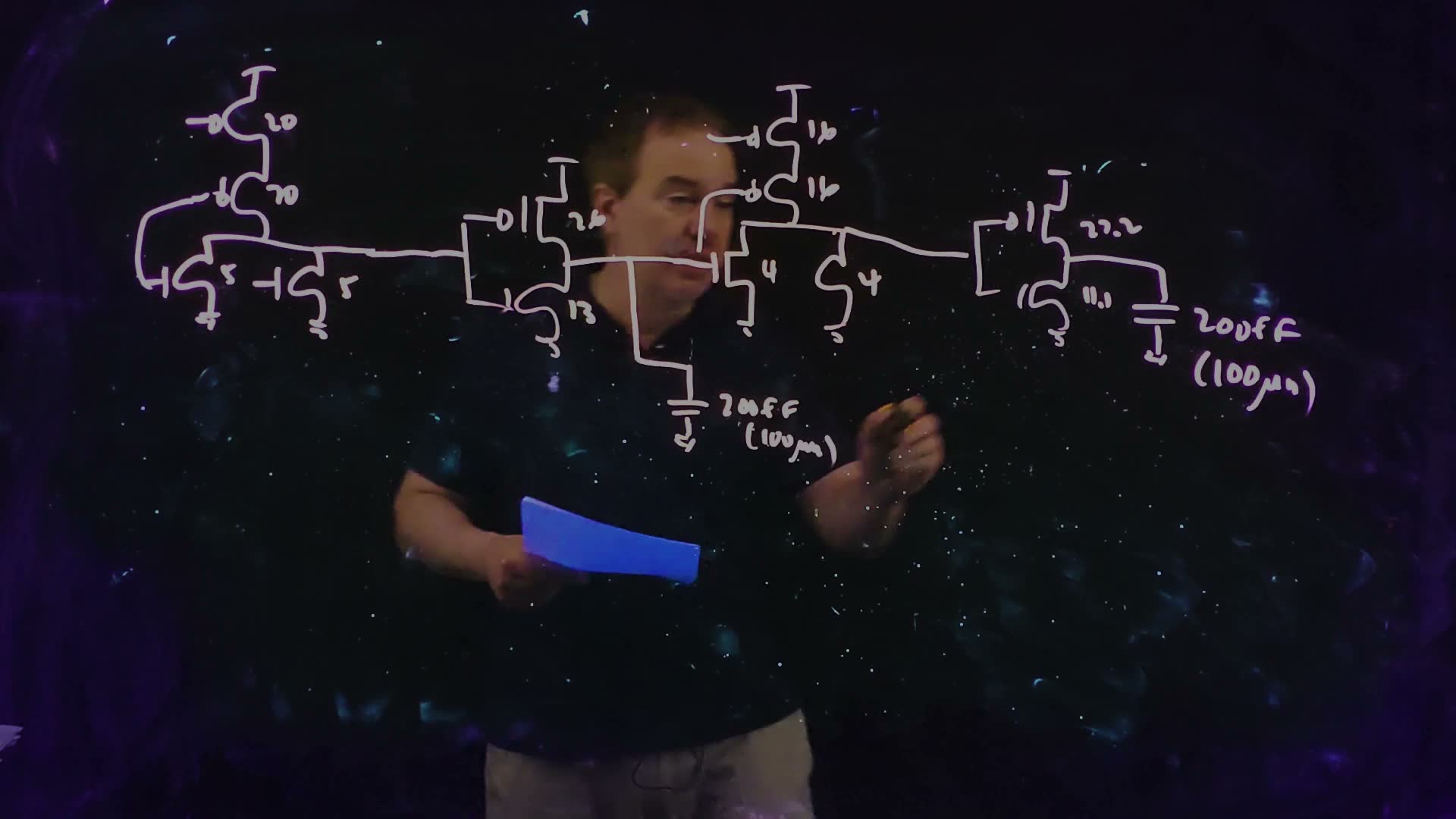
The circuit, with every gain about 3
The example (48:34–50:20) board, at :
- a NOR, NFETs 5 µm, PFETs 20 µm (fixed);
- an inverter 26/13 µm, whose output also drives a 200 fF branch, 100 µm of gate;
- a NOR, NFETs 4 µm, PFETs 16 µm;
- an inverter 22.2/11.1 µm, driving 200 fF, 100 µm.
The sizes were chosen so that every gain is about 3, “and this is 2.7, close to 3” (50:20). “With all the analysis I’ve done today”, that should be optimal, yet it isn’t, “because of the presence of this branching” (50:48). The board’s delay is 11.7 τ_inv.
The gains as drawn (added, from the board's widths)
- Inverter 4: drives 100 µm; its input is : gain .
- NOR 3: drives 33.3 µm; normalized inverter 8/4 (PFET stack of two 16 µm acts like 8 µm), input 12 µm: gain .
- Inverter 2: drives NOR 3’s input, , plus the 100 µm branch: .
- NOR 1: drives inverter 2’s 39 µm; normalized inverter 10/5, input 15 µm: gain .
- Sum: . The board’s 11.7 is , each gain rounded.
Step 1: enlarge the gate after the branch
“If I size this guy up” (51:42) board: NOR 3’s NFETs 4 → 6 µm, PFETs 16 → 24 µm. Its input grows from 20 to 30 µm, but inverter 2’s load only grows from 120 to 130 µm, because most of it is the branch.
| Stage | Board | As drawn (added) |
|---|---|---|
| NOR 3: | 3 → 1.83 | 2.78 → 1.85 |
| inverter 2: | 3 → 3.25 | 3.08 → 3.33 |
| delay | 11.7 → 10.74 τ_inv | 11.45 → 10.79 τ_inv |
“I’m able to drop this gain far more than I increase this gain” (52:00). How far you can go depends on the branch compared with the on-path input; you could do it “analytically and exactly”, but “usually you just sort of look at it” (52:20–53:19).
Step 2: rebalance
Now NOR 3 (1.85) and inverter 4 (3.00) are unequal, with nothing branching between them, so balance them (53:19) board: inverter 4 from 22.2/11.1 to 30/15 µm. Its input is 45 µm, so NOR 3’s gain rises to and inverter 4’s falls to . The delay drops a little further, to 10.63 τ_inv on the board, 10.66 with the widths as drawn. (The board and the speech say 2.27 for inverter 4; , and the board’s 10.63 itself uses 2.22.)
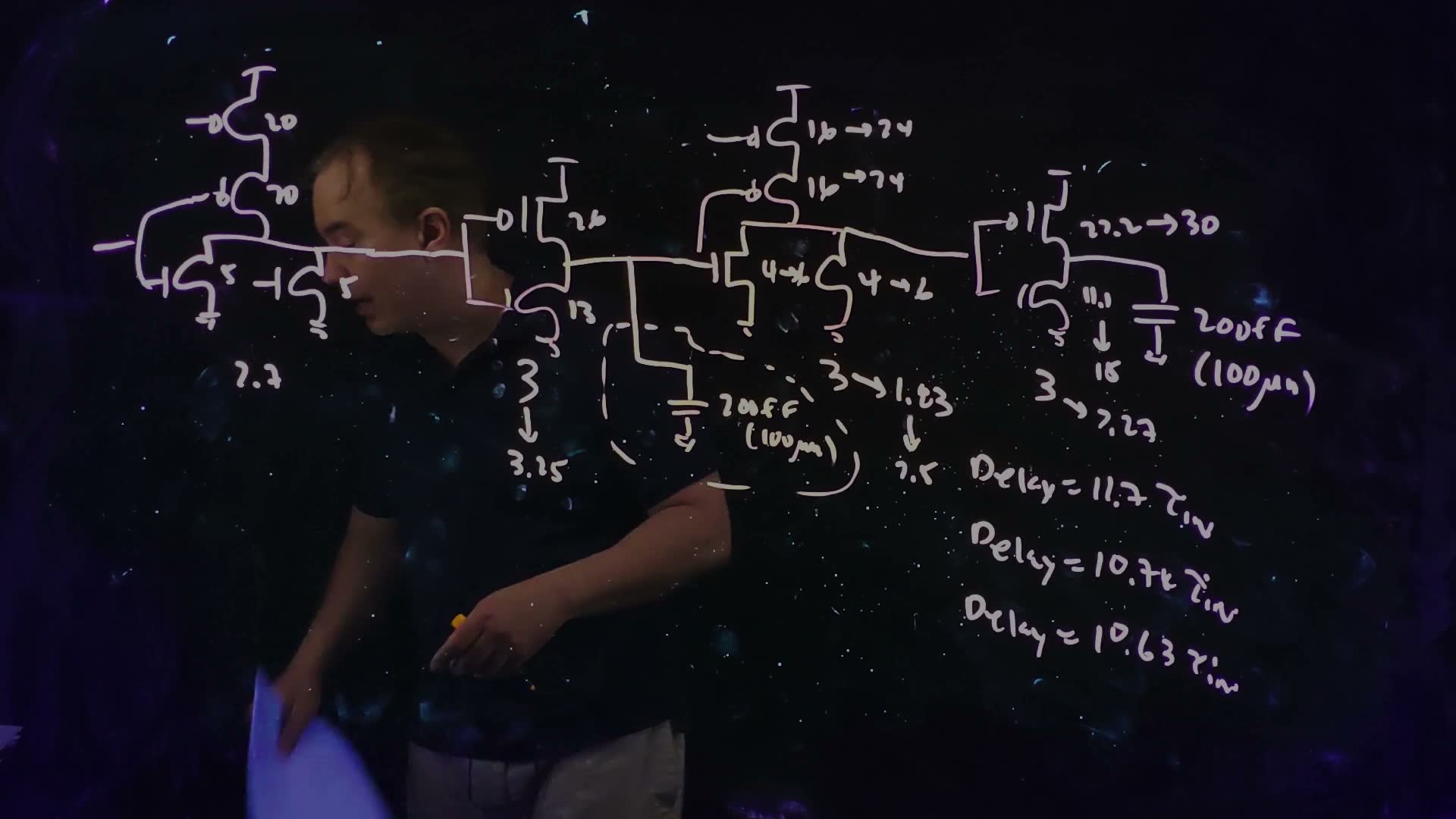
“Whenever I have a fan-out like this … I have the ability now to size this up, reducing its gain substantially without increasing the gain of this by very much … then if I created situations where the gains have become more unequal here, I can resize to balance those out” (54:22). That is the recipe. The lecture gives no exact method (54:22), and neither does this chapter; the widget shows how far it can go.
added The board’s gains 3.25 and 2.7 fit inverter 2 taken as 26.7/13.3 µm (input 40 µm, the size for a gain of exactly 3 on its 120 µm load: , ) rather than the 26/13 it writes, and its totals are sums of rounded gains: and . Either way the lesson is the same.
What to notice.
- Press the two steps in turn: the orange bar (the stage driving the branch) barely moves while the NOR’s bar collapses.
- Keep enlarging NOR 3: the delay keeps falling until about NFETs 9.3 µm (10.55 τ_inv), then rises again; “at some point it’s not going to work anymore” (53:19).
- The branching factor falls as NOR 3 grows, and with it : unlike Sections 2–7, is not a constant here.
- “Best” added lets every gate after the first move at once: 9.81 τ_inv, with inverter 2 grown to 34/17 µm. The best gains are not equal (3.43, 3.43, 1.48, 1.48): the two stages before the branch share one value, the two after it a smaller one.
- Set the branch to 0: , returns to , and “best” gives four equal gains, , as in Section 3.
Common mistakes.
- Equalizing all the gains anyway. With a branch, equal gains are no longer optimal.
- Resizing the stage that drives the branch so that its own gain is back to normal, and stopping there. Its input grows, so the gain moves to the stage before it; the total barely changes (MT17-5d’s trap; next check).
- Forgetting that resizing a gate changes its predecessor’s load: recompute both gains after every change.
Check yourself In the lecture's branch example (start sizes), make NOR 3's NFETs 8 µm (PFETs 32 µm) instead of 6. What are the new gains and delay? And with 12 µm?
8 µm: NOR 3’s input is 40 µm, normalized 24 µm. Inverter 2: ; NOR 3: ; the others 2.60 and 3.00. Total , better than the 6 µm step. 12 µm: inverter 2 , NOR 3 , total : worse again. The best single change is near 9.3 µm (10.55).
Check yourself A chain of four inverters has inputs 3, 12, 48 and 192 µm (the first fixed) and drives 768 µm: every gain is 4. A 96 µm branch is added at the second inverter's output. What is the delay? A designer resizes the second inverter so that its gain is 4 again. What is the delay now? What would help?
With the branch the second inverter drives : gain 12, total . Resizing it to gain 4 makes its input , so the first inverter’s gain becomes : still 24. The excess just moved one stage back. Better: balance the first two stages, input , gains 6.93 and 6.93, total . Letting the later gates grow too, as the lecture does, reaches about . (MT17-5d’s key falls into this trap.)
10. Stacks: why the bottom device is slow
The idea. The delay model describes the device at the top of a stack, nearest the output. A device lower down must first discharge the internal node above it before the output can move, and the penalty grows roughly as the square of the stack height.
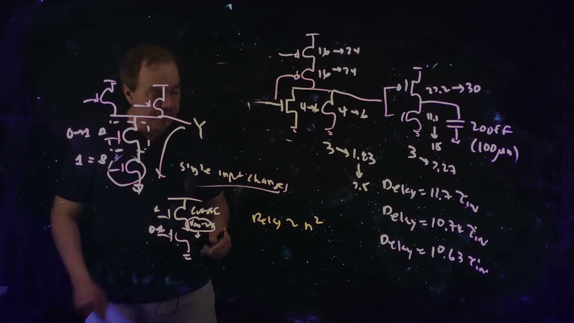
Everything so far assumes single input changes (55:44) board, and “all of this delay modelling … really only applies to the top device in the stack” (55:13). Take a NAND pulling its output Y down through its two NFETs.
Two ways to pull the NAND down (board, 55:57–58:33)
- B = 1, A switches 0 → 1 (A is the top device, nearest Y). The bottom device is already on; A turns on and discharges Y with its saturated current, then in triode. “That’s very similar to the inverter”: the delay model is accurate (56:17).
- A = 1, B switches 0 → 1 (B is the bottom device). Before the switch, the node between them was charged through A from the high output. An NFET stops conducting when its gate is only above its source, so the node sits near and A is cut off board (57:20).
- When B turns on it must first pull the internal node below . Only then does A turn on and start discharging Y (57:42).
- So the bottom device’s delay includes discharging the internal node first: it is slower.
The further down the stack, the slower: “that delay degradation of the bottom device on the stack will go something like the square of the height of the stack” (58:33) board, written Delay ∼ n². The lecture gives no derivation, and neither does this guide. That is why stacks are “yucky” (56:47): two is fine and unavoidable for complex functions, three deserves “a bit of an askance glance”, and beyond three you should break the gate up.
Back to Chapter 7. added This is the reason Lecture 7 promised (Chapter 7, pin swapping): the device nearest the output switches fastest, so a late-arriving signal should drive the input nearest the output. The early inputs have already set the lower devices, and the internal nodes are already discharged when the late signal arrives.
Check yourself A 4-input NAND has inputs A (nearest the output) to D (nearest ground). Three inputs are already 1 and the fourth rises. Which input gives the longest delay, and why? Which should get the latest signal?
D, at the bottom. With A, B and C at 1, the three internal nodes above D have been charged to about through the conducting devices, while D was off. When D rises it must discharge all three nodes before the output can fall; the penalty grows roughly as . The latest signal should go to A: with B, C and D already on, the nodes below A are already at ground and A switches like an inverter. (MT17-3d asks for this explanation.)
Check yourself Why does the internal node of the NAND sit near VDD − VT, and not at VDD, when A = 1 and B = 0?
It is charged through the top NFET from the output at . The NFET’s source is the internal node; as that node rises, the device’s gate-to-source voltage shrinks, and when it reaches the device turns off. The node stops near (Chapter 5’s body effect raises a little, so it stops slightly lower).
What comes next (59:06). Lecture 9 turns to layout: design rules and stick diagrams (Chapter 9).
On the exam
Path sizing is on every past paper: Question 5 of three midterms (MT23, MT21 and MT17: 40, 35 and 40 of 150 points) and one question on each of the four finals (20 to 35 points of 200 or 250). Each part below links its full solution; the exam-way twin and the path-sizing card exist so far for MT23-5.
| Section | Past-paper parts (points) | What they ask |
|---|---|---|
| §1 gain from the normalized inverter; §5 estimating a path | MT23-5a (10), MT17-5a (10), FN19-8a (10), FN10-9a (10), FN12-8a (15) | the delay of a path as drawn: every gain, then times their sum |
| §2 path delay and path effort; §3 equal gains; §6 resizing | MT23-5b (10), MT17-5b (10), MT21-5a (15), FN17-7a (8 or 10, illegible), FN19-8b (15), FN10-9b (14), FN12-8b (15); with Chapter 12, MT24-5c (20) | , , the widths sized back from the load, the new delay |
| §4 how many stages; §7 adding stages | HW3-3b (homework); M7 Question 5c (10, practice) | compare for the stage counts the logic allows |
| §8 branching effort | MT23-5c (10), MT17-5c (10), FN19-8c (10) | the delay with a side load at fixed sizes: only the gain of the stage driving that node changes |
| §9 retuning around a branch | MT23-5d (10), MT17-5d (10), MT21-5b (20), FN17-7b (12) | rebalance the overloaded pair, then trade the two sides of the branch |
| §10 stacks | MT17-3d (8) | why the bottom device of a stack is slow, and which input gets the late signal |
Memorize.
- Gain the load the normalized inverter’s input . With : , , . With equal strengths: . AOI22 and OAI22: either way.
- ; when nothing branches, when something does.
- and , when is fixed (no branch, and fixed).
- The best gain per stage is about , 3–4 in practice; about stages; add inverters in pairs, next to the load.
- . A branch makes depend on the sizes, and the best gains are then unequal.
- The bottom device of a stack is the slowest (Delay ); the latest signal goes to the input nearest the output.
Derive (each in about three lines).
- The gain from the normalized inverter. The gate pulls down like its normalized inverter’s NFET, , so its delay is . With that is : the load over the normalized input (Section 1).
- Equal gains. Two stages: ; the derivative is zero at ; for stages each neighbouring pair keeps a fixed product when the gate between them is resized, so all gains are equal (Section 3).
- The best gain per stage. , so ; the derivative of is zero at , (Section 4).
- Sizing back from the load. The last stage’s normalized NFET is ; double each device that sits in a stack of two; the result is the next stage’s load (Section 6).
Method card. Every path-sizing question follows the path-sizing card of the playbook: recognize the picture, tabulate the stages, then (a) the delay as drawn, (b) equal gains sized back from the load, (c) the side load on one stage, (d) a retuning by pairs.
Formulas to remember
| Formula | Meaning |
|---|---|
| gain | the normalized inverter has the gate’s drive; input ( for equal strengths) |
| path delay: sum of the gains | |
| , , | path effort; constant if , fixed and nothing branches |
| , | equal gains minimize the delay |
| , best | stage count; 3–4 per stage in practice (drain cap); ; add inverters in pairs |
| size back from the load: , then double stacked devices | equal-gain sizing; the first gate stays fixed |
| added inverters next to the load | same delay, less total width and dynamic power |
| , | branching effort; depends on the sizes, so is not fixed |
| enlarge the gate after a heavy branch, then rebalance | retuning around fan-out; equal gains are no longer optimal |
| bottom of a stack: Delay ∼ | internal nodes at must discharge first; late signal on top |
The lecture’s boards