11. Dynamic and domino logic
Static CMOS gives the right answer whatever its sizes, but it pays for that with a PFET for every NFET: extra input capacitance on every gate. Ratioed logic (Chapter 10) drops the PFETs and pays with static current. Lecture 11 finishes those two families, then builds a third: dynamic logic, in which the output node is charged up on one phase of a clock and conditionally discharged on the other. It is fast, because the evaluation is done by NFETs alone and fights nothing. But its output node is connected to nothing for part of the time, and the second half of the lecture is a tour of everything that can disturb a node like that, and of the circuits that protect it.
After this chapter you can:
- state the two problems of ratioed logic and why IDDQ testing needs its pull-ups switched off;
- size a complementary pass transistor together with its driving inverter, using the lecture’s R, 2R, 4R model;
- explain precharge and evaluate, the dynamic node, the collision and the footer that prevents it, and read the function of a dynamic gate;
- explain the race between two cascaded dynamic gates, and how the inverter of domino logic removes it; say why domino logic is non-inverting and why it is fast;
- compute the evaluate delay of a footed dynamic stack with the delay model of Chapter 7;
- explain leakage, charge-sharing, coupling and power-supply noise on a dynamic node, and size a half latch by the one-tenth rule;
- estimate a charge-sharing droop and name the babysit devices that prevent it.
Boxes and equations marked board were written in the lecture. Parts marked added are explanations or examples this guide adds.
Before you start
You need these ideas from earlier chapters. Each is restated here.
- Static, ratioed, dynamic (Chapter 7). A static CMOS gate has a pull-up network of PFETs and a pull-down network of NFETs, and for any settled inputs exactly one of them is on. Both on is ratioed logic; neither on is dynamic logic.
- The delay model (Chapter 7). A transistor of width is a “resistance” , with and in kΩ·µm; a gate input is per µm of width; delay . Devices in series add: a stack of needs each device times wider for the strength of one. (or when a problem says the NFET and PFET have equal strength).
- Pass transistors and the half latch (Chapter 10). An NFET passes a good 0 but a high only up to ; a PFET passes a good 1 but a low only down to . A complementary pass transistor puts one of each in parallel, driven by complementary signals. A half latch is a weak PFET wrapped around an inverter that pulls a degraded high up to . Transistors connected through their sources and drains form one channel-connected component (CCC).
- Pseudo-NMOS (Chapter 10). A PFET with its gate grounded as an always-on load over an NFET pull-down network.
- Noise margins and the switching threshold (Chapter 6). An inverter with a stronger PFET switches at a higher input voltage.
- Subthreshold leakage (Chapter 4). An NFET with its gate at 0 still conducts a small current.
Notation. Sizes such as “4/2” mean a PFET 4 µm wide and an NFET 2 µm wide, as in Chapter 7. “clk” is the clock; its complement. The board first calls the dynamic node Y (17:08); once the lecture adds an inverter after it, this chapter calls the dynamic node X and the inverter’s output Y.
1. Ratioed logic, its two problems and IDDQ testing
The idea. Pseudo-NMOS makes wide NORs cheap, but its low output is never quite at ground and it burns power whenever its output is low.
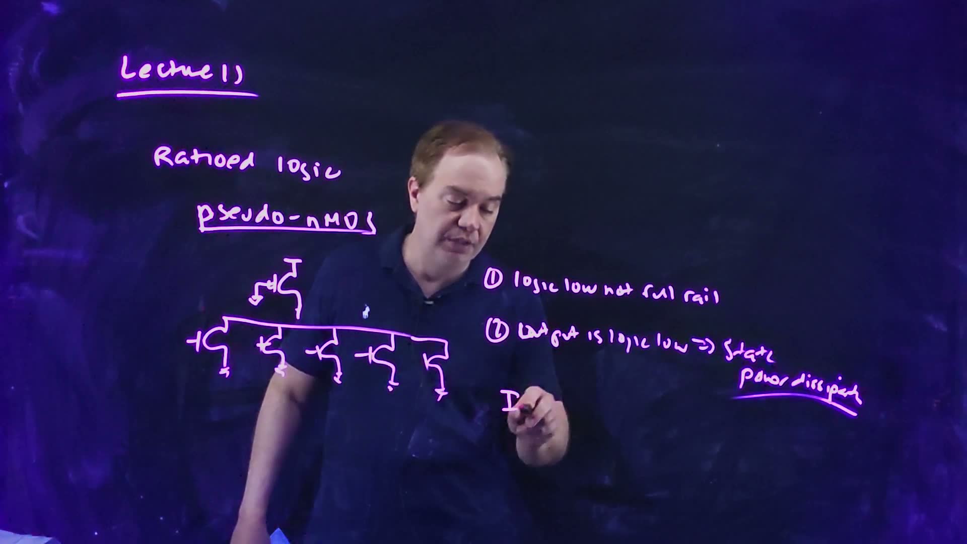
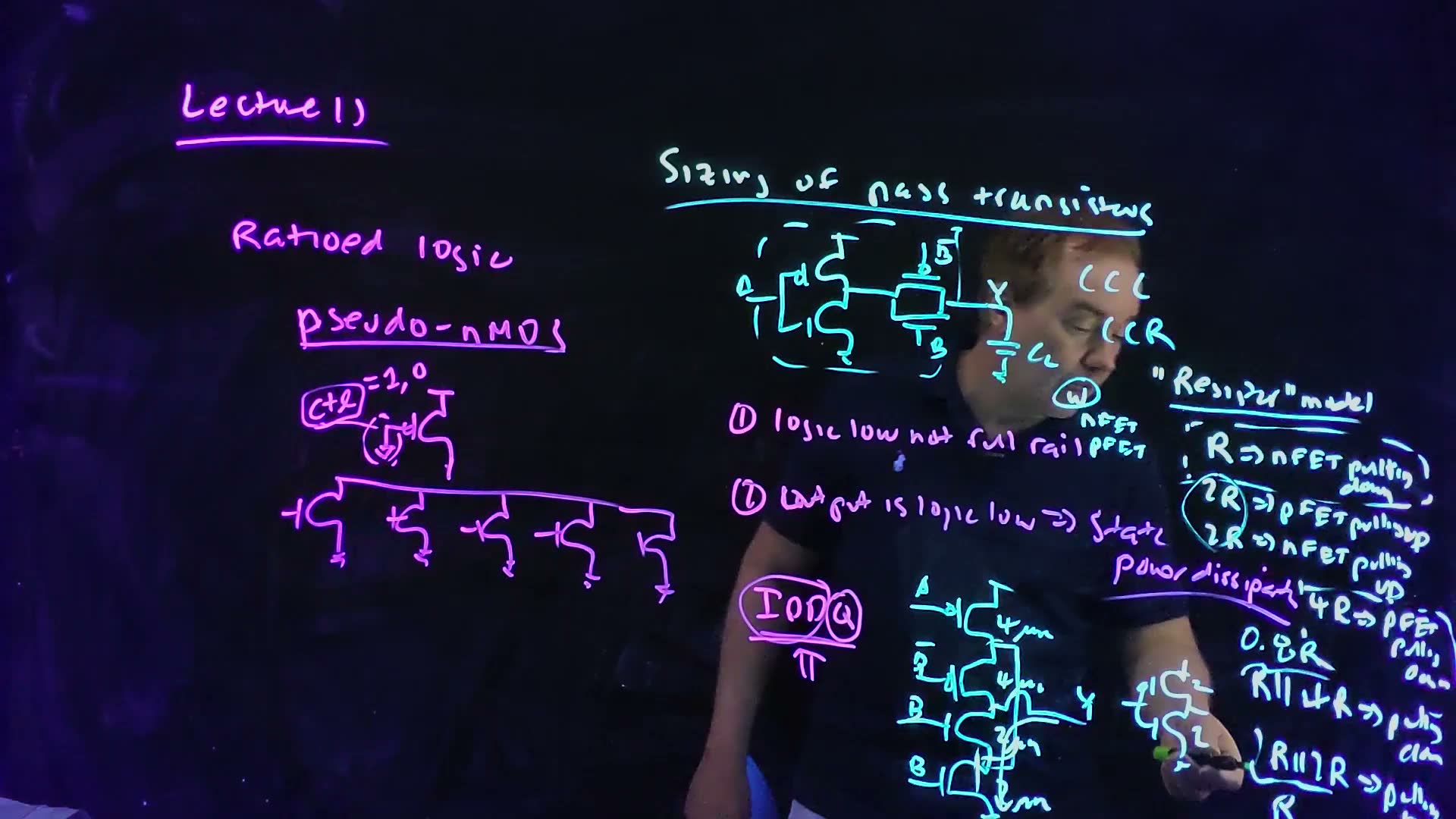
The lecture opens where Lecture 10 stopped (00:05). The commonest ratioed gate is pseudo-NMOS, inspired by the old NMOS logic with its depletion-mode load: in CMOS, the load becomes a PFET with its gate tied to ground (00:15). Its strength is the wide NOR: any number of parallel NFETs, with no stack of PFETs to carry along (00:44).
Two problems (00:57–01:39) board:
- The logic low is not full rail. With the output low, the PFET load is still on, fighting the pull-down. added The output settles where the two currents balance, a little above ground. The NFET/PFET strength ratio must make it low enough that the next gate doesn’t misread it.
- Static power. Whenever the output is low, current flows from to ground through both devices, all the time.
It is still worth it for very wide ORs; programmable logic arrays (PLAs), a NOR followed by a NOR, use it (01:39).
IDDQ testing (02:11) board. When a chip comes back from fabrication, one test measures the quiescent supply current, (the Q). A power-to-ground short anywhere on the chip shows up as a large quiescent current. Ratioed logic draws static current by design and would hide such a short, so its load’s gate is not tied to ground but to a control line: 0 in normal operation (load on), 1 in test mode (load off) (02:33–03:11). The board writes it as “ctl = 1, 0” on the PFET’s gate (10:53). Testing comes back later in the course.
Check yourself A pseudo-NMOS NOR has eight inputs. In normal operation, for which input combinations does it draw static current? Why would that spoil an IDDQ test, and what does the control line do?
It draws current whenever its output is low, that is, whenever at least one input is 1 (255 of the 256 combinations): the PFET load and the conducting NFETs form a path from to ground. An test looks for unexpected quiescent current, so these legitimate currents would mask a short. Setting the control line to 1 in test mode turns the load PFET off, and the gate draws nothing.
2. Sizing pass transistors
The idea. A pass transistor is sized together with the gate that drives it. Because both devices of a complementary pass transistor help on both edges, its PFET needs to be only as wide as its NFET.
Size it with its driver
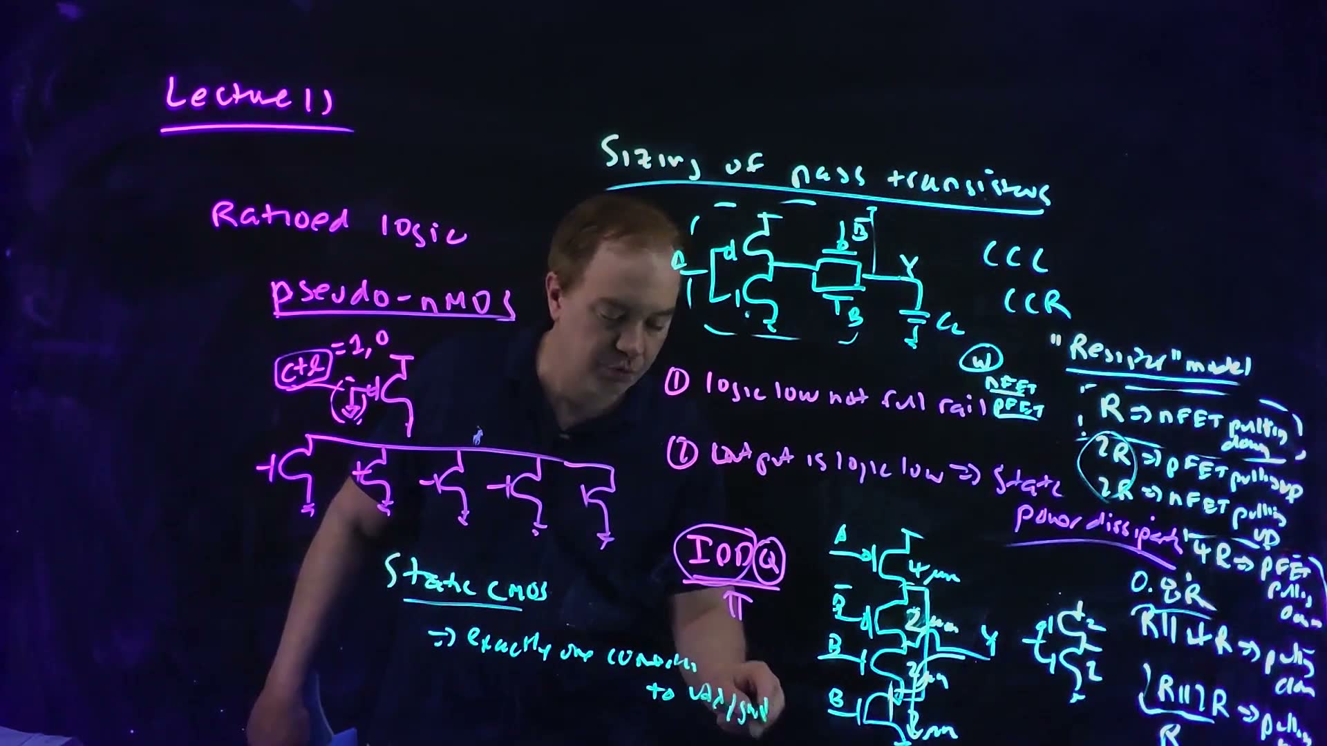
“Just as delay makes no sense if we don’t consider the driving gate, sizing of pass transistors makes no sense unless we consider the driving gate” (03:43). The simplest case: an inverter (input A) drives a complementary pass transistor (gates B and ), which drives a load board. Together they are one channel-connected component (CCC, or region, CCR): current flows from the supply through both.
Redraw it (04:14–04:51) board: from , the inverter’s PFET (A) in series with the pass PFET () reaches the output Y; from Y, the pass NFET (B) in series with the inverter’s NFET (A) reaches ground. It is a two-high PFET stack and a two-high NFET stack. (The board labels the bottom NFET “B”; it is the inverter’s NFET, driven by A.)
For the drive of a 2/1 inverter, Chapter 7’s stack rule gives the first attempt (05:00): NFETs 2 µm each, PFETs 4 µm each board.
Both devices help on both edges
The catch (05:18–06:45): when the output is pulled down, current flows through the pass NFET and through the pass PFET; when it is pulled up, through the pass PFET and the NFET. Only the PFET can pull all the way to , and only the NFET all the way to ground; the other one keeps losing overdrive as the output moves and finally cuts off (at for the NFET, at for the PFET). That is why the complementary pass transistor was used in the first place. But during most of each transition, both help.
The resistor model
For equal widths , “without proving it” (07:13–08:42) board:
| device and edge | resistance |
|---|---|
| NFET pulling down (its good direction) | |
| PFET pulling up (its good direction) | |
| NFET pulling up (losing overdrive) | about |
| PFET pulling down (losing overdrive) | about |
The weak direction is about twice the good one, because the device keeps losing overdrive while it works (08:42).
Pull-down and pull-up of the pass transistor (board, 08:42–09:26)
- Pulling down, the NFET and the PFET are in parallel board: . (The lecturer first says “like 0.9R”, then corrects himself.)
- Pulling up board: .
- These are roughly equal, and both are about the NFET’s own (09:26).
- So the pass transistor at equal widths acts like its NFET alone, in both directions. Its PFET doesn’t need the usual factor of two: size the pass PFET equal to the pass NFET, 2 µm rather than 4 µm (09:37) board.
The rule of thumb (09:52): size the stack as you normally would, then make the pass PFET equal to the pass NFET, always with the driving gate in view. Compare the 09:27 frame in the gallery, where the pass PFET is still 4 µm, with 10:53, where it has become 2 µm.
Worked example. added The lecture’s circuit: inverter 4/2, pass transistor 2/2. Resistances in units of (kΩ·µm) divided by µm.
- Target: each element of a two-high stack should be half the 2/1 inverter’s resistance, .
- Inverter NFET: . Inverter PFET: . On target.
- Pass transistor down: NFET , PFET ; in parallel .
- Pass transistor up: NFET , PFET ; in parallel . On target.
- Whole path: down , up , against the 2/1 inverter’s both ways.
- With a 4 µm pass PFET instead: down , up , so both ways: faster than needed, and 2 µm more gate on the line.
Common mistakes.
- Copying the inverter’s 2:1 ratio into the pass transistor. The PFET’s job on the rising edge is shared with the NFET.
- Sizing the pass transistor alone. Its resistance is in series with the driver’s; the two are one stack.
- Forgetting that the weak device stops helping near the rail. The 0.8R and R are averages over a transition, a rough model the lecturer offers “without proving it”.
Check yourself With Rnfet = 2 kΩ·µm and Rpfet = 2Rnfet, the lecture's 4/2 inverter drives 30 fF through a 2/2 µm complementary pass transistor. Estimate the falling and the rising delay at the output.
Falling: the path is , so . Rising: , so . A 2/1 inverter driving 30 fF directly would take both ways.
Check yourself An NFET-only pass transistor of width W is driven by an inverter. Using the lecture's table, how strong is it pulling up compared with pulling down? What does Chapter 10 add to that?
Pulling down it is ; pulling up about , twice as slow, because it loses overdrive as the output rises. And it never finishes: it cuts off at (Chapter 10), which is why the complementary pass transistor or a half latch is used.
3. Why dynamic logic
The idea. Static CMOS is robust but carries a PFET network; pseudo-NMOS drops the PFETs but fights its load all the time. Dynamic logic keeps the first advantage of each.

Static CMOS: exactly one connection from the output to or ground (10:36) board. Connected to both: ratioed logic. Connected to neither: a high-impedance node, and that is dynamic logic (11:03). The lecturer believes it was invented at Bell Labs, by people inspired by NMOS design (11:41), and follows their reasoning.
The complementary static NOR (12:15–13:40):
- it always gets the right answer, however it is sized (“very, very hard to break”); it draws no static power;
- but while it switches, both networks are briefly on: crowbar current that doesn’t charge the load, burning power and slowing the gate (Chapter 6);
- and it carries the PFET switches, extra capacitance for the preceding gate to drive. That is exactly what raises the logical effort of complex gates (Chapter 7).
Pseudo-NMOS (13:40–14:39) removes the PFET capacitance, but turns the brief crowbar current into a permanent fight with its load. “Is there a way to get the best of both worlds?” (14:39): no PFET network, and no fight.
4. Precharge and evaluate
The idea. Put the pull-up PFET’s gate on a clock. On one phase it charges the output high (precharge); on the other it is off, and the NFET network either discharges the output or leaves it floating at its precharged 1 (evaluate).
The two phases
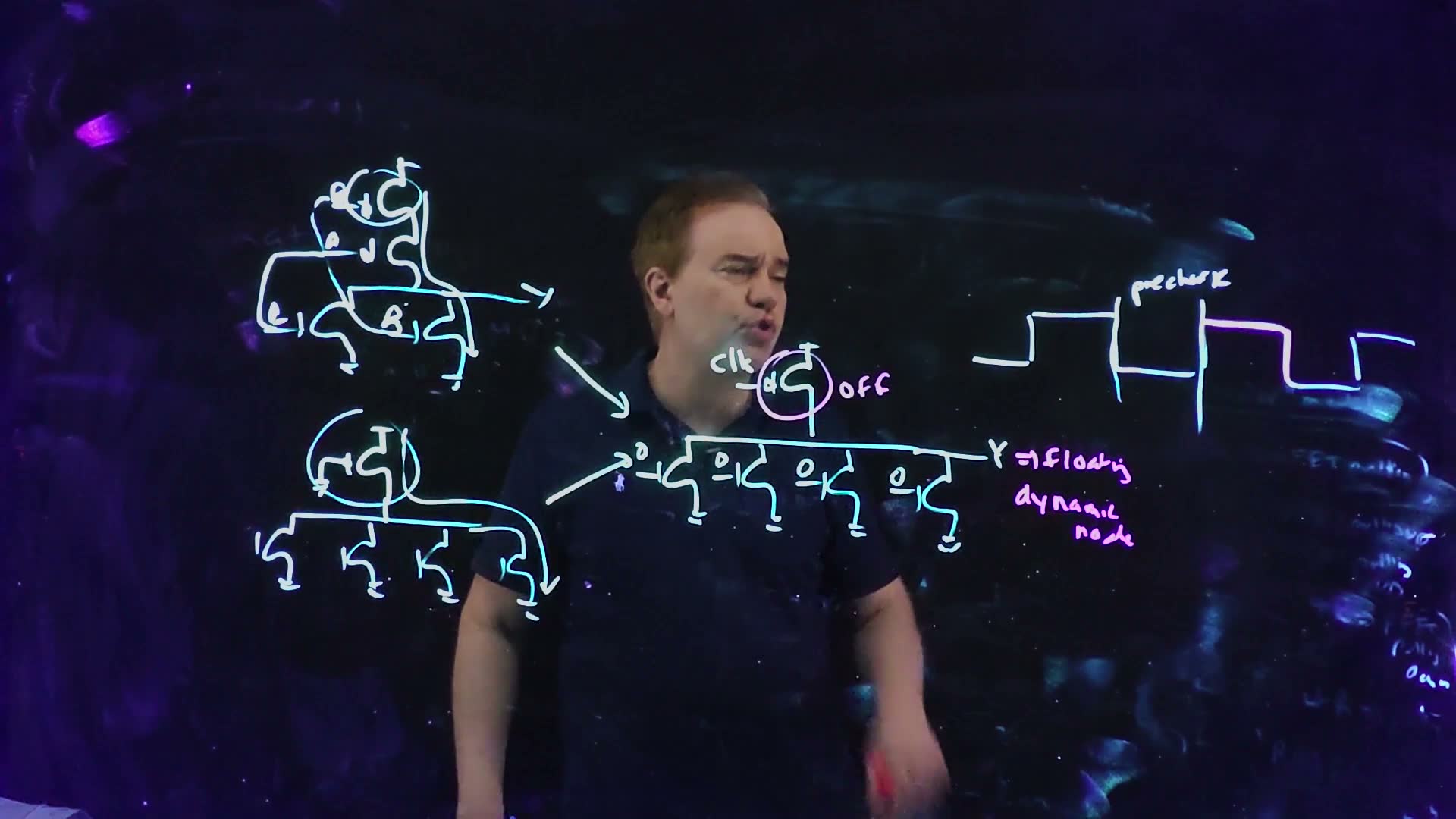
Keep pseudo-NMOS’s NFET pull-down network (again, a wide NOR is natural here), and tie the PFET’s gate to a clock that toggles between 0 and 1 (15:07–15:49) board:
- clk = 0: precharge. The PFET is on and pulls the output Y all the way to (15:59).
- clk = 1: evaluate. The PFET is off (16:12). If every input is 0, nothing connects Y to or to ground: Y is floating, in a high-impedance state, a dynamic node board (16:35). It stays at 1 only because its capacitance was charged to : the logic value is stored as charge (16:53).
- If any input is 1 during evaluate, Y is pulled down to 0 (17:51). With inputs A, B, C, D the gate computes : a NOR (17:27).
The next precharge pulls Y back to 1, and the cycle repeats.
The collision and the footer
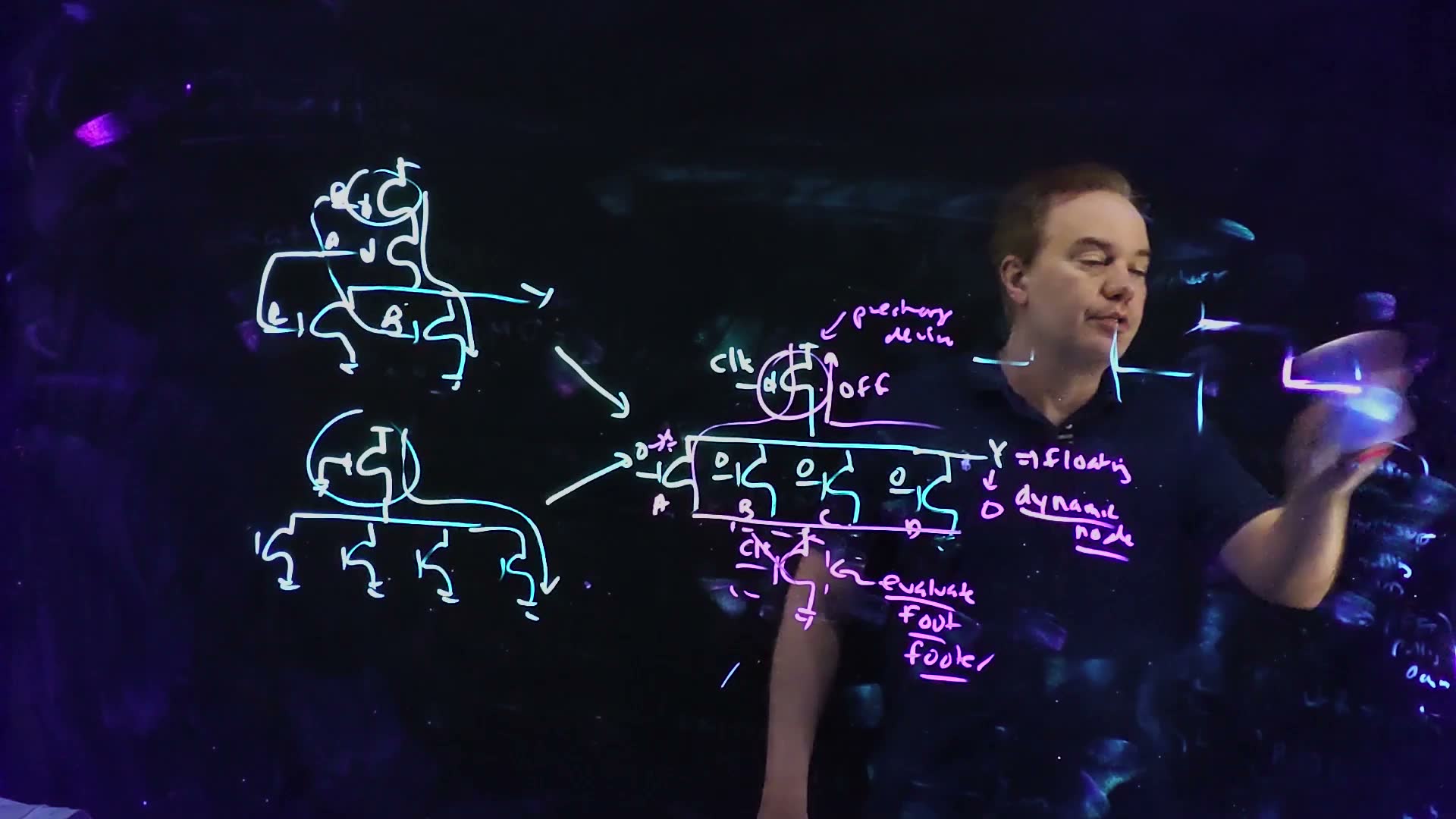
What if an input is still 1 when the clock goes back to 0 (18:18)? The PFET precharges while the NFET pulls down: a collision, with short-circuit current through both. The usual fix is one more NFET at the foot of the network, also driven by the clock (18:43) board. It is called the evaluate transistor, the foot device or the footer; the clocked PFET is the precharge device (18:57–19:06).
During precharge the footer is off, so the pull-down can never conduct, whatever its inputs (19:12). The price is delay: the footer adds one device to the stack (19:40). It can be left out in circuits that guarantee every input is back at 0 before the next precharge begins (19:40–20:06); the lecture returns to that later (Chapter 12).
What to notice.
- In evaluate with all inputs 0, X is 1 with every device around it off: the “floating” rows of the log.
- Raise an input in evaluate and X falls; lower it again and X stays 0. A dynamic gate can only discharge during evaluate: an input that rises by mistake, even briefly, does damage that the next precharge alone repairs.
- Remove the footer and return to precharge with an input at 1: collision.
Reading the function of a dynamic gate
added In evaluate, the dynamic node is 0 exactly when the pull-down network conducts. So the node computes the complement of the network’s switching function , like a static gate: series NFETs are AND, parallel ones OR, and . An inverter after it gives itself (Section 6).
The evaluate delay
added Precharge happens for every gate at once and is not on the critical path (Section 7); what matters is the evaluate delay, the time to discharge the node through the network and the footer, in series. Chapter 7’s model applies directly.
A footed stack (added)
- A dynamic gate’s pull-down is A and B in series with the footer, each NFET 4 µm; the load is 50 fF; .
- Three 4 µm devices in series act as one NFET of (Chapter 7’s stack rule).
- 50 fF is of gate. Delay .
- With : . If the problem says the NFET and PFET have equal strength, and the delay is .
- The 1 µm precharge PFET doesn’t appear: it is off during evaluate. Without the footer, the stack would be wide and the delay : the footer costs 50% here.
Common mistakes.
- Leaving the footer out of the evaluate stack. It is in series with the network and must be counted.
- Counting the precharge device in the evaluate delay. It is off.
- Calling a footed gate’s output “static” because it is driven during precharge. During evaluate with the network off, nothing drives it.
Check yourself A dynamic gate's pull-down network is A in series with (B in parallel with C), above a footer. What does the dynamic node compute in evaluate? What does an inverter after it give?
The network conducts when is true, so the node is and the inverter’s output is . (Reading the function of a dynamic stage is MT24-5a’s first step; its stages are this kind of gate, one of them in Lecture 12’s p-type form.)
Check yourself In MT17-3c, a dynamic gate has a 1 µm clocked PFET and three 4 µm NFETs in series (A, B and the clocked footer), driving 50 fF with Cg = 2 fF/µm. The NFET and PFET have equal strength. Find the A-rising-to-Y-falling delay in evaluate, with B = 1, in units of τinv.
The stack acts as one NFET; 50 fF is 25 µm of gate. With equal strengths the FO1 inverter is W/W, so . Delay . (This is MT17-3c; its key’s 9.375 τinv is right.)
Check yourself Why can't a footless dynamic gate accept an input that is still 1 when the clock falls?
With clk = 0 the precharge PFET is on; an input at 1 turns the pull-down on as well, and with no footer the two fight: a collision, with current from VDD to ground and an output somewhere in between (18:18). A footless gate is safe only if its inputs are guaranteed to be 0 before precharge starts.
5. Cascading dynamic gates: the race
The idea. A dynamic gate’s output is 1 during precharge. Fed straight into the next dynamic gate, that 1 starts discharging the next gate before the first has decided; which of two delays wins then decides the answer.
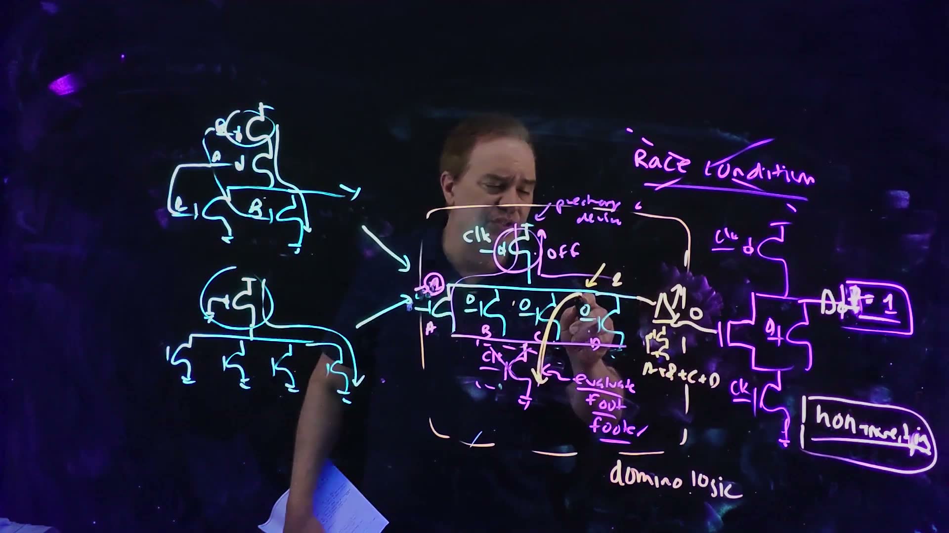
Cascading is unavoidable: one NOR must drive another (20:21) board. Take two dynamic NORs on the same clock, the first’s output Y driving one input of the second, every other input of the second at 0 (20:47–21:32):
- Precharge. Both outputs go to 1 (21:32).
- Evaluate. Input A of the first gate is 1, so the first output should fall to 0, and the second gate, whose inputs are then all 0, should stay at 1 (21:12).
- But the first gate takes a finite time to discharge. Until it does, its output is still 1, and that 1 is turning on the second gate’s NFET, which starts discharging the second output (22:09–22:36).
- If the first gate falls fast, the second output loses little and stays a 1. If the second output falls fast, it reaches 0 before the first gate has turned its NFET off, and stays 0, the wrong answer: once discharged, a dynamic node can’t recover (23:02).
The answer depends on which of two delays is faster: a race condition board (23:29). Race conditions are “very, very bad”: the delays can’t be controlled precisely, and they change with process, voltage and temperature (23:40). A few designs use a race on purpose, carefully controlled and margined across all corners; this one is uncontrolled (24:08–24:38).
What to notice.
- With a wire between the stages and A = 1, slide τ1/τ2 past 1: stage 2 ends below VDD/2 and is read as 0.
- Even when stage 1 wins (τ1/τ2 = 0.5), stage 2 has lost about 30% of its charge: it is left with less margin against the noise of Sections 8–12.
- With the inverter, every ratio gives the right answer.
Check yourself In the toy model of the widget, stage 2 keeps 2−τ1/τ2 of its charge. With τ1 = 0.5τ2 and τ1 = 2τ2, what does it end at, and how does its inverter read it? Why is a design that works at τ1 = 0.5τ2 still a bad design?
, read as 1; , read as 0. The first case works only because of a delay ratio that varies with process, voltage and temperature (23:40); a slow corner for stage 1 or a fast one for stage 2 flips it. And even when it works, the node has lost charge that noise can finish off.
6. Domino logic
The idea. Put an inverter after every dynamic gate. During precharge every inverter output is 0, so no gate can start discharging the next one before it has evaluated.
The race exists because a precharged output is a 1 (24:38). If it were a 0 during precharge, the next gate would be off until the previous one had decided. So insert an inverter between the stages (25:06) board. The dynamic gate and its inverter together are domino logic (25:36) board.
Why “domino” (25:51). Precharge stands every domino up. Evaluate pushes the first one; each one either stays standing (a 1 on its dynamic node) or falls, and a falling one can knock over the next. At the end of the cycle, precharge stands them all up again.
Non-inverting (26:18) board. With the inverter, each stage computes the network’s function itself: the NOR becomes board, an OR. Non-inverting logic is not logically complete: no network of ANDs and ORs makes an inversion. The remedies (27:12–27:56): push the inversions back into the latches that feed the logic and carry both the true and the complement of each signal through the logic as needed, or push them forward to some static logic at the end. Both come up again with latches and clocking, after the midterm material.
Worked example. added With true and complement signals available, a domino gate can make an XOR: a pull-down of A in series with , in parallel with in series with B. The network conducts when , so the dynamic node is and the domino output is .
Check yourself Why can't a chain of domino gates fed only by true signals compute the NAND of two inputs?
Every domino stage computes the AND–OR function of its network on its inputs, which is non-inverting: if an input rises, the output can only rise or stay. NAND falls when its inputs rise. It needs or from somewhere else (a latch that supplies complements, 27:12): with them, is an OR.
Check yourself A domino gate's network is (A in series with B) in parallel with (Ā in series with B̄). What do the dynamic node and the output compute? MT23-3a asks the same of a gate built the other way up (Chapter 12's p-type form: PFETs evaluate and pull a node that rests at 0 up to 1). Its PFETs conduct when (A = 0 or B̄ = 0) and (Ā = 0 or B = 0). What is its output after the inverter?
Here the network conducts for (A and B equal), so the node is and the output is the XNOR. In the exam’s gate, the PFET network conducts when ; there the node rises when the network conducts, so the node is the XNOR and the inverter gives , an XOR. Always ask which way the node moves when the network conducts.
7. Why domino is fast: a skewed logic family
The idea. All the logic is done by NFETs on one edge, against nothing; the other edge, the precharge, happens everywhere at once. So each device can be sized for the edge that matters.
Why go to all this trouble (27:56)?
- Only NFETs evaluate. The logic no longer carries PFETs, the original motivation, as with pseudo-NMOS (28:13).
- Nothing to fight. When the pull-down discharges the dynamic node, no PFET is trying to hold it up: the node is high-impedance, and “all I have to do is discharge the capacitor” (28:39). The evaluation is very fast. The next lecture puts numbers on it with logical effort and gain-based tuning (29:06; Chapter 12).
- One edge. All the logically important transitions happen on one edge: the dynamic node falling, the inverter’s output rising (29:06). The other edge is the precharge, which “doesn’t have any logically important evaluations on it” and happens in parallel for every gate.
So domino is a skewed logic family (29:33): each network is sized for the edge that carries the logic, and the other side is made small. In particular, the inverter after the dynamic node is not sized 2:1. Its PFET, which drives the rising output, is made much stronger than its NFET, which only resets the output during precharge, and “I have plenty of time to do precharge” (29:47–30:12).
added The skew has a price (Chapter 6). An inverter with a strong PFET switches at a higher input voltage, so the dynamic node, which sits at , needs to sag less before the inverter flips: its high noise margin shrinks. That matters for everything in the rest of this chapter.
Check yourself Why is the domino inverter skewed toward a strong PFET and not a strong NFET? What does that do to its noise margins, and which margin matters for the dynamic node?
Its output carries the logic when it rises (the dynamic node falling, 29:06); its falling edge is the precharge reset, which has time to spare. So the PFET is made strong. That raises the inverter’s switching threshold: grows and shrinks. The dynamic node rests at 1 and noise pulls it down, so the shrinking is the one that hurts. (MT23-3c asks the mirror question for a p-type gate, whose inverter has the strong NFET: there the small margin is .)
8. Leakage noise and the half latch
The idea. A node held only by its charge loses that charge through every off transistor attached to it. A weak PFET, driven back from the inverter, replaces it.
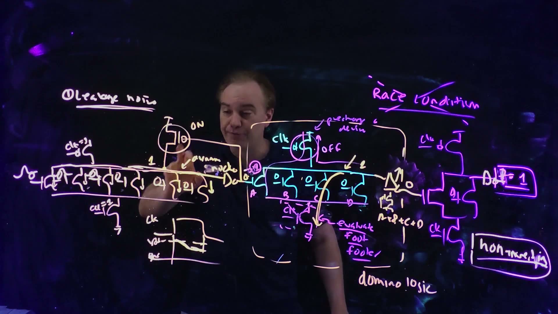
The dynamic node is fast precisely because nothing holds it, and for the same reason it is “very noise sensitive” (30:40). The lecture takes four noise sources in turn; dynamic gates are good for this, being “especially sensitive to all of them” (52:18).
Leakage noise
Take a very wide OR, natural in dynamic logic because width costs no PFET stack (31:58), in evaluate with all its inputs 0 (32:32) board. Each NFET is off, but each still conducts a little subthreshold leakage (32:43; Chapter 4). Together they slowly discharge the dynamic node: by the end of the evaluate phase it has drooped from by some amount, and if that is too much, the inverter flips and the gate falsely evaluates (33:22) board. Noise on the inputs makes it worse: a coupled blip that turns some of the NFETs on a little drains the node faster (33:39).
added The droop grows with the number of parallel devices and with the length of the evaluate phase, so a wide gate on a slow clock is the worst case.
The half latch
The fix (34:08) is the half latch already met with pass transistors (Chapter 10): a PFET from to the dynamic node, its gate driven by the domino inverter’s output board. While the node is 1, the inverter’s output is 0, the PFET is on, and it holds the node at 1 against leakage and noise (34:32–34:48). Strictly, the node is no longer dynamic (34:32).
It isn’t free (35:15): when the network should discharge the node, it must now fight the half latch until the inverter switches and turns it off. So the half latch’s size is a direct trade-off (35:15–36:00):
- weaker: faster evaluation, worse noise margins; none at all is the fastest and the noisiest;
- stronger: better noise margins, slower evaluation.
added The fight is also why a node with a half latch is not plain static CMOS either: correct operation now depends on the pull-down being stronger than the half latch, a ratio (the point of MT24-3a’s grading note about half latches in a pass-transistor circuit).
Common mistakes.
- Driving the half latch’s gate from the dynamic node. It is driven from the inverter’s output, so that it turns off once the node falls.
- Making it as strong as the pull-down. Then a real evaluation may never win the fight.
Check yourself MT23-3d asks how one transistor can improve the noise margin of a domino gate's dynamic node. What is it for the lecture's n-type gate, and how is it connected? What is the mirror device for a p-type gate whose dynamic node rests at 0?
A half latch: a weak PFET from VDD to the dynamic node, its gate on the inverter’s output, so that it is on while the node is 1 (34:08). For a p-type gate whose node is pre-discharged to 0 and pulled up by noise, the mirror is a weak NFET from the node to ground, gated by the inverter’s output, on while the node is 0.
9. Sizing the half latch
The idea. Make the half latch about one tenth as strong as the pull-down network. When minimum width is still too strong, add a series device and lengthen that one, not the one the output drives.

The rule of thumb (36:37) board: size the half latch to one tenth the strength of the pull-down network. It must be a weak device. How do you make one (37:11)?
- Reduce its width board. Until you reach the minimum width.
- Increase its length board: a longer channel conducts less (Chapter 4: current goes as ). But its gate area grows with , and that gate is driven by the inverter’s output: a direct extra load on the logic path, slowing the evaluation (37:11–37:42).
- Use a series device (37:42–38:38) board. Keep the device whose gate is driven by the output at minimum length and minimum width, and put a second PFET in series with it. The series connection already halves the strength, and the second device’s length can be increased as much as needed, because its gate doesn’t load the output. Strength ratios of about a tenth become reachable.
Worked example. added (From the Fall 2026 recitation.) A pull-down network of three NFETs in series, each 3 µm.
- The stack acts as one NFET of .
- One tenth of its strength: an NFET of .
- A PFET has half an NFET’s strength at the same width, so the half latch is a PFET of .
- That is narrower than any real minimum width: hence the series device, or a longer channel, of step 3 above.
Check yourself A domino gate's pull-down is one 2 µm NFET above a 2 µm footer. By the one-tenth rule, how wide should the half-latch PFET be (Rpfet = 2Rnfet)? If the minimum width is 0.5 µm, what does a second minimum-width PFET in series give?
The stack acts as a 1 µm NFET; one tenth is a 0.1 µm NFET, so a 0.2 µm PFET. A single 0.5 µm PFET would be 2.5 times too strong. Two 0.5 µm PFETs in series act as one 0.25 µm PFET, still 1.25 times too strong, so the series device is also lengthened (it doesn’t load the output). The one-tenth rule is a starting point, not a hard limit (36:37).
10. Charge-sharing noise and babysit devices
The idea. Internal nodes of the pull-down network that were left at 0 can steal charge from the dynamic node when a device above them turns on, even though no path to ground exists.
The mechanism
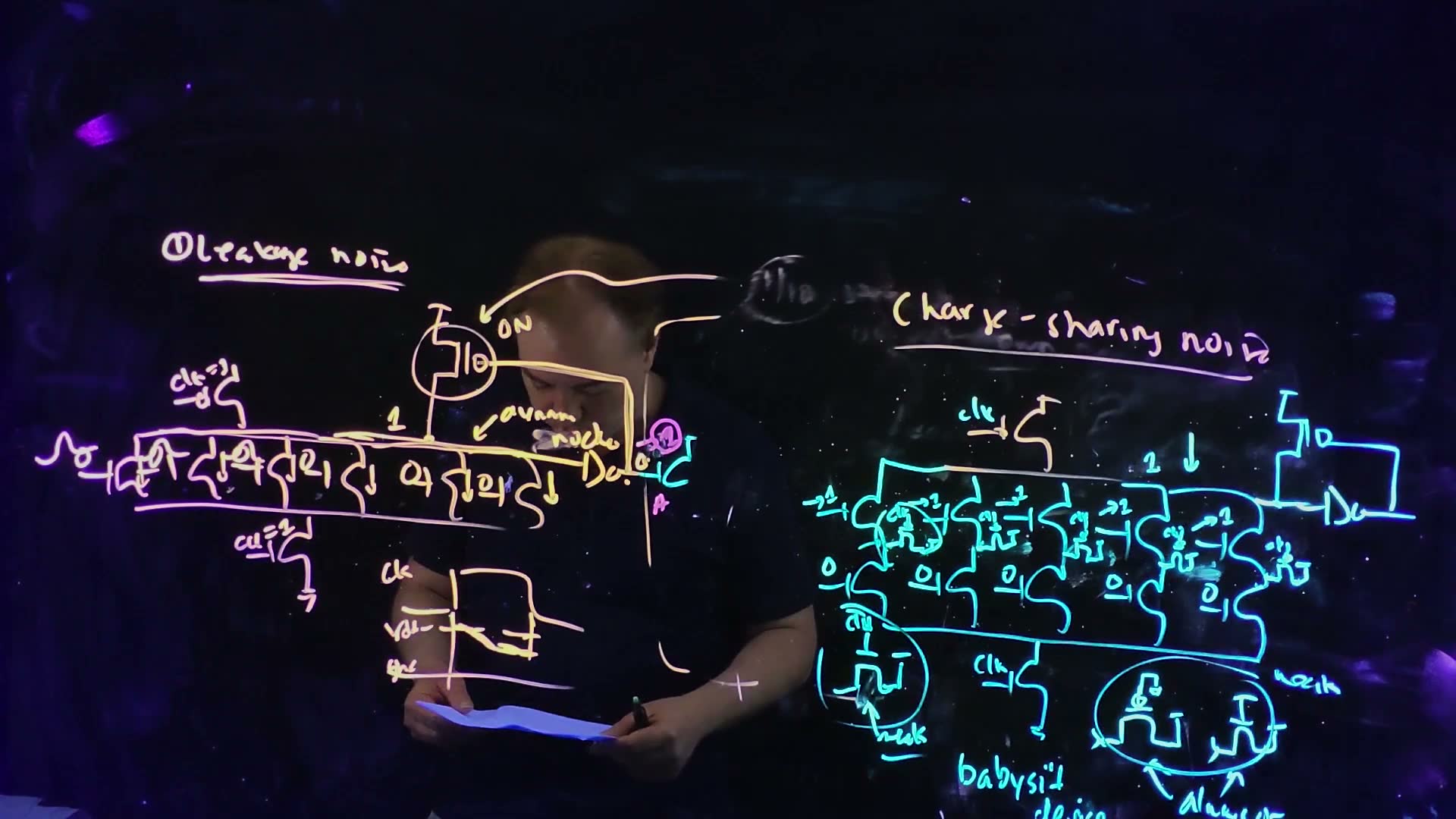
Take a wide AND-OR gate: several branches in parallel, each two NFETs in series (39:57–40:29) board. Suppose that in the previous cycle the lower NFETs were all on, so the internal nodes between the two devices of each branch were discharged to ground (40:59–41:23). Now, in evaluate, the upper inputs switch to 1 and the lower ones stay at 0 (40:41) board. No branch conducts to ground, so the dynamic node should stay at 1.
But each upper NFET now connects the dynamic node’s capacitance to an empty internal node. The charge on the dynamic node “gets shared across these capacitors” until they all reach the same potential (41:26), and the dynamic node’s voltage drops (42:00). If it drops far enough, the gate falsely evaluates. This is charge-sharing (or charge-redistribution) noise board.
How far it drops (added)
- Before: the dynamic node, capacitance , holds ; the internal nodes, total capacitance , hold nothing.
- After: all are at one voltage , and no charge has left (there is no path to ground or to ): .
- So .
- The internal nodes are charged through NFETs whose gates are at , which can raise them only to . If step 3 gives more than that, the internal nodes stop at and the dynamic node keeps the rest.
Worked example. added , , three branches turning on with 8 fF internal nodes: and . A skewed inverter switching at still reads a 1, with 30 mV to spare. A fourth branch: , a false evaluation.
The fixes
- The half latch fights it too, with the same trade-off between delay and noise margin (42:26) board.
- Precharge the internal nodes (42:43–43:56) board. The problem is that they can start at 0; if they were at , there would be nothing to share. A small PFET with its gate on the clock, from to each internal node, charges them all during precharge. Not free: more power in precharge, and a real evaluation must now discharge those capacitances too, so it is slower (43:56–44:22). “None of this is free.”
- Use NFETs for that (44:22–45:24) board. PFETs embedded in a sea of NFETs are a layout pain: each needs an N well. An NFET with its gate on , from , is easy to lay out, and is “probably lying around”. It charges the internal nodes only to . Keep these devices weak; there is no need for strong ones.
- Always-on weak devices (45:24–46:44) board. Clocked devices add load to the clock. Instead, a PFET with its gate grounded (but it is a PFET again) or an NFET with its gate at can hold the internal nodes up all the time. These must be weak, because a real evaluation has to fight them.
All of these, clocked or static, are called babysit devices board: they babysit the internal nodes, keeping them in a known state (46:44).
What to notice.
- Each extra branch that turns on lowers the node further; the dynamic node’s own capacitance is the defence.
- Raise the inverter’s switching threshold (a more skewed inverter): the same droop becomes a false evaluation.
- Both babysit choices give the full here, including the NFET one that only reaches : an internal node at can’t take charge through an NFET whose gate is at . (In this ideal model; the lecture’s point is that the NFET is easier to lay out.)
- Lower with a large and few branches: the internal nodes stop at and the drop is smaller than the formula alone gives.
Common mistakes.
- Expecting the node to fall only if a path to ground exists. Charge sharing needs no path, only empty capacitance.
- Using as the fractional drop. It is .
Check yourself In FN12-5a, a footed dynamic gate has A above B above the footer; the dynamic node D is 50 fF, the node C between A and B is 10 fF, VDD = 2.5 V. In evaluate, A and B are 0, C is at ground, D is precharged; then A rises. What is the final voltage on D? What could go wrong?
(C rises to the same 2.08 V, below the NFET’s limit for any under about 0.4 V). The 0.42 V drop is charge-sharing noise; the domino inverter is skewed toward its PFET, switches above , and may read the node as 0: a false evaluation. (FN12-5a’s key gives 2.08 V.)
Check yourself FN12-5b asks for two circuit changes that reduce the charge sharing above. Give three, with the cost of each.
A weak half latch on the dynamic node (slows every real evaluation, which must fight it). A clocked device precharging node C, a PFET on clk to VDD or an NFET on clk̄ (more power and a slower evaluation; the NFET is easier to lay out among NFETs). A weak always-on device on C, such as an NFET with its gate at VDD (a constant fight during evaluation, so it must be weak). These are babysit devices (46:44).
11. Coupling noise
The idea. A switching wire next to a quiet one pulls it through the capacitance between them. A driven wire recovers; a floating dynamic node does not.
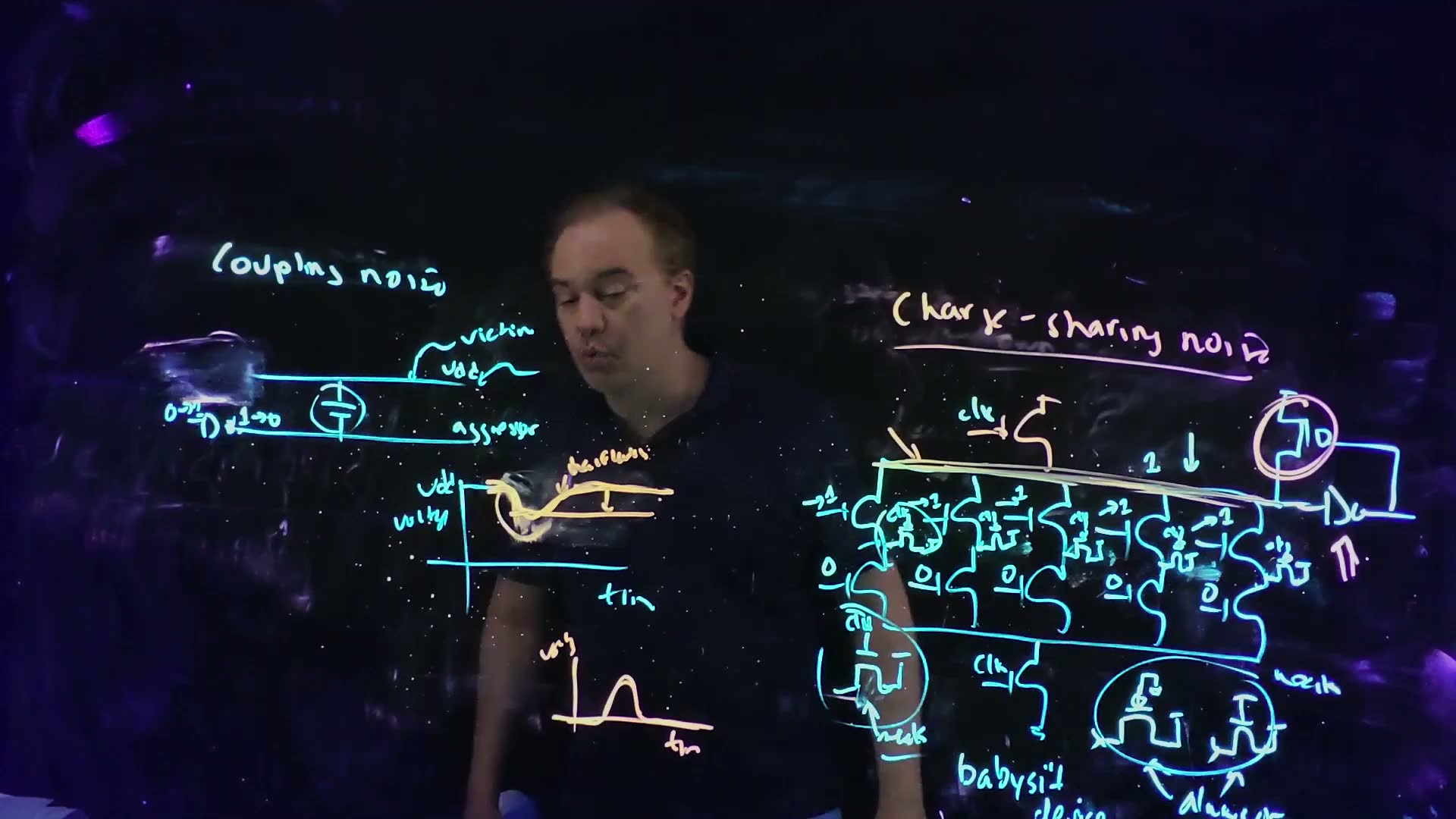
Two wires that run next to each other, or one above the other, have a capacitance between them (47:57) board. When one of them switches (the aggressor), the other (the victim), which should stay quiet, sees a blip (48:43–49:09). If the victim is driven, its driver pushes it back. How big the blip is depends on the coupling capacitance relative to the victim’s other capacitance and on the strength of the victim’s driver; the course quantifies it later, with interconnect (49:09–49:37).
Two places where it hurts a dynamic gate:
- On an input (49:48). A blip on one of the pull-down’s inputs can turn its NFET on briefly and discharge the dynamic node: a false evaluation that the input’s own recovery doesn’t undo (Section 4: a dynamic node can’t recover).
- On the dynamic node itself (50:20). A truly floating node, pulled down by a switching aggressor, “will never recover” board. With a half latch it does recover, unless it dropped far enough to switch the inverter first, in which case the gate glitches, and the glitch may be caught by a latch (50:51–51:27).
The defences (51:27–51:57): size the half latch for it, and in layout protect the dynamic node: no significant aggressors next to it.
Check yourself A dynamic gate's input is driven by a strong inverter that holds it at 0. A neighbouring wire switches, and the input blips up to 0.4 V for 20 ps before its driver pulls it back. Why can the gate still give the wrong answer?
During the blip the input’s NFET is partly on and drains charge from the dynamic node. When the input returns to 0, nothing puts that charge back until the next precharge (49:48). If the node has lost enough to cross the inverter’s switching threshold, the output is wrong for the rest of the cycle.
12. Power-supply noise
The idea. If the supply is low when the node is precharged and high when it is read, the inverter sees the difference as noise.

The supply is not constant (52:43) board. Many circuits switching at once draw current through the impedance of the supply network, and the rails droop, or collapse toward each other and back, ringing together (53:06–53:48). Power-distribution networks, decoupling capacitance and grids to reduce resistance and inductance come later, with interconnect (53:48–54:19).
The effect on a domino gate (54:52–56:11) board:
- Suppose the precharge happens when is at its lowest, . The dynamic node is charged to and then floats.
- In evaluate the supply has come back up to . The inverter now compares the stored against its own higher supply.
- To the inverter the node looks low by board: a DC noise on the dynamic node.
The fixes (56:11–56:41): first, reduce the supply noise itself. Second, the half latch: its source is tied to , so as the supply rises it pulls the node up with it, and the node tracks .
Next lecture (56:56). How to size dynamic logic with the same gain-based method as static CMOS, and the speed it gains from dropping the PFETs; two variants of domino, zipper logic and delayed-reset domino; then latches and clocking. The sizing and the two variants are in Chapter 12; latches are past the midterm.
Check yourself A domino gate is precharged while the supply has drooped to 1.1 V; in evaluate the supply is back at 1.2 V. Its inverter switches at 0.6 VDD. On top of that, the charge sharing of Section 10 (CX = 40 fF, Cint = 24 fF) occurs. Does it falsely evaluate? Would either problem alone?
Charge sharing from 1.1 V: , below the 0.72 V switching point: it falsely evaluates. Supply noise alone leaves 1.1 V (fine); charge sharing alone, from 1.2 V, leaves 0.75 V (just fine). Noise sources add, which is why each one must be kept well inside the margin. A half latch would help with both.
Formulas to remember
| Formula | Meaning |
|---|---|
| pseudo-NMOS: low not at ground; static current when low | the two problems of ratioed logic; turn the load off for tests |
| equal widths: NFET down, up; PFET up, down | the lecture’s pass-transistor model |
| down, up | so the pass PFET is sized equal to the pass NFET; size with the driver (one CCC) |
| exactly one / both / neither network connected | static / ratioed / dynamic |
| clk = 0 precharge (node to ); clk = 1 evaluate | the dynamic gate; a floating 1 is held only by charge |
| footer: clocked NFET at the foot, in series | prevents collisions in precharge; counts in the evaluate stack |
| node , domino output | is the pull-down’s switching function; domino is non-inverting |
| delay , footer included | evaluate delay; the precharge device is off |
| dynamic into dynamic on one clock: a race | cured by the domino inverter (precharged outputs are 0) |
| strong-PFET inverter after the node | skewed; switches higher, smaller for the node |
| half latch ≈ 1/10 of the pull-down’s strength | weaken by W↓, then a series device with long L; the output-driven device at , |
| , internal nodes ≤ | charge sharing (added); fixed by babysit devices and the half latch |
| precharged at , read at : noise | supply noise; the half latch makes the node track |
The lecture’s boards