18. PLAs and memory organization: NOR–NOR planes, replica clocks and the SRAM array
A processor has three kinds of circuit: the datapath (Chapters 16 and 17), the control logic that steers it, and the memory arrays. Lecture 17 takes the last two. Control logic is “random”: it has no regular structure and keeps changing until the chip is taped out. One way to build it is to synthesize it and place and route the gates. The other, this chapter’s, is to write it as a sum of products and lay it out as a regular two-level array, the programmable logic array (PLA). By De Morgan’s laws both levels can be NOR gates. The static PLA builds them in pseudo-NMOS; the dynamic PLA clocks them, and then needs two clocks whose edges are timed by copies of its own rows, a self-timed trick that SRAMs use too. The last part of the lecture opens the third kind of block: the SRAM array, its word lines and bit lines, and how the address bits are split between the rows and the columns. The PLA example begins at the end of Lecture 16 (54:46), and this chapter starts there.
After this chapter you can:
- turn a sum of products into a NOR–NOR network and name its AND and OR planes;
- draw a static PLA’s row as a pseudo-NMOS NOR and say what “ratioed” costs;
- program a PLA for given functions: one row per product, a device on the complement line for a true literal;
- read a PLA’s outputs off its transistors, with or without output inverters;
- write a function as an Espresso table and cut its product terms by hand;
- read a few lines of a VHDL state machine into table rows;
- explain the dynamic PLA’s race and the two timing requirements its clocks must meet;
- trace the replica rows that generate φAND and φOR, edge by edge, and time them with given delays;
- split a memory’s address bits between the row decoder and the column multiplexer for any physical organization.
Boxes and equations marked board were written in the lecture. Parts marked added are explanations or examples this guide adds.
Symbols
| Symbol | Meaning | Unit | First appears |
|---|---|---|---|
| ; | the inputs and their complements: the literals (the board’s names) | — | §1 |
| , | the example’s two outputs (board) | — | §1 |
| , | an OR-plane column’s own output, before the output inverter (the board’s equations) | — | §1 |
| product rows, top to bottom (the guide’s names; the board labels each row by its expression) added | — | §1 | |
| SOP | sum of products: an OR of AND terms | — | §1 |
| the supply | V | §2 | |
| a gate’s output node | — | §2 | |
| , , | the rows and output of §4’s practice PLA added | — | §4 |
| 1, 0, – | Espresso’s table codes: literal true, complemented, absent; in the output part, 1 = the output uses the product | — | §5 |
| cs, ns | current state and next state of a state machine (board) | — | §6 |
| hl1, hl0, fl1, fl0, st | the controller’s outputs: highway and farm-road lights (two bits each) and start-timer (board) | — | §6 |
| cars, short, long | the controller’s inputs: the car sensor and the timer’s two flags (board) | — | §6 |
| clk, | the input clock and its complement | — | §7 |
| , | the AND plane’s and the OR plane’s clocks (board); each plane precharges while its clock is low | — | §7 |
| , | outputs of a PLA without output inverters (as FN19 names them) | — | §7 |
| , | the replica rows’ outputs in the φAND and φOR generators added | — | §9 |
| , | an inverter’s and a NAND’s delay added | ps | §8 |
| , | a replica row’s precharge time and its evaluate time through one on device added | ps | §8 |
| PVT | process, voltage and temperature (board) | — | §8 |
| , | a memory’s number of words and bits per word (its logical organization) added | — | §10 |
| , | its physical rows (word lines) and columns (bit lines) added | — | §10 |
| WL, bit, | a word line, and the pair of bit lines of one column | — | §10 |
1. Control logic as a sum of products, built from NORs
You need
Gates and bubbles. A NOR’s output is 1 only when every input is 0. An inverter flips its input. A small circle (a bubble) on a gate’s input or output stands for an inverter there.
De Morgan’s laws added (background from earlier courses):
Read the first one backwards with and in place of and : . An AND of and is a NOR of their complements.
Sum of products added. A literal is an input or its complement ( or ). A product term is an AND of literals (). A sum of products is an OR of product terms, and every logic function can be written as one (one product per input row where it is 1, at worst).
The question. Control logic has no regular structure, and it keeps changing until the chip is taped out. How can any such function be built from one kind of gate, laid out as a regular array that is easy to change?
Two ways to build control logic
The lecture recalls Lecture 16’s split board (L16 43:29–46:44; L17 00:52–02:59). Of a processor’s three kinds of circuit (datapath, control, arrays: Chapter 15’s taxonomy), the control logic is the “random” one. It can be built in two ways:
- Multi-level logic, by the semi-custom flow: a synthesis tool turns the description into gates and a place-and-route tool lays them out. The result has no visible structure; the board brackets it as “random logic”. (Chapter 17 sketches the flow.)
- Structured control logic: write each output as a sum of products and build it as two levels of logic in a regular array, the PLA. Adding a product adds a row; changing a function moves transistors in the grid.
The example
The example that runs through the whole chapter board (L16 55:42; L17 06:40) has three inputs , , , each available true and complemented, and two outputs:
There are four different product terms, , , and , and one of them, , is shared: both outputs use it. The PLA will give each product one row, so this PLA has four rows, not five.
AND–OR to NOR–NOR in three moves, then the planes
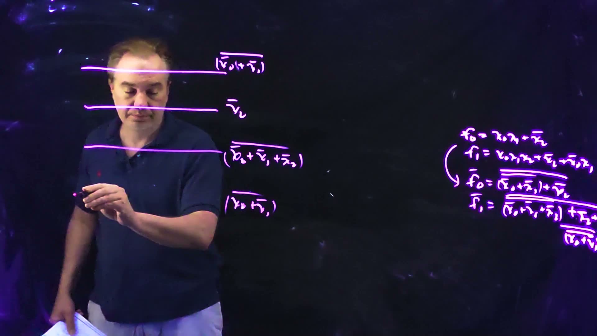
Lecture 16’s last board draws the conversion for in four stages board (L16 56:06–57:42; frames 57:25, 58:10).
From AND–OR to NOR–NOR, drawn for (the board, Lecture16 @ 58:10, draws the same stages for generic AND terms; the middle stage is read at 57:25). (a) The sum of products as an AND feeding an OR. (b) An OR is a NOR followed by an inverter. (c) Invert each AND input twice, by an inverter and a bubble, which changes nothing; an AND with bubbled inputs is a NOR (De Morgan), so the AND becomes a NOR of and . (d) The NOR–NOR form: complemented literals into the first column of NORs, the AND plane, whose outputs feed the second column, the OR plane, then an output inverter. The single literal becomes a one-input NOR of , which is an inverter.
The board (Lecture16 @ 58:10)

Fair copy of the board above (Lecture16 @ 58:10), mark for mark in its own layout. All black: one blue pen wrote the board (it looks violet towards the left edge, where the light shifts its hue). The box round the equations is still being drawn: its left side and top are there, and the pen is on its right end. The arrow after the second stage and the inverters of the third, washed out by the lecturer’s raised hand here, are copied from 57:25. The board draws each inverter as a small D shape with a bubble, and writes the of over a first attempt.
Three moves on the first output, then the planes (board, L16 56:06–57:42; L17 02:59)
- Write the sum of products as gates. is an AND of and , ORed with the literal : two levels, AND then OR (panel a).
- Make the OR a NOR and an inverter. : a NOR gives , and an inverter after it gives back (panel b). The output column now computes , and the inverter turns it into .
- Make each AND a NOR of complements. Put an inverter and a bubble on each AND input: two inversions change nothing. An AND with bubbled inputs is a NOR, by De Morgan, ; so the AND becomes a NOR fed with and (panel c). The literal needs no AND; written as a NOR it is a one-input NOR of , an inverter.
- Read off the two planes. Complemented literals go into a column of NORs; their outputs go into a second column of NORs; an inverter follows (panel d). The first column does the work of the ANDs, so it is called the AND plane; the second does the work of the OR, the OR plane. “They’re still both NORs” (02:36).
All four products as NORs
The same move on each of the example’s four products board (L17 08:15 writes all four at the ends of the rows), giving the rows their names added:
Look at : its literal is already a complement, so its NOR takes the complement of the complement, . Every literal enters its NOR flipped: a true literal as its complement, a complemented one as the true input. The outputs are then NORs of the rows, followed by inverters:
and each output is its column inverted, .
Memorize or derive. Derive both, in one line each from De Morgan; what to memorize is the result in words: a product is the NOR of its literals’ complements, and a column of the OR plane gives the complement of the output until an inverter follows it.
A worked example added. Check the NOR–NOR form of on two input rows, written .
f0 through its NORs, two input rows
- Row 110. ; ; ; . Directly: . They agree.
- Row 001. ; ; ; . Directly: . They agree.
Traps.
- Feeding a product’s NOR its true literals. : the product of the complements, the wrong function. Each literal goes in flipped.
- Forgetting the output inverter. The OR plane’s NOR gives , not . Whether an inverter follows decides every output bit (Section 4).
- Counting a shared product twice. appears in both outputs but is one product: one AND-plane NOR, used by both OR-plane NORs.
Check yourself Write the product x̄0x1 as a NOR.
: each literal enters flipped, so enters as and as .
Check yourself Write f1's OR-plane column as a NOR of NORs, and say which product it shares with f0.
, and is its inversion. It shares with , whose column is .
2. The static PLA’s gate: a pseudo-NMOS NOR
You need
Pseudo-NMOS (Chapter 10 §10). A PFET whose gate is tied to ground is always on; it pulls the output up, against a pull-down network of NFETs. With every NFET off the output is . With any NFET on, that NFET overpowers the weak PFET and pulls the output low, but not to ground: the low settles where the two currents balance, so it depends on the ratio of their strengths (ratioed logic). And while the output is low, current flows from to ground all the time (static power).
A complementary CMOS NOR (Chapter 7). A -input NOR has parallel NFETs and PFETs in series: devices, and a pull-up stack high whose PFETs must each be about times wider to keep the rise time, so a wide NOR is large and slow.
The question. A PLA’s NORs must be as wide as the function needs: a row may have a device for every input, a column one for every product. What gate makes a NOR of any width cheap?
Arbitrarily wide NORs
The static PLA uses pseudo-NMOS board (03:46, 04:37). One PFET with its gate grounded is the load; one NFET per input hangs in parallel from the output to ground. Adding an input adds one NFET and nothing in series.
The pseudo-NMOS NOR, redrawn from the board (Lecture17 @ 04:37). The PFET’s gate is grounded, so it is always on: a weak load. Any input at 1 turns its NFET on and pulls low; with all inputs at 0, is high. So . The dots: another input is one more NFET in parallel, with nothing added in series.
The board (Lecture17 @ 03:46)

Fair copy of the board above (Lecture17 @ 03:46), mark for mark in its own layout. All black: a violet pen wrote the recap list, from “Multilevel” to “PLA”, and “random logic”; a pink pen wrote everything from “SOP (sum of products)” on. The pink writes the next topic rather than marking over the first, so it takes no accent. The NFETs have no gates yet, and the PFET is not yet ringed: both come by 04:37. The second and third NFETs, behind the lecturer’s hand here, are copied from 04:37. “AND pla” is the board’s shortened “AND plane”.
“The whole idea of doing these as NORs is that they can be arbitrarily wide … it uses pseudo-NMOS. Okay, so it’s ratioed logic” (03:01–03:25). All of the logic sits in the pull-downs. A static PLA is a pseudo-NMOS NOR plane feeding a pseudo-NMOS NOR plane, laid out as a grid (03:50–04:21); Section 3 builds one.
What pseudo-NMOS costs
The costs are Chapter 10’s added:
- The low is not ground. A low row or column sits at the level where the on NFETs and the always-on PFET balance. The NFETs must be clearly stronger than the PFET, or the next gate does not see a low.
- Static current. A row or column that is low draws current from through its PFET the whole time it is low.
- A slow rise. The rising edge comes through the one weak PFET.
The lecture’s cure is the dynamic PLA (Section 7), which replaces each PFET load with a clocked precharge device. The name stays: “it’s an unfortunate name because it’s not static logic, it’s actually ratioed logic, but it’s still called a static PLA” (36:06–36:24).
A worked example: counting devices
added Count the devices of the example’s static PLA (its NOR forms are in Section 1, repeated here): rows , , , ; columns and .
The example's static PLA, device by device
- AND plane. One NFET per literal in each row: NFETs, and one PFET load per row, 4.
- OR plane. One NFET per row a column uses: NFETs, and one PFET per column, 2.
- Total. devices before the inverters; with the two output inverters, of two devices each, 23. (The three input inverters that make , , add 6 more; they are not counted here.)
- Against complementary CMOS. The widest row, , is a 3-input NOR: in pseudo-NMOS 4 devices, all but the load in parallel; in complementary CMOS 6, with 3 PFETs in series.
Traps.
- Calling the static PLA static logic. It is ratioed: non-rail lows and static current (36:06).
- A strong pull-up. A PFET load as strong as the NFETs lifts the low toward the middle of the swing (Chapter 10), and the next plane may read it as a 1.
Check yourself How many devices does a 6-input pseudo-NMOS NOR need, and a 6-input complementary CMOS NOR?
Pseudo-NMOS: 6 NFETs and 1 PFET, 7. Complementary: 6 NFETs and 6 series PFETs, 12.
Check yourself When does a static PLA row draw static current? On how many of the 8 input rows does the example's row P0 (= x0x1) draw it?
A row draws current whenever it is low, that is, whenever one of its devices is on, which is whenever its product is false. is true on 2 of the 8 input rows (110 and 111), so it draws static current on the other 6.
3. Programming a PLA: the worked example
You need
The example in NOR form (Section 1). Rows , , , ; columns , , each followed by an inverter. A product is the NOR of its literals flipped.
One row is a pseudo-NMOS NOR (Section 2): a grounded-gate PFET load and one NFET per input, in parallel to ground. An NFET whose gate is 1 is on and pulls the row low.
The question. Section 1 gave the network as gates. How is it laid out as a grid, and what does “programming” the grid mean?
The grid: literal lines, ground lines and rows
The lecture builds the grid step by step board (08:15–14:52).
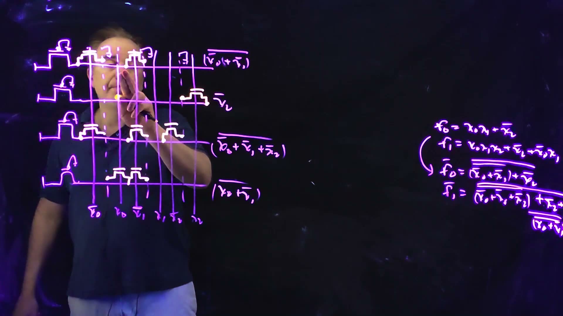
The example’s static PLA, redrawn from the board (Lecture17 @ 14:52; the rows behind the lecturer from 12:08). Dashed lines are ground lines. AND plane (left): each row starts at a pseudo-NMOS pull-up; an NFET sits where a row crosses a literal line it needs, gate on the line, one terminal on the row and the other on the ground line beside it. OR plane (right): each column has a pull-up at the top and an NFET at each row it uses, gate on the row. The board’s columns end at , ; the output inverters to , are added.
The board (Lecture17 @ 14:52)
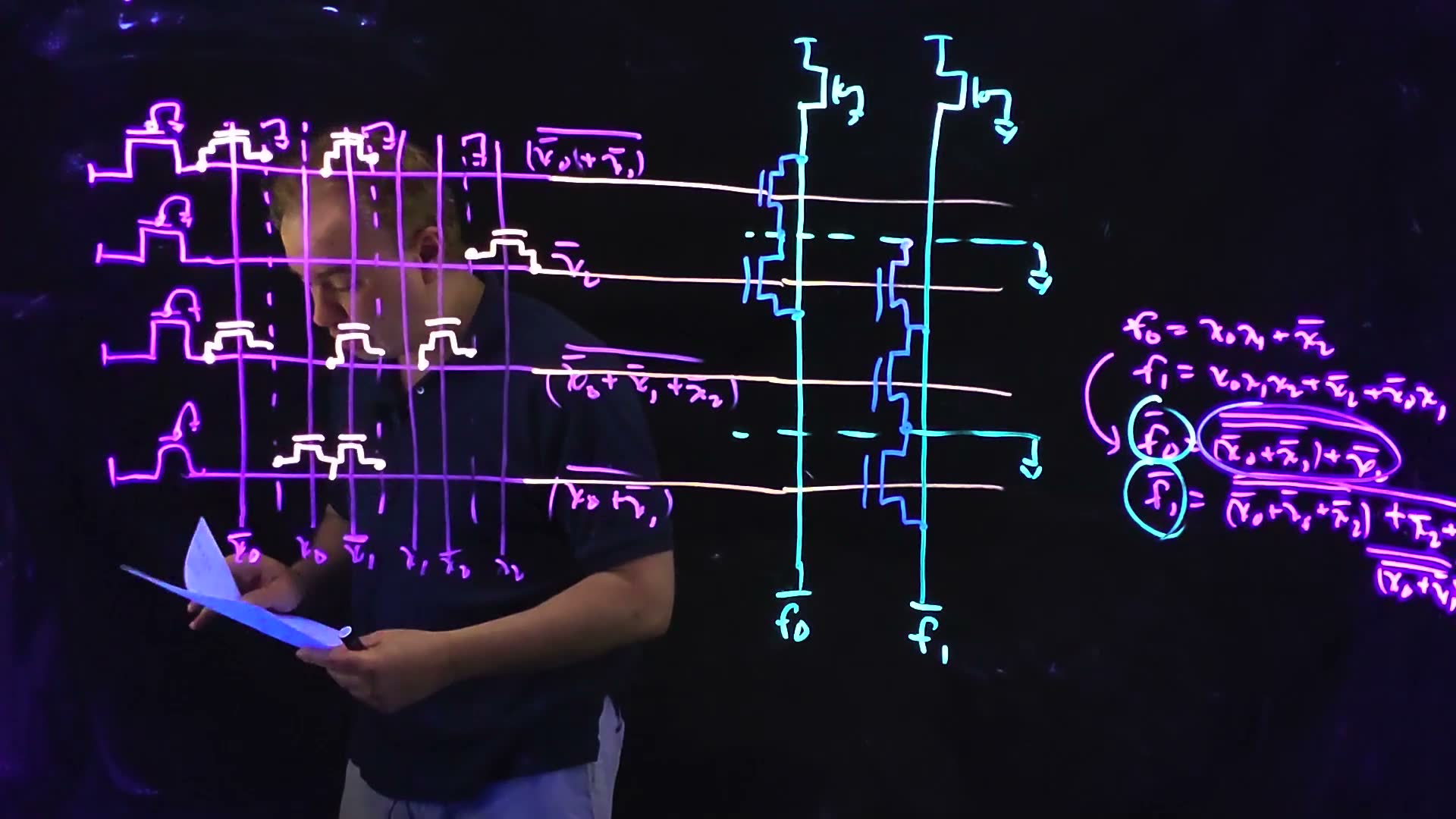
Fair copy of the board above (Lecture17 @ 14:52), mark for mark in its own layout. Black is the violet pen: the AND plane’s pull-ups, rows, literal lines and dashed ground lines, the row expressions, the bottom labels and the equations, with the ring round the right side of ‘s equation. Orange is the pale cream pen: the AND plane’s eight devices with their dots, and the rows’ extensions into the OR plane. Teal is the cyan pen: the OR plane, its labels and the rings on and . The bars above and at the bottom are the columns’ end bars, so each column gives (Section 3). The bottom labels, partly behind the papers in the lecturer’s hands here, are read on 14:07. The equation for runs off the frame’s right edge and is copied to the edge.
Laying out the example (board, 08:15–14:52)
- One row per product (08:15). Four horizontal lines, , each with a pseudo-NMOS pull-up at its left end: a PFET from with its gate grounded. The board writes each row’s NOR at its right end.
- The literal lines (08:58–10:17). Vertical lines carry every literal, true and complement: , , , , , (the complements come from inverters at the bottom). Between each pair runs a ground line (dashed). Every row crosses every literal line, but a crossing does nothing until a transistor is put there.
- Programming a crossing (10:23). To make a literal line an input of a row’s NOR, drop an NFET at the crossing: its gate on the literal line, one terminal on the row, the other on the neighbouring ground line. When the line is 1, the device is on and pulls the row low (the enlarged crossing, right after these steps).
- Program each row from its NOR (10:23–12:08). : devices on the and lines. : one device, on (a one-input NOR is an inverter, which makes ; 10:57). : devices on , , . : devices on and . The rule: a literal that appears true in the product gets its device on the complement line, and a complemented literal on the true line.
- The OR plane (12:19–14:24). The rows run on to the right and cross two vertical output columns, each with its own pull-up at the top, and horizontal ground lines between the rows. Column gets devices at and ; column at , and . Each device’s gate is on the row. Row feeds both columns: the shared product is built once.
- The outputs added. Each column computes a NOR of its rows, the complement of its output: the board names them and (12:51). An inverter after each column gives and ; the board stops at the columns.
One programmed crossing, enlarged added (row ‘s device on the line, from the board at 14:52). The NFET’s gate sits on the literal line; its terminals connect to the row and to the ground line beside it. When its literal is 1 the device is on and pulls the row low (the arrow). Beside it, at the line, there is no device: the row and the line cross without connecting.
“The way I’ve drawn the schematic is basically going to be reflective of how this is going to be laid out” (11:54–12:19). The schematic is the floor plan: programming the PLA is choosing where transistors go in a fixed grid.
The two formulas, and the whole truth table
Memorize or derive. Derive: both are Section 1’s NOR read off the grid. A row’s devices sit on the complements of its literals, so the NOR of those lines is the AND of the literals.
A worked example: the board’s PLA, evaluated. Every row and both outputs for all eight inputs added, rows written :
| 000 | 0 | 1 | 0 | 0 | 0 | 0 | 1 | 1 |
| 001 | 0 | 0 | 0 | 0 | 1 | 1 | 0 | 0 |
| 010 | 0 | 1 | 0 | 1 | 0 | 0 | 1 | 1 |
| 011 | 0 | 0 | 0 | 1 | 1 | 0 | 0 | 1 |
| 100 | 0 | 1 | 0 | 0 | 0 | 0 | 1 | 1 |
| 101 | 0 | 0 | 0 | 0 | 1 | 1 | 0 | 0 |
| 110 | 1 | 1 | 0 | 0 | 0 | 0 | 1 | 1 |
| 111 | 1 | 0 | 1 | 0 | 0 | 0 | 1 | 1 |
One input row through the grid: x0x1x2 = 011
- The literal lines. , ; , ; , .
- Row has devices on and . turns one on, so the row is pulled low: .
- Row has its device on : on, . Row : its device is on, .
- Row has devices on and : both off, so the pull-up holds the row high, .
- The columns. uses and , both 0, so no device is on: and . uses , , ; turns its device on: and .
- Check against the functions. and . They agree.
Traps.
- The device on the true line for a true literal. A row with devices on and computes : the product of the complements.
Check yourself Row P3 computes x̄0x1. On which literal lines are its devices?
On and : each literal’s device sits on its complement’s line, so the row is .
Check yourself Add a third output f2 = x̄2 + x̄0x1. Does the AND plane change? How many devices are added, and where?
No new row: both products already exist ( and ). Add a third OR-plane column with NFETs at rows and , a pull-up PFET at its top and an output inverter: 5 devices.
4. Reading a PLA back to its functions
You need
A programmed crossing (Section 3). An NFET with its gate on a literal line and its terminals on the row and on a ground line. It is on when its literal is 1, and an on device pulls its row (or column) low. A crossing without a device does nothing.
Rows and columns are NORs (Section 3). A row is the NOR of the lines its devices sit on; a column is the NOR of the rows it has devices at:
A NOR of complemented literals is the AND of the literals (De Morgan), so a row with devices on and is .
The question. The lecture only builds PLAs from their functions. Both PLA questions on the past finals run the other way: here are the transistors, what are the outputs? What is the routine for reading a PLA, and where does it go wrong?
The routine
added Three steps, and two decisions that carry the marks: which line each device’s gate sits on, and whether the paper draws output inverters.
Reading a PLA
- Rows. For each row, list the lines its devices’ gates sit on. Flip each line’s literal, and AND them: devices on and give ; one device on gives . (The row is the NOR of those lines, and De Morgan turns a NOR of lines into the AND of their complements.)
- Columns. Each column is the NOR of the rows it uses. If an inverter follows, the output is the OR of those rows. If not, it is the complement of that OR: simplify it with De Morgan.
- Simplify and check. Simplify each output, then check two input rows by tracing them through the grid (Section 3’s walk), not through your formula.
A dynamic PLA (Section 7) is read the same way: once both planes have evaluated, each row and each column holds the NOR of its inputs.
The board’s PLA, read backwards
Take Section 3’s PLA as if it were an exam’s figure, with nothing said about its functions.
Reading the example's PLA (added)
- Row : devices on , . Flip and AND: .
- Row : one device, on : .
- Row : devices on , , : .
- Row : devices on , : .
- Columns, with the inverters. Column 1 uses and : . Column 2 uses , , : .
- Simplify added. Split on . If , and . If , . So : it is 1 when or . (This takes three products in place of four; Section 5 uses it.)
- The same grid without inverters. Each output is the column’s own NOR: and .
- Check two input rows by tracing. 011: from Section 3’s walk, and , so , ; the formulas give and . 101: every row is pulled low ( by , by , by , by ), so both columns are high and ; the formulas give and . Without inverters, 101 gives , and , .
The truth tables added, rows :
| 000 | 001 | 010 | 011 | 100 | 101 | 110 | 111 | |
|---|---|---|---|---|---|---|---|---|
| 1 | 0 | 1 | 0 | 1 | 0 | 1 | 1 | |
| 1 | 0 | 1 | 1 | 1 | 0 | 1 | 1 | |
| (no inverter) | 0 | 1 | 0 | 1 | 0 | 1 | 0 | 0 |
| (no inverter) | 0 | 1 | 0 | 0 | 0 | 1 | 0 | 0 |
Traps.
- Reading a device by its terminals. The literal is the line its gate sits on. Its terminals touch the row and a ground line, never another literal line.
- Reading through a missing inverter. If the paper’s columns run straight to the outputs, the outputs are complements of the sums. Look for the inverter before writing anything.
- Stopping at an unsimplified form when the question asks for “the function”. An unsimplified sum is correct, but simplify it, and check that the two forms agree on every input row.
A PLA to read added, in the style of the example’s. Dashed lines are ground lines. The rows carry no expressions: find them from the devices. The column ends at with no output inverter.
Check yourself The PLA in the figure has rows Q0 (devices on x0 and x1) and Q1 (devices on x̄0 and x2), and one column z using both, with no inverter. What is z, and what is its truth table for x0x1x2 = 000 … 111?
and . With no inverter, . For this is ; for it is . So , with truth table 0, 0, 1, 1, 0, 1, 0, 1.
Check yourself Put an inverter after the same column. What is the output now, and on how many of the eight input rows is it 1?
The inverter undoes the column’s NOR, so the output is the OR of the rows: . It is the complement of ‘s table, 1, 1, 0, 0, 1, 0, 1, 0: 4 rows (000, 001, 100, 110).
Remember. The two past-final PLAs are this chapter’s example. FN12-10a draws its first three rows, static, with output inverters (there simplifies to itself, a ready case of the simplify trap); FN19-6a draws all four rows, dynamic, without them. The datapath practice page (FD1) solves both.
5. Fewer product terms: Espresso and its table
You need
A PLA’s rows are its products (Section 3). Each distinct product term is one AND-plane row, used by every output column that needs it. So the PLA’s height is its number of distinct products.
Implicants added. A product is an implicant of a function if it is 1 only on input rows where the function is 1. A sum of products is the function exactly when its products are implicants and together cover every 1.
The device rule (Section 3): a literal that appears true in a product has its device on the complement line; a complemented literal, on the true line.
The question. Fewer products means fewer rows, a smaller and faster PLA. How do we find a small set of products, shared between the outputs, and how does a tool take the functions in?
Minimizing is hard; Espresso does it well
“The optimization to try to minimize the number of product terms is an NP-complete problem, as most interesting problems are in CAD” (15:24–15:59). The tool used in the course’s problem sets is Espresso board, a heuristic two-level minimizer: its result is “not provably minimum, but in practice minimum” (16:30–17:03). It also maximizes sharing: one product used by several outputs costs one row.
The table format
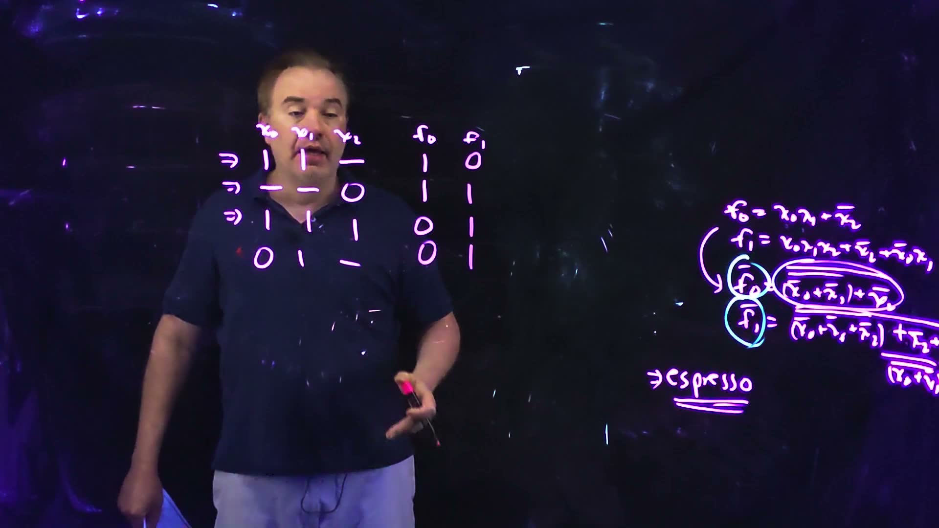
Espresso reads a table board (17:09–20:25): one line per product, with an AND part and an OR part.
- AND part, one column per input: 1 if the literal appears true, 0 if it appears complemented, – if the input is absent from the product.
- OR part, one column per output: 1 if the output uses the product.
The example’s table, as the board writes it:
| product | |||||
|---|---|---|---|---|---|
| 1 | 1 | – | 1 | 0 | |
| – | – | 0 | 1 | 1 | |
| 1 | 1 | 1 | 0 | 1 | |
| 0 | 1 | – | 0 | 1 |
The board’s speech says the OR part has “a one if I use that literal” (19:01): a slip for product term; the 1s choose products.
The Espresso table and what it programs. Top left: the example’s table, from the board (Lecture17 @ 20:25). Top right added: the example minimized by hand to three products (this section’s worked example). Bottom added: the first line, 1 1 –, as the PLA row : each 1 puts a device on the literal’s complement line, and the – leaves ‘s pair empty, so the row computes .
The board (Lecture17 @ 21:05)

Fair copy of the board above (Lecture17 @ 21:05), mark for mark in its own layout. Black is the violet pen: the table and its arrows, the equations, and “espresso”, boxed and double-underlined, with the arrow into it. Teal is the cyan pen’s rings on and , left from 14:52: the planes are wiped, and the equations are unchanged and copied as at 14:52. The short strokes under the header, the lone 1 right of the first row, the stroke right of the last row and the corner marks under it are copied as they stand. The lecturer stands in front of the table’s middle; every digit shows through, and 20:25, where he stands clear, has the same ink.
From a table line to a PLA row, and back (added)
- AND part to devices. A 1 in column means the product contains , so its device goes on the line; a 0 means it contains , device on the line; a – means no device on either. Line 1, 1 1 –: devices on and , which is row of Section 3.
- OR part to columns. Line 2, – – 0 | 1 1: the product (device on the line), used by both outputs, so both columns get a device at that row.
- Backwards. A row with devices on and is : code 0 1 –.
Espresso returns a table with fewer lines that keeps every output the same (19:40–20:11). The lecturer adds a remark about colleagues earlier in his career (at IBM, 35:31) who wanted all logic written in table formats (20:17–20:57). The idea did not catch on, but RTL code reduces to these tables, as Section 6 shows.
A worked example: three products instead of four
added Minimize the example by hand. (The lecture says Espresso would hand this table back unchanged; for this function it can be cut, as follows.)
Cutting the example to three rows
- alone. : two products, and neither can be dropped. alone misses rows 000, 010, 100, where ; alone misses 111.
- alone. Section 4 found : two products. The single literal , code – 1 –, is an implicant of (every row with has ) and covers both and .
- Share. serves both outputs. The cover is three rows: uses the first two, the last two. The table: 1 1 – | 1 0, – – 0 | 1 1, – 1 – | 0 1.
- Can two rows do it? An exhaustive search over all 27 products of three inputs (in the test) finds no two-product cover and eight different three-product covers. Three is the minimum. One of the eight, , is the board’s own table without its first line ( takes in place of ), so the board’s four rows were never the minimum.
- Check on all eight inputs. The new table gives = 1, 0, 1, 0, 1, 0, 1, 1 and = 1, 0, 1, 1, 1, 0, 1, 1, the same as the four-row PLA (Section 4’s table).
Rows of the PLA = distinct products in the cover. Memorize this: a product shared by two outputs is one row.
Traps.
- Writing the code as the device’s line. Code 1 means the literal is true, and its device sits on the complement line.
- Minimizing each output alone and stacking the results. and each need two products, four in all; shared, counts once, three in all.
- Calling Espresso’s answer the proven minimum. It is a heuristic; for small functions an exhaustive search (or a Karnaugh map) proves the minimum.
Check yourself Write the table line for the product x̄0x2, used by f1 only.
0 – 1 | 0 1: complemented (0), absent (–), true (1); only uses it.
Check yourself A table has the lines 1 – 0 | 1 0 and 1 – 1 | 1 0. Merge them, and say how many PLA rows you save.
The two products are and , used by the same output; their sum is , the line 1 – – | 1 0. One row instead of two: one row saved.
6. Background for the final: from VHDL to a table
You need
A state machine (Chapter 13 §1 and §9). A flip-flop holds the current state cs. Combinational logic computes the next state ns and the outputs from cs and the inputs. At each rising clock edge the flip-flop loads ns into cs.
Espresso’s table (Section 5): one line per product, 1/0/– in the input part, 1 for each output that uses the product.
The question. No past final asks about VHDL; this section is background. How does the description of a controller in a hardware language turn into a table that Espresso, and then a PLA, can take?
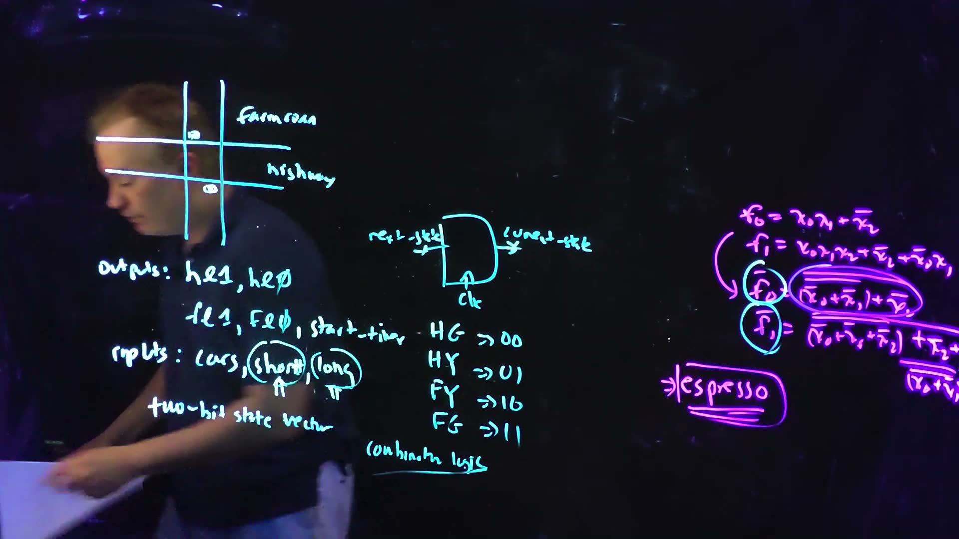
The lecture’s controller is the traffic light of Mead and Conway’s textbook board (22:17–27:19): a highway crossing a farm road, with a sensor on the farm road. Its outputs are two bits for each light, hl1, hl0 (highway) and fl1, fl0 (farm road), and st, which starts a timer. Its inputs are cars (the sensor) and short and long, which the timer raises after a short and a longer wait. A two-bit state register holds the state: HG = 00, HY = 01, FY = 10, FG = 11 (highway green, highway yellow, farm road yellow, farm road green).
The traffic-light controller, redrawn from the board (Lecture17 @ 35:01). Left: the highway (horizontal) and the farm road (vertical), with the car sensors on the farm road (the board draws two dots), and the state codes under it. Right: the combinational logic, which a PLA can implement, computes the lights, st and the next state ns from cars, short, long and the current state cs; the flip-flop loads ns into cs at each clock edge. The state codes are the board’s: highway green, highway yellow, farm road yellow and farm road green.
The board (Lecture17 @ 35:01)
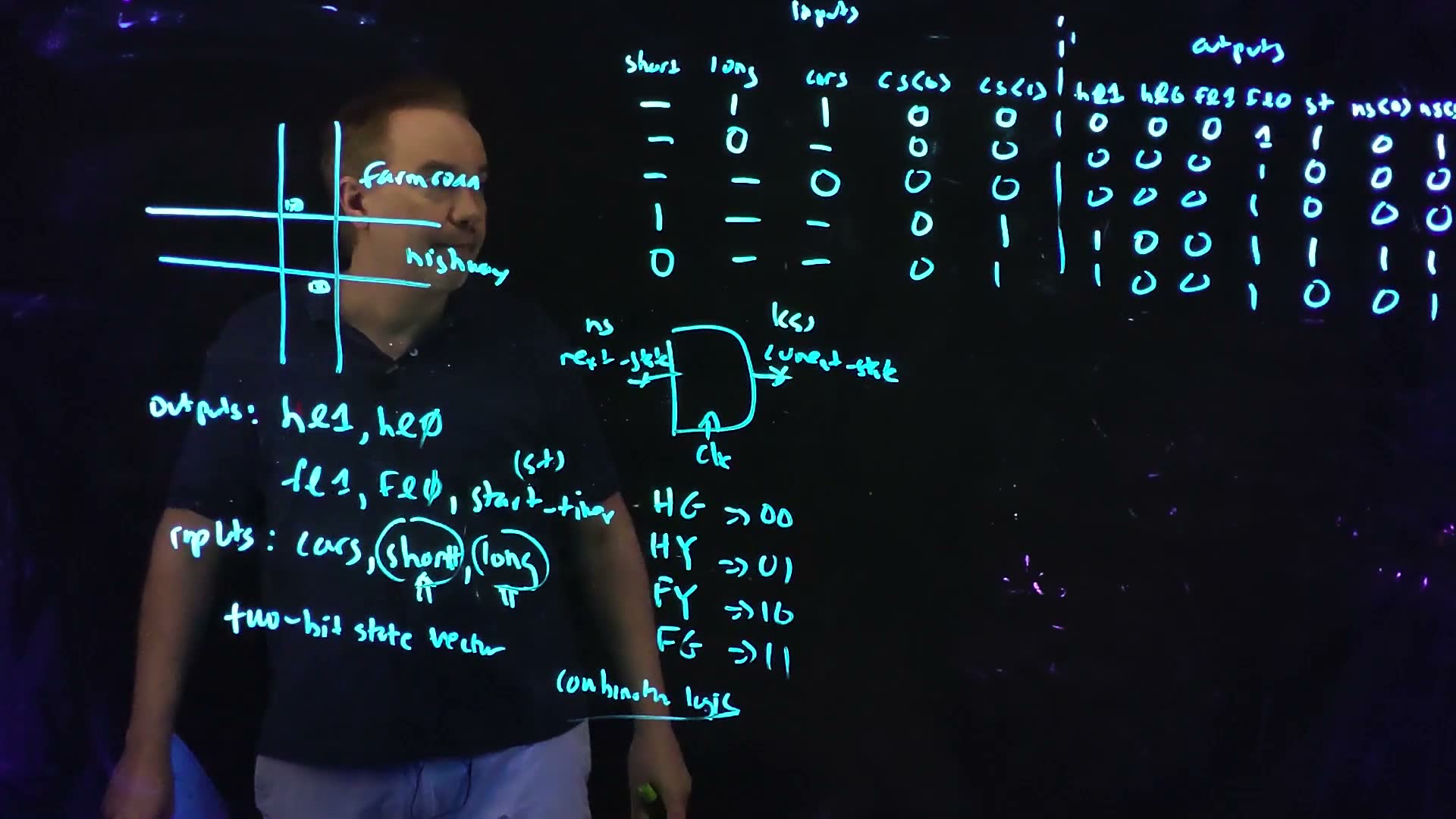
Fair copy of the board above (Lecture17 @ 35:01), mark for mark in its own layout. One pen (cyan) wrote the whole board, copied in black. The last header, ns(1), runs off the frame’s right edge and is cut there as the frame shows it. The table’s rows and the text lines are set level (the board’s rows drift down to the right). The board writes the zeros of hl∅ and Fl∅ slashed, and the F of Fl∅ and of the Fl1, Fl0 headers as a capital; both are copied as written.
The VHDL (spoken, 27:27–29:03; the handout itself is not among this guide’s sources). An entity lists the ports. A clocked process, with the test if clk = '1' and not clk'stable (a rising edge), is the state flip-flop. A combinational process first gives every output a default (ns = cs, the lights and st at 0), then a case on the current state with if branches on the inputs.
Into a table board (29:03–35:01). Each if branch becomes a product term: its conditions on the inputs and the state are the AND part, and the outputs it sets (with the defaults for the rest) are the OR part. The board writes the rows for HG and HY, twelve columns in the order short, long, cars, cs(0), cs(1) | hl1, hl0, fl1, fl0, st, ns(0), ns(1). Here they are grouped by signal, each group’s bits in the board’s order:
| short long cars | cs(0) cs(1) | hl1 hl0 | fl1 fl0 | st | ns(0) ns(1) |
|---|---|---|---|---|---|
| – 1 1 | 0 0 | 0 0 | 0 1 | 1 | 0 1 |
| – 0 – | 0 0 | 0 0 | 0 1 | 0 | 0 0 |
| – – 0 | 0 0 | 0 0 | 0 1 | 0 | 0 0 |
| 1 – – | 0 1 | 1 0 | 0 1 | 1 | 1 1 |
| 0 – – | 0 1 | 1 0 | 0 1 | 0 | 0 1 |
Read the first three in words. In HG (cs = 00), “if cars and long”: a car waits and the highway has had its minimum green, so start the timer and go to HY (ns = 01). Otherwise stay in HG. That else is “not cars or not long”, a sum of two products, so it takes two lines: long = 0, and cars = 0. The light bits in HG are hl = 00 and fl = 01; in HY the highway’s turns to hl = 10 (codes inferred from these two states). The rest is “an exercise” (35:02): RTL → table → Espresso → PLA, the path CAD tools once followed automatically (35:02–35:31).
Trap. Forgetting the defaults. A branch that does not assign st leaves it at its default, 0 (32:52–33:28), so its line has st = 0, not “don’t care”.
Check yourself Why does the else after “if cars and long” take two table lines, and what are their AND parts?
Its condition is the complement of cars·long, which by De Morgan is , a sum of two products. One line per product: long = 0 (– 0 – 0 0) and cars = 0 (– – 0 0 0). They overlap where both are 0, which is harmless: both lines set the same outputs.
7. The dynamic PLA and its race
You need
Precharge and evaluate (Chapter 11 §4). A dynamic gate has a clocked PFET from to its output node (the precharge device), its NFET network below, and a clocked NFET foot to ground. Clock low: the PFET is on and the foot off, so the node charges high. Clock high: the PFET is off and the foot on, so the node falls if the network conducts, and otherwise floats high. A node that has fallen cannot rise again until the next precharge.
The race (Chapter 11 §5). A dynamic gate’s output is high during precharge. A second dynamic gate driven by it therefore sees a 1 at the start of evaluate, whatever the first gate’s answer will be, and may discharge for good before the first gate falls. Domino cures it with an inverter after each dynamic gate, so that every input starts at 0.
The static PLA (Sections 2–3): rows and columns are pseudo-NMOS NORs, each with a grounded-gate PFET load.
The question. The static PLA’s loads burn static current and give lows above ground. Can each plane be made dynamic, and what goes wrong when one dynamic NOR plane drives another?
Clocking the planes
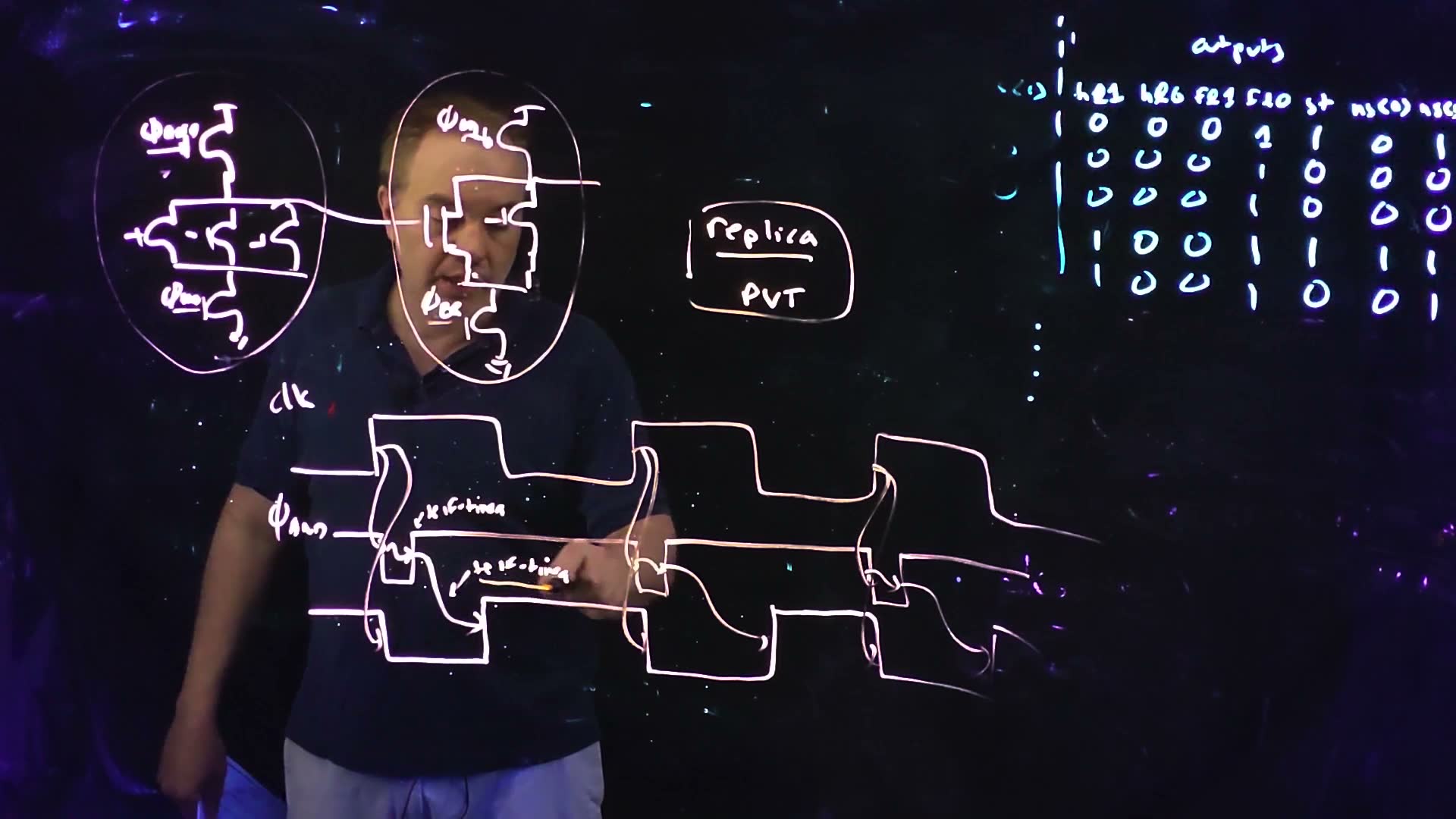
board (37:02–37:47). Take each pseudo-NMOS load and connect its gate to a clock: “make this the clock” (37:37). It becomes a precharge PFET. Add a clocked NFET foot under each row’s devices and under each column’s. Now each plane precharges while its clock is low and evaluates while it is high, draws no static current and pulls its lows all the way to ground.
One row of a dynamic PLA feeding one column, redrawn from the board (Lecture17 @ 43:07; first drawn at 37:47 with one clock, the frame folded in Section 8’s figure). Each plane’s precharge PFET and its foot share that plane’s clock: for the AND row, for the OR column. Clock low: precharge; clock high: evaluate. The row’s output drives an NFET gate in the column.
One clock on both planes: the race
The first drawing clocks both planes with the same clk (37:47). Then: “I’m gonna have the classic race condition … that caused us to actually go to domino logic and put an inverter here” (38:03). At the start of evaluate every row is still at its precharged high. Every OR-plane device is therefore on, so every column that has any device starts to discharge, whatever the inputs. A row whose product is false falls only after its own evaluate delay, and by then its column may have lost its charge for good. A NOR plane after a NOR plane has no inverter between them to cure this, and an inverter would break the NOR–NOR form.
The race with one clock on both planes added (a sketch of the lecture’s words at 37:51–38:29). When clk rises, a row whose product is false starts to fall, but it is still high for its whole evaluate delay (, the bracket). The column that it drives is evaluating at the same time, sees the row high, and discharges: a wrong 0 (✗) where the right value (dashed, ✓) is 1. The column cannot recover until the next precharge.
A worked example added. Take the example’s PLA, dynamic, with no output inverters (the form FN19-6 prints), so the outputs are the columns: and (Section 4).
What one shared clock does to the example
- At the start of evaluate, rows are all high, so both columns’ devices are on and both columns start to fall.
- In the worst case (a column that discharges faster than its false rows fall), then, at the end of evaluate, for every input.
- Count the errors. The correct is 1 on 3 of the 8 input rows (001, 011, 101) and on 2 (001, 101). Those are exactly the wrong outputs; every correct 0 is right by luck.
- The error is one-way. A precharged column can only fall during evaluate, so the race can only turn a correct 1 of the column into a 0 (with an output inverter: a correct 0 of the output into a 1).
The cure: two clocks, and the two requirements
The cure the lecture gives keeps the NOR–NOR form and clocks the two planes separately, by φAND and φOR board (38:29–38:43; labelled on the board’s circuit at 41:41). They must meet two requirements (40:06–41:53):
- Enough precharge time. φAND’s low pulse must last long enough to precharge the slowest AND row, and φOR’s low time long enough to precharge the OR plane.
- The OR plane waits. φOR must not rise (start the OR plane’s evaluate) until the slowest AND row has finished evaluating after φAND rose.
Memorize or derive. Memorize the two requirements in words; Section 8 shows why neither can be a fixed time, and Section 9 builds clocks that meet both.
Traps.
- “A slower OR plane cures it.” Any overlap of the OR plane’s evaluate with a row that is still high can discharge a column for good; only waiting cures it.
- The polarity. Precharge is clock low (the PFET on, the foot off); evaluate is clock high.
- Domino’s cure. An inverter between the planes would cure the race, but the planes are then no longer NOR into NOR.
Check yourself Which output values can the race corrupt in a PLA without output inverters: 0s or 1s? Why only those?
Only 1s. A column is precharged high and can only fall during evaluate, so the race can only discharge a column that should have stayed high. A column that should be 0 falls anyway.
Check yourself The slowest AND row takes 200 ps to fall through one device, but φOR rises only 150 ps after φAND. Which columns can go wrong, for how long is the danger open, and which way?
A column that should stay high (all of its rows false) but uses a row that is still falling: for up to ps that row is still high while the OR plane evaluates, its device is on, and the column can discharge to a wrong 0. Without an output inverter the output is a wrong 0; with one, a wrong 1. Requirement 2 is broken by 50 ps.
8. Two clocks with self-timed edges
You need
The two requirements (Section 7). Each plane precharges while its clock is low and evaluates while it is high. (1) φAND’s low pulse must be at least the slowest AND row’s precharge time , and φOR’s low time must cover the OR plane’s precharge. (2) φOR may rise only after the slowest AND row has evaluated, after φAND rose.
Synchronous design (Chapter 13 §1): only clock edges trigger events, and every delay is checked against the clock period.
The clock chopper (Chapter 14 §5): a NOR (or NAND) of a clock and a delayed, inverted copy of it makes one pulse a cycle, as wide as the delay: after each falling edge for the NOR, a low pulse at each rising edge for the NAND. Only one edge of the pulse is the clock’s; the other waits for the delay.
The question. How long is “long enough to precharge” and “after the slowest row has evaluated”? Both depend on the circuit’s own delays, which change from chip to chip and with the supply and the temperature. How can a clock edge follow them?
φAND: falls with the clock, rises when the rows are precharged
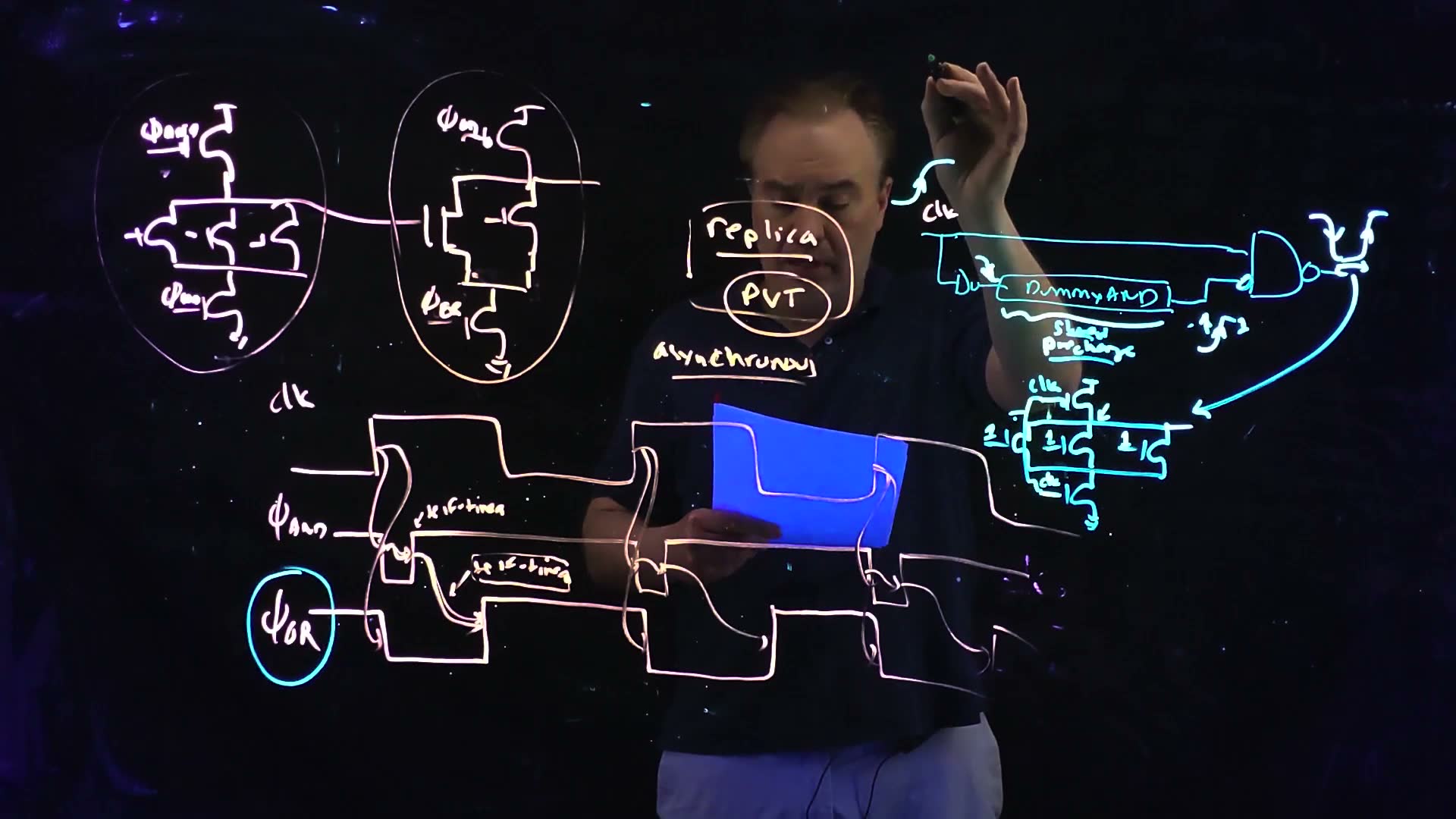
board (38:56–40:27). φAND falls at clk’s rising edge (the board’s curved arrow), which starts the AND plane’s precharge. Its rising edge is self-timed: it comes “just enough” later for the rows to precharge, and then the AND plane evaluates for the rest of the cycle. The delay is made by a replica: “a replica is a copy, just what it says, a replica of the circuit that I’m trying to estimate the delay for, that PVT tracks that circuit” (39:39). Laid out like the real rows, it slows down and speeds up with them at every corner of PVT: process, voltage and temperature.
φOR: rises when the rows have evaluated
board (40:44–41:53). φOR’s rising edge is timed from φAND’s rising edge, again self-timed, by a replica of the slowest row’s evaluate. So the OR plane starts to evaluate only after every AND row has settled: requirement 2.
The two clocks of the dynamic PLA, redrawn from the board (Lecture17 @ 43:07, uncovered at 41:41 and 50:10). φAND falls at clk’s rising edge and rises a replica precharge later (, self-timed). φOR rises a replica evaluate after φAND rises (, self-timed). Each plane precharges (pre) while its clock is low and evaluates (eval) while it is high. The board draws φOR falling at clk’s rising edge together with φAND; the board’s own generator (Section 9) makes it fall a replica precharge after φAND falls, and the redraw follows the generator.
The board (Lecture17 @ 43:07)
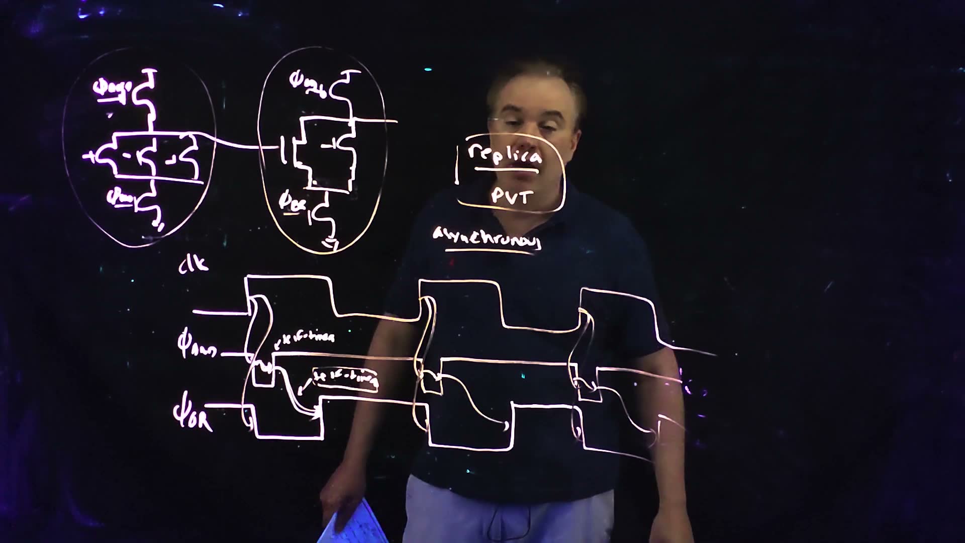
Fair copy of the board above (Lecture17 @ 43:07), mark for mark in its own layout. One pale pen drew the whole board (the edge light tints it violet at the left and peach at the right), copied in black. The clock labels marked † are written over the “clk” labels of the first drawing (37:47); they read φAND and φOR, and the leftover strokes of “clk” are left out. The precharge devices are copied as drawn: the AND row’s without a bubble, the OR column’s with the bubble of its first gate lead. As on the board, φOR falls at clk’s rising edge together with φAND; the generator of Section 9 makes it fall a replica precharge later, as the redraw above shows. The waveforms are set level (on the board they drift down to the right), and the last clk fall trails off as drawn. The lecturer stands behind the waveforms, which show over him: nothing is restored (41:41 and 44:03 show the same strokes).
Self-timing is asynchronous
board (42:06–43:07; the board writes “asynchronous” and underlines it). The numbers for these edges come in Section 9’s worked example: φAND low from 30 to 220 ps and φOR from 200 to 440 ps, with example delays. “This is an asynchronous technique, because in synchronous design … the only thing that triggers anything is the clock” (42:10–42:41). Here a signal edge (the replica finishing) triggers a clock edge, and the delays involved “have nothing to do with the clock”. That is what lets the edges track the circuit, and it is also the risk: nothing is checked against a clock period, so the replica must be verified at every PVT corner.
φOR’s falling edge added is a replica’s too: a replica precharge after φAND falls, as the figure’s caption says (the board draws it at clk↑).
Memorize or derive. Derive the edges from the generators, as Section 9 does; what to memorize is which edge belongs to the clock (only φAND’s fall) and which to a replica (the other three).
Traps.
- φAND as a delayed copy of clk. Only its rising edge waits; it falls at once, the shape of Chapter 14’s chopper.
- A replica of a typical row. It must copy the slowest row, or the real rows fail at some corner.
- A fixed delay instead of a replica. An inverter chain tuned at one corner need not track the rows’ capacitance and devices at another.
Check yourself Which edges of φAND and φOR are set by the clock, and which by a replica?
Only φAND’s falling edge is the clock’s (clk rising, through the NAND). φAND’s rise waits for a replica’s precharge, φOR’s rise for a replica’s evaluate, and φOR’s fall for a replica’s precharge after φAND falls.
Check yourself The chip runs hot and every circuit delay grows. What happens to φAND's low pulse if it is made by a replica row, and if it is made by a fixed inverter chain that matched the rows at room temperature?
With a replica, the pulse grows with the replica’s precharge, which grows like the real rows’ (same devices, same layout, same capacitance), so the rows still finish precharging. With an inverter chain, the pulse grows with the inverters, whose delay need not scale like a row’s precharge through its PFET and wire; if the rows slow down more, the pulse ends before they are precharged, and requirement 1 fails.
9. Generating φAND and φOR with replica rows
You need
A NAND is 0 only when both inputs are 1. An inverter, or a bubble at a gate input, flips its signal after a delay .
A dynamic row clocked by a signal (Section 7). While is low it precharges, rising after ; when rises it evaluates, falling after if any of its devices is on. The slowest precharge is the row with the most capacitance; the slowest evaluate is a row with only one device on.
The edges to produce (Section 8): φAND falls at clk↑ and rises a replica precharge later; φOR rises a replica evaluate after φAND rises.
The question. What circuits make these edges? The lecture draws two, and FN19-6b prints the same two and asks for the replica row inside them.
The φAND generator
board (43:41–45:31). clk goes straight to one input of a NAND. It also goes through an inverter to a dummy AND row (the board’s name; a replica), clocked by . The dummy row’s output enters the NAND’s other input through a bubble. The NAND’s output is φAND.
The φAND generator, redrawn from the board (Lecture17 @ 50:10; FN19-6b prints the same circuit). Top: clk into a NAND directly, and through an inverter into the dummy row (clocked by ), whose output enters the NAND through a bubble. Bottom added: clk, φAND, and , with the worked example’s delays in proportion. When clk rises the NAND falls (φAND↓); precharges on low, and once it is high the bubbled input drops and φAND rises ().
The board (Lecture17 @ 50:10)
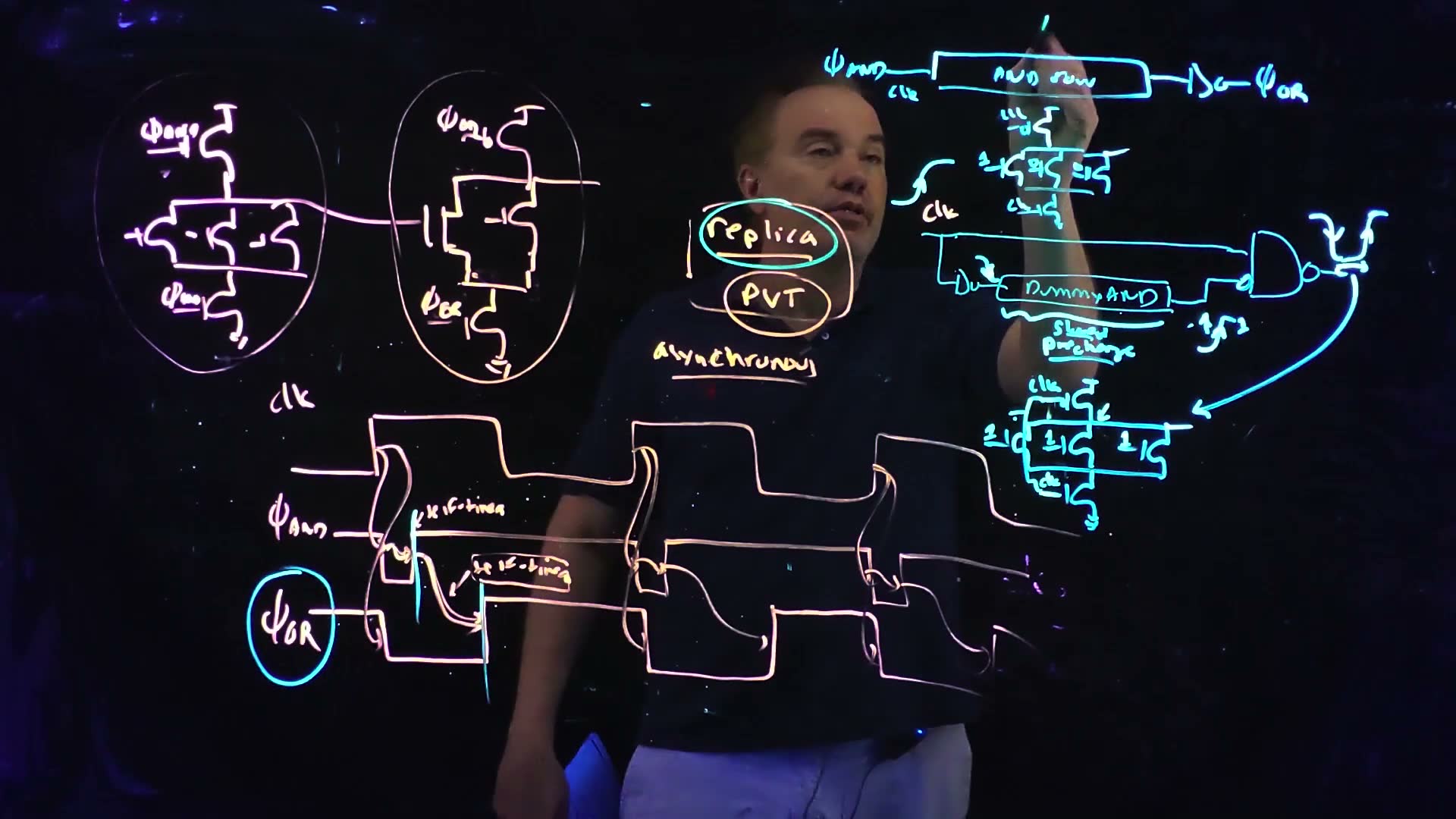
Fair copy of the board above (Lecture17 @ 50:10), mark for mark in its own layout. Black is the pale pen: the 43:07 board, as in its fair copy, with the ring now drawn round PVT. Teal is the cyan pen: the rings on “replica” and φOR, two marks through the waveforms at the first rising edges of φAND and φOR, and both generators. At the top, the φOR generator: φAND through an AND row clocked by clk and an inverter, with that row’s dummy (gates 1, 0, 0). Below it, the φAND generator, with clk into a NAND directly and through an inverter to “Dummy AND” (“Slowest precharge”), and the dummy row it points to (gates 1, 1, 1). The middle of the “AND row” box and the upper dummy row are under the lecturer’s hand here and are copied from 49:25. That row’s middle gate digit is written over (†); the speech (49:09, “set only one of these to a one”) makes it 0. The small mark under the NAND’s input is copied as drawn; it is not read in the lecture. The board’s inverters, drawn as small D shapes, are set as triangles.
The NAND-and-replica generator, one cycle (board, 44:20–45:31)
- Before clk rises. clk has been low, so is high and the dummy row has evaluated: its inputs are on, so is low and the bubbled NAND input is 1. With clk = 0 the NAND’s output, φAND, is 1.
- clk rises. Both NAND inputs are now 1, so φAND falls one NAND delay later: the AND plane starts to precharge.
- The replica precharges. falls one inverter delay after clk rose, and the dummy row starts to precharge. When is high, the bubbled input drops to 0.
- φAND rises. One NAND delay after that, φAND rises and the AND plane evaluates. Its low pulse lasted as long as the replica took to precharge, plus the two gate delays around it.
- clk falls. The NAND sees clk = 0 and stays high. rises, and the dummy row evaluates again, back to low, ready for the next rising edge.
The dummy rows
board (45:33–47:36). The dummy row is a real AND row, laid out like the others, with as many NFETs as any row can have: the maximum literal count, 3 in the example, since a product holds at most one of and for each input (46:11). In the φAND generator all three gates are tied to 1. With every device on, the node between the devices and the foot is joined to the row and must be charged too: “that’s going to produce the maximum amount of capacitance on this node, which is going to give me the slowest precharge” (46:37).
The two dummy rows, redrawn from the board (Lecture17 @ 49:25; the board writes the generic “clk” on each row’s precharge device and foot, and the labels here are the clocks each generator feeds it). Left, in the φAND generator, clocked by : all three gates at 1, so every device is on and the internal node between the devices and the foot is charged with the row: the slowest precharge. Right, in the φOR generator, clocked by φAND: one gate at 1 and two at 0, so it discharges through a single device: the slowest evaluate.
The φOR generator
board (47:38–49:37). φAND clocks a second dummy row; its output , inverted, is φOR.
The φOR generator, redrawn from the board (Lecture17 @ 49:25). Top: φAND clocks the dummy row , and an inverter after it gives φOR. Bottom added: its waveforms with the worked example’s delays. φAND falling starts ‘s precharge, so φOR falls a precharge later (); φAND rising starts ‘s evaluate through its one on device, so φOR rises only after the slowest evaluate ().
The replica-and-inverter generator, edge by edge (board, 47:38–49:37)
- φAND falls. precharges; when it is high, φOR falls (one inverter later) and the OR plane precharges.
- φAND rises. The real AND rows start to evaluate, and so does . Its gates are 1, 0, 0: “I’m gonna set one of these to a one because the slowest evaluation is gonna be when only one of these evaluates” (49:09–49:37). A row discharging through one device is the slowest any real row can be.
- φOR rises one inverter after is low: by then every real row has settled, so the OR plane evaluates on final rows. Requirement 2 holds at every corner, because is a real row.
A replica has the same structure, the same layout, and sits in the same place (a dummy row inside the PLA’s own array, 50:02–50:28). “This is very commonly done in SRAMs … lots of features in SRAMs are also going to be self-timed” (50:28).
A worked example: timing the two clocks
added Example delays, for example: ps, ps, the replica’s precharge ps, its evaluate through one device ps, the OR plane’s evaluate 150 ps, and an output latch that needs 50 ps of setup. clk rises at 0.
The two clocks timed with the example delays added, computed from , , , ps, an OR-plane evaluate of 150 ps and a 50 ps setup, clk rising at 0. φAND is low from 30 to 220 ps (190 ps), φOR from 200 to 440 ps (240 ps), the outputs are valid at 590 ps (after the OR plane’s 150 ps evaluate), and with the 50 ps setup the period must be at least 640 ps. The clock is drawn rising again at 800 ps.
Edge by edge
- φAND falls one NAND delay after clk rises: at 30 ps.
- φAND rises after the inverter, the replica’s precharge, the bubble and the NAND: 220 ps. It was low for 190 ps, which is : more than ps, so requirement 1 holds for the AND plane, with the two inverter delays to spare.
- φOR falls when has precharged after φAND fell, then the inverter: 200 ps.
- φOR rises when has evaluated after φAND rose, then the inverter: 440 ps. The slowest real row finished at ps, so requirement 2 holds, by one inverter delay.
- The OR plane’s precharge window. φOR is low from 200 to 440 ps, 240 ps. It must cover the OR plane’s precharge.
- The outputs are valid after the OR plane’s evaluate, at 590 ps, and the output latch needs them 50 ps before the next clk edge: the period must be at least 640 ps.
Check by the closed form: the OR window is ps, the same as step 5. Two conditions on clk itself: its high phase must outlast φAND’s low pulse (here 190 ps; at a 640 ps period with a 50 % duty, the high phase is 320 ps), or clk’s fall would end the pulse early; and its low phase must let the dummy row evaluate again before the next rising edge.
Memorize or derive. Derive, three lines: (1) clk↑ → φAND↓ after ; (2) clk↑ → ↓ () → high () → bubble low () → φAND↑ (), so the low time is ; (3) φOR follows φAND’s edges through and one inverter, a precharge after the fall and an evaluate after the rise.
After the outputs are taken added. From about after each clk↑ until φOR falls (30 to 200 ps here), the rows precharge high while the OR plane still evaluates, so the previous cycle’s outputs may be lost soon after the edge that captures them. That is harmless if they are captured at that edge with the latch’s hold time met.
One replica design for both generators
FN19-6b asks for “a replica AND row, two instance of which can be used in the circuits below to generate and ” (FN19, p14): one design, used twice. The lecture’s two rows differ (all on for φAND, one on for φOR). A single design that serves both added:
A single replica row (added)
- Copy a real AND row, laid out like the others in the array, with its own precharge PFET and foot driven by the replica’s clock input.
- Give it the maximum literal count of NFETs (3 here), so that its row node carries every device’s drain capacitance.
- Tie one NFET’s gate to and the others to ground. In the φOR generator it then evaluates through one device: the slowest evaluate. In the φAND generator it still precharges the internal node, through the one on device, so its precharge is at least as slow as the all-on row’s: the slowest precharge.
- Load its output like a real row’s: the same wire and the same OR-plane gate capacitance, so that its delays are the real rows’.
- The cost: in the φAND generator this row evaluates through one device too, so clk’s low phase must cover : the inverter to , the row’s evaluate and the NAND’s bubble, before the bubbled input is back at 1 for the next rising edge (240 ps with the example delays; the low phase is 320 ps at a 640 ps period).
The datapath practice page (FD1) solves FN19-6b in full; the lecture’s two rows are an equally valid, more conservative answer.
Traps.
- The typical literal count in the precharge replica. A row with fewer devices precharges faster, so the real rows with three are cut short.
- All inputs on in the evaluate replica. Three parallel devices discharge fastest; the slowest real row has one on.
- A dummy row that is not discharged before clk rises. The bubbled input is then 0 and the NAND never falls.
- Reading the φAND generator as a delayed clock. It is a chopper (Chapter 14 §5) whose delay is a replica.
Check yourself The widest product of a PLA has 5 literals. How many NFETs does each of the lecture's dummy rows get, and how many of them are on?
Five each (the maximum literal count). The φAND row has all 5 on (the slowest precharge); the φOR row has 1 on (the slowest evaluate).
Check yourself With the worked example's delays, only tpre changes, to 250 ps. When does φAND rise, how long is it low, and when does φOR rise?
φAND still falls at 30 ps and is low for ps, so it rises at ps. φOR rises ps later, at 540 ps.
10. SRAM organization: rows, columns and address bits
You need
Binary addressing added. address bits select one of things, so selecting one of (a power of two) takes bits: 10 bits for 1024.
A multiplexer (Chapter 10 §7): select bits choose one of inputs and pass it to the output.
The question. The third kind of block is the array. What is inside an SRAM, how is a memory of so many words of so many bits laid out as a grid, and which address bits go where?
SRAM and DRAM
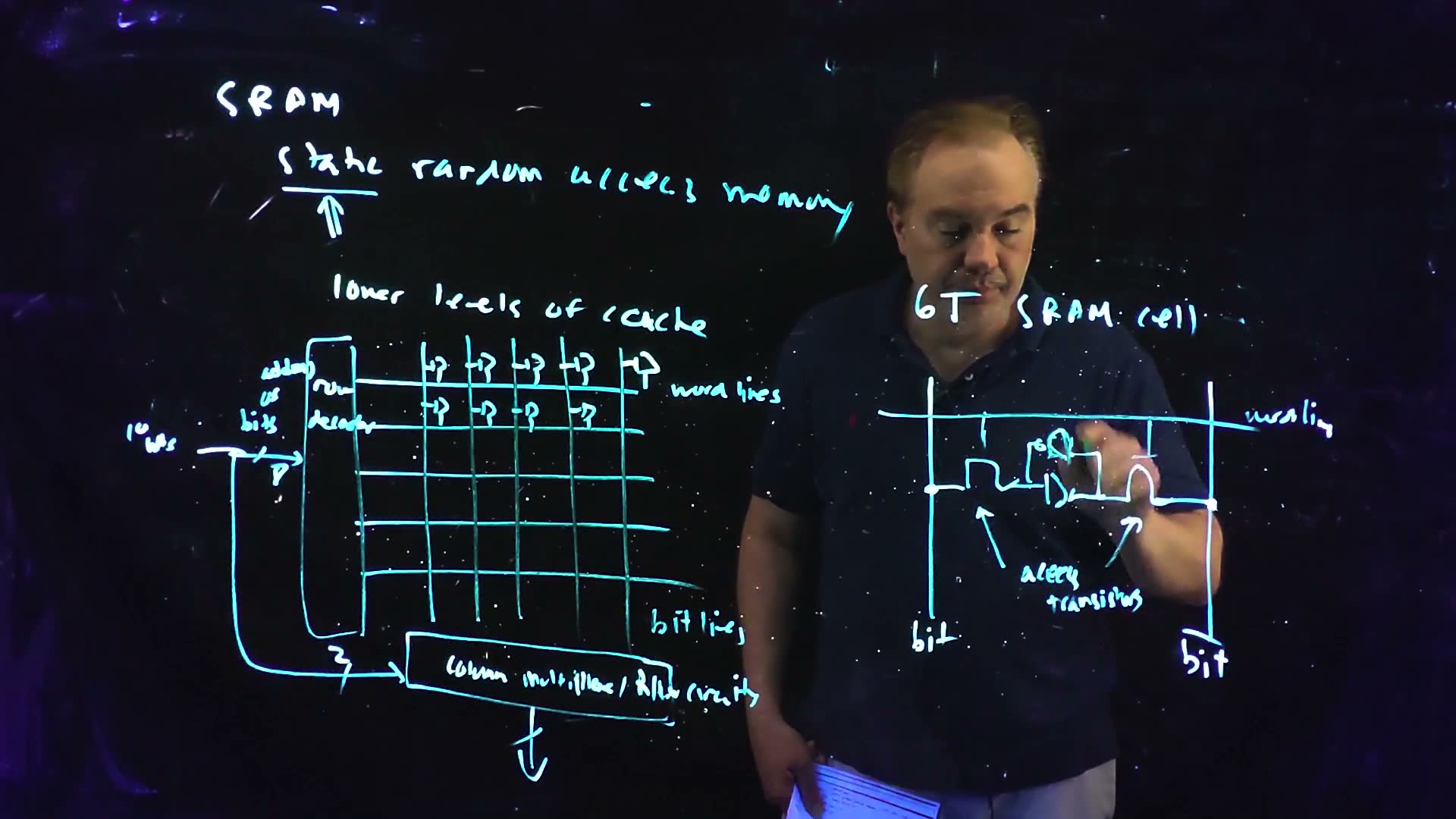
board (51:53–53:51; the board writes “SRAM, static random access memory” and “lower levels of cache”). An SRAM keeps its data as long as the power is on. A DRAM forgets: each cell must be read and written back (refreshed) within its retention time, by a DRAM controller. Level-one caches are almost always SRAM, and level-two caches often.
The array
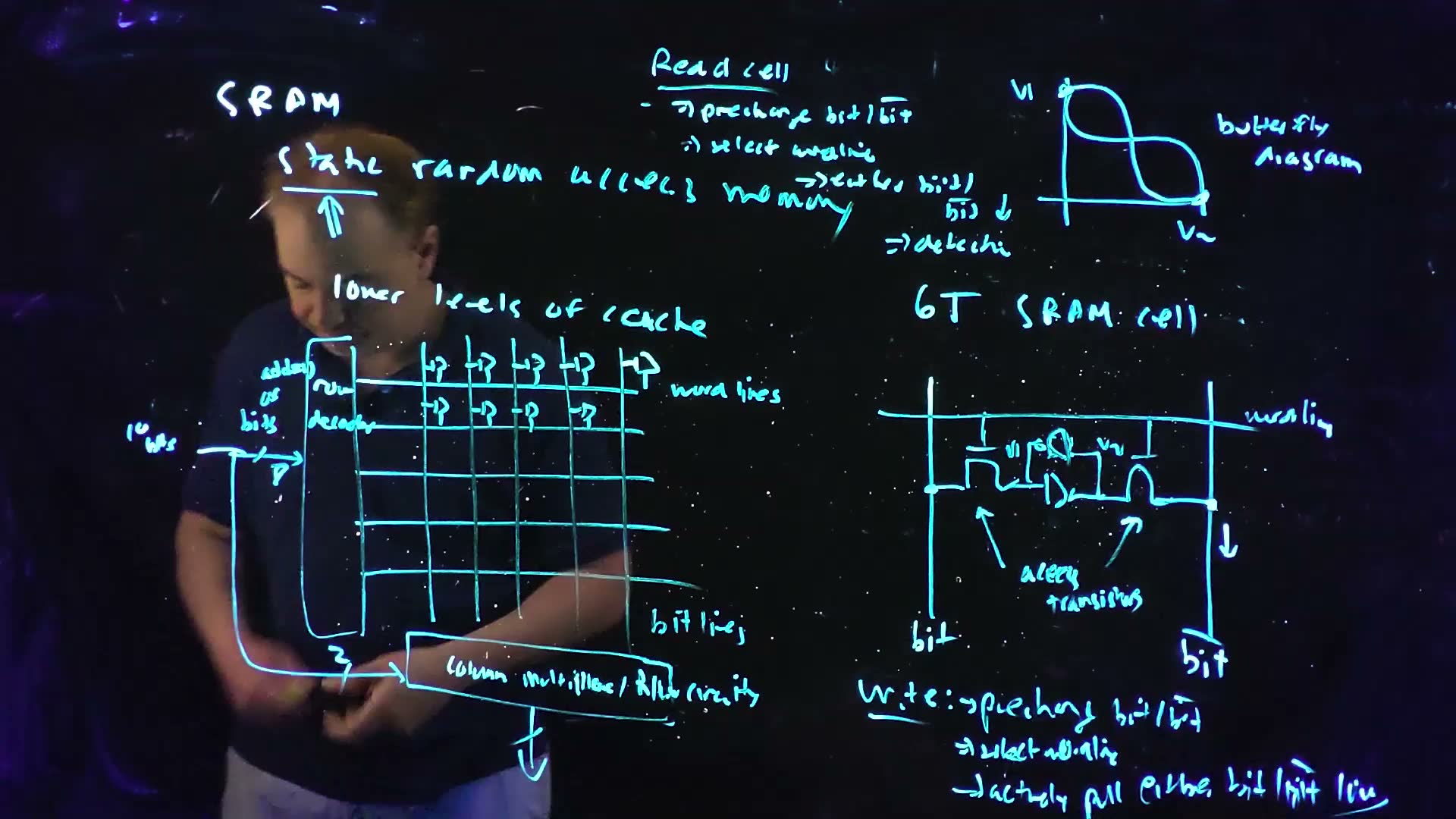
board (54:08–57:57). Horizontal word lines (rows) come from a row decoder, which raises one of them for each address. Vertical bit lines (columns) cross them, and a memory cell sits at every crossing, attached to both (57:47). At the bottom, a column multiplexer with the read/write circuitry picks out the bits of one word.
The SRAM array, redrawn from the board (Lecture17 @ 57:57; the cells at every crossing as at 59:32, where the board completes them). Ten address bits split: 8 go to the row decoder (left, unlabelled), which raises one of 256 word lines (WL), and 2 to the column multiplexer and read/write circuits (mux / R/W), which pick one of the four 32-bit words on the selected row’s 128 columns (bit-line pairs, BL). The numbers 256 and 128 are this chapter’s example; the board leaves the grid unnumbered.
The board (Lecture17 @ 57:57)

Fair copy of the board above (Lecture17 @ 57:57), mark for mark in its own layout. Black is the cyan pen; orange is the cream pen with which the lecturer is drawing the memory cells: two cell marks at the top row’s rightmost crossings, the only ones drawn so far (the board has a cell at every crossing by 59:32). The lecturer’s hand washes out the grid’s top right corner here; the lines there are read on 57:35. The three stacked words at the decoder’s left read “address bits”. The text lines are set level; the grid lines, the bus and the multiplexer box keep their drawn slopes.
Logical and physical organization
The board's example (55:45–57:22)
- Logical organization. A memory of 1024 words of 32 bits, written 1024 × 32, is what the user sees: give an address, get 32 bits. Selecting one of 1024 words takes address bits.
- Built as it reads? added 1024 rows of 32 cells is a strip 32 times taller than wide: long bit lines, a huge decoder.
- Fold it. added The same 32,768 cells as 512 rows × 64 columns put two words on each row: 9 address bits pick the row and 1 bit picks one of the two words, through a 2:1 column multiplexer.
- Fold again. 256 × 128 puts four words on a row: 8 bits pick one of 256 rows, and the other 2 bits drive a 4:1 column multiplexer that takes “128 bits down to my 32 bits”. “Because I can do column multiplexing, I can do whatever physical organization makes the most sense” (57:22).
One logical organization, three physical ones added (the values are the board’s, Lecture17 @ 57:57). Each rectangle holds the same 32,768 cells, drawn to scale. 1024 × 32 (the logical shape, 10 row bits, no column multiplexer), 512 × 64 (9 row bits, 1 column bit, 2:1) and 256 × 128 (8 row bits, 2 column bits, 4:1).
Memorize or derive. Memorize address bits (the board’s example). Derive the split: each row holds words, so the column bits choose one of , and the row bits one of rows; since , the two add up to .
Worked examples
Two splits
- The board’s: 1024 × 32 as 256 × 128. address bits. Rows: . Words per row: , a 4:1 multiplexer, column bits. Check: .
- Added: 2k × 8 as 128 × 128. 2k = 2048 words, address bits. Rows: . Words per row: , a 16:1 multiplexer, 4 column bits. Check: , and cells.
On a past final (FN10-10). The same two moves: a 4k × 16 memory needs address bits, and built as 256 × 256 it uses row bits and a :1 column multiplexer, 4 column bits (). The memory practice page (FM1) solves both parts; Chapter 19 draws the column multiplexer’s circuit.
What sits at each crossing (57:47–58:21). The cell is the 6T SRAM cell, attached to its word line and to a pair of bit lines, bit and . Chapter 19 opens it: two cross-coupled inverters and two access transistors, read stability, writability and the butterfly. The lecture’s boards from 59:32 on are in this chapter’s board gallery, at the end of the page.
One cell at a crossing added (the lecture’s words at 57:47; the bit and pair from 59:52). Each cell connects to its row’s word line (WL) and to its column’s pair of bit lines. What is inside the box is Chapter 19’s.
Traps.
- Column bits as . The multiplexer chooses words, not bits: for 256 × 128 with 32-bit words it is , not .
- The logical shape as the physical one. 1024 × 32 built as it reads is 32 times taller than wide; designers fold the array toward a square with column multiplexing.
Check yourself A memory is 2k × 32. How many address bits does it need?
2k = 2048 words, 11 bits. The word width does not enter.
Check yourself The same 2k × 32 memory is built as 512 × 128. How many address bits go to the row decoder, how many to the column multiplexer, and what is the multiplexer's ratio?
Rows: 9. Words per row: , a 4:1 multiplexer, 2 column bits. Check: , and cells.
On the exam
The past finals test this chapter in three questions: two PLAs to read, a replica row to design, and a memory’s address bits. 37 points in all.
| Part | Points | What it asks | Sections |
|---|---|---|---|
| FN12-10a | 9 | the functions , of a static PLA: the example’s first three rows, output inverters drawn | §2, §3, §4 |
| FN19-6a | 10 | the functions , of a dynamic PLA with correct clocks: the example’s four rows, no output inverters | §3, §4, §7 |
| FN19-6b | 8 | a replica AND row, used twice, to generate φAND and φOR | §8, §9 |
| FN10-10a | 4 | the address bits of a 4k × 16 memory | §10 |
| FN10-10b | 6 | the column-multiplexing bits when it is built as 256 × 256 | §10 (Chapter 19 draws the multiplexer) |
| FN12-10d | 9 | a ROM: a full decoder into a pseudo-NMOS NOR plane, read without inverters | §2–§4, as context (Chapter 19) |
FN12-10a and FN19-6 are solved on the datapath practice page (FD1), FN10-10 on the memory practice page (FM1). At the finals’ pace of 0.7–0.9 minutes a point, FN19-6 is a 13–16 minute question.
Memorize.
- A product is the NOR of its literals’ complements, so a true literal’s device sits on the complement line; a column is the NOR of its rows.
- Look for the output inverters before writing a PLA’s outputs: without them, each output is the complement of its sum.
- Espresso’s codes: 1 = true, 0 = complemented, – = absent; in the output part, 1 = the output uses the product. Rows = distinct products.
- Each plane precharges while its clock is low. The two requirements: φAND’s low pulse at least the slowest row’s precharge; φOR rises only after the slowest row’s evaluate.
- The replica rows: the maximum literal count; all on for the slowest precharge (φAND), one on for the slowest evaluate (φOR); one design with one on serves both.
- Address bits ; row bits ; column bits .
Derive (with the path).
- NOR–NOR from AND–OR: an OR is a NOR and an inverter; an AND is a NOR of complements (De Morgan).
- A row’s function from its devices: flip each device line’s literal, AND them.
- The generators’ edges: clk↑ → φAND↓; ↓ → precharged → bubble → φAND↑, so ; φOR↑ a after φAND↑; the OR window .
Method cards. FN19-6b belongs to the clock-generation card (its move 8, a replica delay, points here). The playbook’s PLA card (recognize a grid with pull-ups at the row ends and the column tops; moves: rows, columns, inverter, simplify, check two rows; traps: the gate’s line, the missing inverter) covers FN12-10a and FN19-6a.
The lecture’s boards
The boards of Lectures 16 and 17 used in this chapter (23 frames)