2. Semiconductor basics
Lecture 2 lays the ground for every device in the course. It starts with the material, silicon, and explains with a band picture why pure silicon barely conducts. Then come the two properties that make a semiconductor useful: its conductivity rises steeply with temperature, and a tiny amount of doping changes it by orders of magnitude. The Fermi level ties these together: one number that tells you how many electrons and holes there are. The lecture ends by making a pn junction, the first real device, and explaining why it lets current through in only one direction.
After this chapter you can:
- describe silicon’s crystal, its atom density and the centimetre-based units of device physics;
- explain how bands and the band gap form as atoms come together, and why silicon at is an insulator;
- state the two properties that make a semiconductor, and calculate electron and hole concentrations in intrinsic and doped silicon with ;
- use the Fermi–Dirac function and to find the Fermi level from the doping, and the reverse;
- outline how a pn junction is made: oxidation, lithography, etching, implantation, annealing and contacts;
- explain in words and band diagrams why a pn junction forms a depletion region and a barrier, and why it conducts in forward bias but only leaks in reverse.
Boxes and equations marked board were written in the lecture. Parts marked added are explanations or examples this guide adds.
Before you start
You need a few ideas from Chapter 0. Each is restated here so you don’t have to flip back.
- Energy and voltage. An electron volt (eV) is the energy an electron gains across one volt. Energies in this chapter are in eV; dividing by turns them into volts with the same number.
- Logarithms. If then . Each factor of 10 is , so at room temperature : 60 meV per decade.
- Band diagrams. Energy is up, position is across. An electron is lower in energy at a higher potential, so bands bend opposite to the potential.
- Constants in cm units: (and ) at 300 K, , for silicon.
Notation. and are the electron and hole concentrations, in . and are the donor and acceptor concentrations. and are the conduction- and valence-band edges, the intrinsic Fermi level and the Fermi level. As on the board, the chapter writes the thermal energy in the exponents; the worked examples use .
1. Silicon, the material
The idea. Silicon is a single element from group IV. Every atom bonds to four neighbours, and there are about atoms in each cubic centimetre.
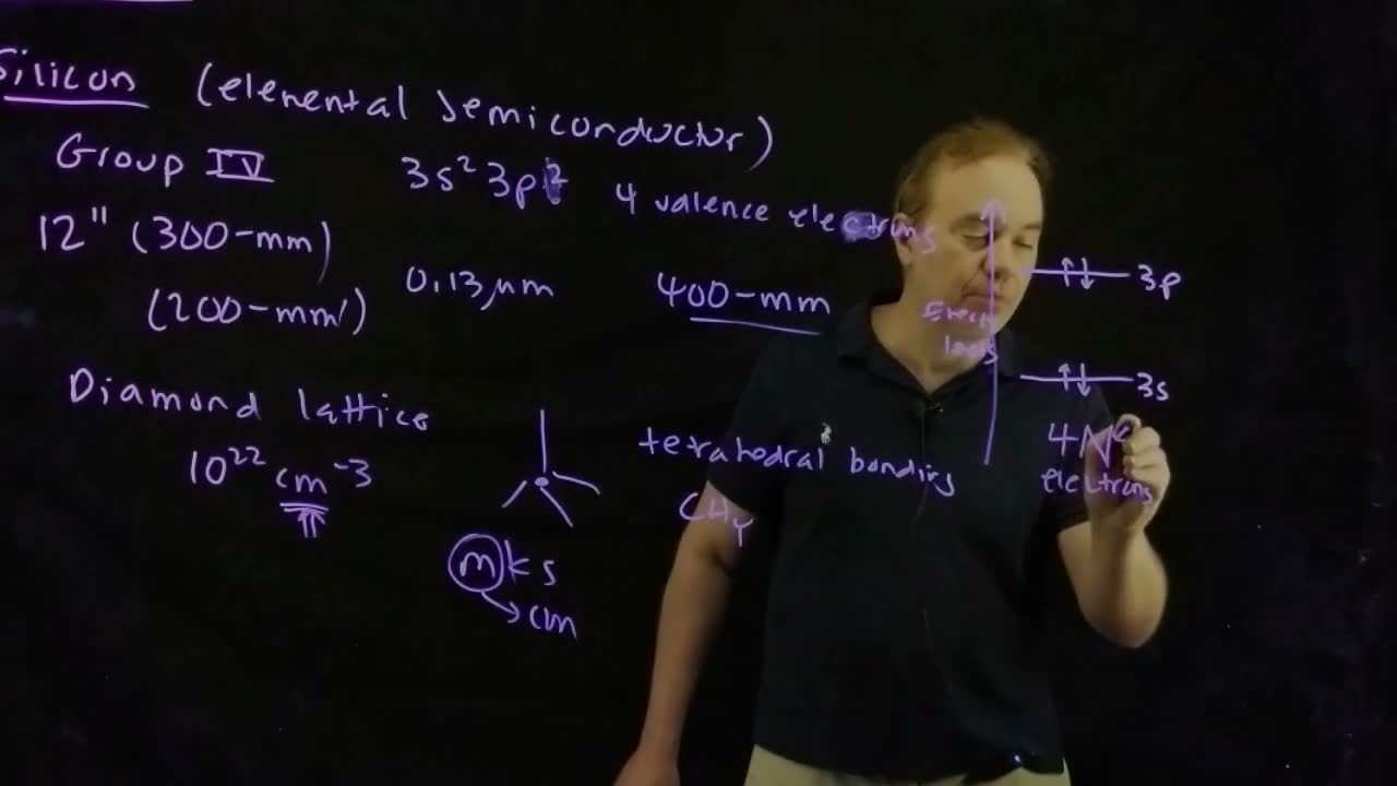
- An elemental semiconductor (0:48). Silicon sits in group IV of the periodic table. A compound semiconductor such as gallium arsenide needs two elements; silicon needs only one.
- Boules and wafers (1:07). Silicon is grown as a single crystal, a long cylinder called a boule, and sliced into wafers. Today’s wafers are 300 mm (12 inches) across; the older size is 200 mm (8 inches). The change happened at about the 0.13 µm technology node: at 0.13 µm you find both, and every node after it is 300 mm. A move to 400 mm has been discussed, with some tooling built, but it has not reached major production (1:33).
- The diamond lattice (2:16). Each silicon atom bonds to four others in a tetrahedral arrangement, the same shape as the bonds of methane, CH₄. A whole crystal built this way is the diamond lattice; carbon in the same structure is diamond. The crystal holds about atoms per cm³ (2:55). (The precise value is added; the lecture’s round is used below.)
- Four valence electrons (4:17). The outer shell is : two electrons in the 3s orbital and two in the 3p orbitals. The lecturer first says , corrects himself, and the board shows the 6 overwritten with a 2.
The units of device physics
The lecture’s units are MKS, except that the metre is replaced by the centimetre (3:23). It isn’t CGS: charge is still in coulombs, voltage in volts. Concentrations are per cm³, fields in V/cm, capacitances per area in F/cm². The lecturer calls this a legacy of Shockley, kept in the United States; in Europe you will see straight MKS, with concentrations per m³.
Worked example. added Convert a doping of to .
- One metre is 100 cm, so one cubic metre is cubic centimetres.
- A cubic metre therefore holds times as many atoms: .
Check yourself How many valence electrons does a silicon atom have, and why does the number matter for doping?
Four (), because silicon is in group IV. Replacing a silicon atom by a group V atom adds a fifth electron; a group III atom brings one too few. Section 4 builds doping on exactly this count.
2. From atomic levels to bands
The idea. Bring many silicon atoms together and their sharp atomic energy levels spread into two bands of allowed energies, separated by a band gap with no states at all.
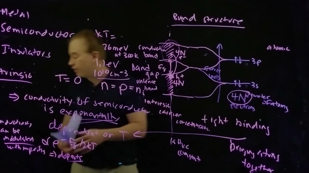
The lecture builds the bands with the tight-binding picture (7:06): start from isolated atoms and imagine pushing them together.
Bands from atomic levels (board, 4:59–9:55)
- Isolated atoms. Each silicon atom has a 3s level and a 3p level. Its four valence electrons fill the 3s level (two, spin up and down) and two of the six 3p places. With atoms there are electrons.
- Count the places. Each atom offers 2 places in 3s and 6 in 3p, so atoms offer places (9:26). When the atoms are far apart, all copies of a level sit at the same energy: the level is hugely degenerate (about copies per cm³).
- Bring the atoms together. The orbitals of neighbouring atoms start to overlap and interact. The degeneracy is lifted: each level spreads into a range of closely spaced energies (8:05).
- At the real spacing, the lattice constant of silicon, the levels have regrouped into two bands (8:43): a lower valence band and an upper conduction band.
- Share out the places. The states split evenly: in the valence band and in the conduction band (9:26).
- The gap. Between the top of the valence band and the bottom of the conduction band is an energy range with no states at all, the band gap board: in silicon (9:16).
What happens at absolute zero (9:55). There are electrons and exactly valence-band states. At every valence state is filled and every conduction state is empty. An electron can only move if it has an empty state to move into, and there is none nearby. So at silicon has no free carriers: it is a perfect insulator (10:31).
Common mistakes.
- Treating the band gap as a physical gap in the crystal. It is a range of energies with no allowed states, not a region of space.
- Thinking a full band conducts because it has many electrons. A completely full band carries no current: no electron has an empty state to move into.
Check yourself Silicon has 4N valence electrons and 8N states. Why is it an insulator at T = 0 rather than a conductor?
Because the states split into two bands of , and the electrons exactly fill the lower one. A full band has no empty states, and the empty band sits higher, across the gap. With nothing to move into, no electron can respond to a field.
3. What makes a semiconductor, part 1: temperature
The idea. Heat lifts a few electrons across the gap. Each one leaves a hole behind, and both can carry current, so conductivity rises exponentially with temperature.
A semiconductor sits between metals, which conduct a lot, and insulators, which don’t conduct at all (10:50). But “somewhere in between” is too simple a definition. The lecture names two characteristics, and the first is this (11:28):
Why. At any temperature above zero, there is a chance that an electron in the valence band is excited into the conduction band (12:08). That creates an electron–hole pair (12:48):
- the electron is now in the nearly empty conduction band, with plenty of empty states to move into;
- the empty state it left in the valence band is a hole (). Like a bubble in a liquid, the hole moves too, and it behaves as a positive charge.
Both are free carriers. The higher the temperature, the more pairs are generated, and the conductivity grows exponentially.
Intrinsic silicon (13:21). In perfectly pure silicon every electron excited into the conduction band leaves exactly one hole. So
where is the intrinsic carrier concentration, at room temperature board (14:03).
Where the ½ in the exponent comes from. added The lecture writes but doesn’t stop on the 2. Section 6 supplies the reason: in intrinsic silicon the Fermi level sits in the middle of the gap, so the conduction band is only above it, and the chance of finding an electron there falls as .
Worked example. added By what factor does grow when silicon warms from 300 K to 310 K? Use .
- The ratio of the two factors is .
- .
- .
- The exponent is , and .
- A 10 K rise roughly doubles the intrinsic carrier population. That is what “exponentially dependent on temperature” means in practice.
Common mistakes.
- Mixing up and . is an energy; is a voltage. They have the same number.
- Reading as a constant. It is the room-temperature value; it rises steeply with temperature.
Check yourself In intrinsic silicon, why must n equal p exactly?
Every carrier comes from one thermal event that lifts one electron out of the valence band. Each event makes one conduction electron and one hole, so the two counts are always equal.
4. What makes a semiconductor, part 2: doping
The idea. Replace one silicon atom in ten million by phosphorus and the electron concentration jumps from to . A tiny amount of the right impurity changes the conductivity by orders of magnitude.
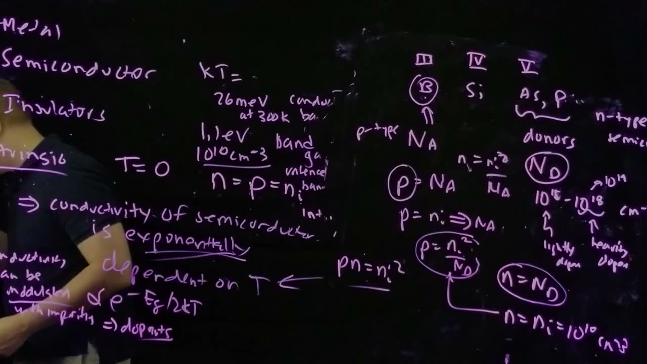
The lecturer calls this “the more important second characteristic” and “by far the most interesting” (14:18): the conductivity can be modulated, by many orders of magnitude, with a very small number of impurities. The impurities are called dopants, and they must be special ones.
Donors: n-type silicon
Look at the columns either side of silicon in the periodic table (16:20). Arsenic and phosphorus are in group V. Put one in place of a silicon atom and that site has five valence electrons instead of four. The extra electron goes straight into the conduction band and conducts (16:54). These dopants are donors, with concentration . Each donor adds one electron, so
How much doping? (17:39) A typical range is (lightly doped) to (heavily doped), and in some cases up to about board.
Why so few dopants matter so much (18:02–19:33)
- Silicon has about atoms per cm³.
- Heavy doping, , replaces one atom in . Even the heaviest doping is a small impurity.
- Light doping, , replaces one atom in .
- Yet it raises the electron concentration from to : five orders of magnitude more electrons, and so far more conductive.
Acceptors: p-type silicon
Boron is in group III (19:33). In place of silicon it brings one valence electron too few. It accepts an electron from the valence band, which creates a hole. These dopants are acceptors, with concentration , and everything works the same way with holes:
The mass-action law
In thermal equilibrium the product of the electron and hole concentrations is fixed (20:53):
So raising one carrier concentration by doping lowers the other (21:20). In n-type material, and the holes drop to
In p-type material, and board.
Majority and minority carriers (22:31). In n-type silicon electrons vastly outnumber holes: electrons are the majority carriers, holes the minority carriers. In p-type silicon the roles swap.
Worked example. The lecture’s own (21:53): .
- Majority carriers: .
- Minority carriers: .
- Check: . ✓
- Electrons outnumber holes by : ten orders of magnitude. The lecture says “five orders of magnitude more electrons than holes” here (22:08), a slip; five orders is how far rose from , and fell by the same five orders.
Worked example. added A p-type body with , the doping Chapter 3 uses for the MOS capacitor.
- Majority carriers: .
- Minority carriers: .
- About one thousand electrons per cm³, against holes.
Common mistakes.
- Forgetting the minority carriers fall. Doping doesn’t just add majority carriers; through it suppresses the other type.
- Using when is not much larger than . The simple rule needs ; near the thermal pairs count too.
- Reading the carrier ratio as an exact conductivity ratio. added Conductivity also depends on how easily the carriers move, their mobility, which Chapter 4 introduces.
Check yourself NA = 1016 cm−3. What are the majority and minority carrier concentrations?
Holes are the majority: . Electrons are the minority: .
5. The band diagram
The idea. Throw away the details of the band structure and keep only its two edges, and , drawn against position in the device.
The tight-binding picture of Section 2 plots energy against atomic spacing. For devices the lecture abstracts it (25:04):
- keep only the band edges: , the bottom of the conduction band, and , the top of the valence band;
- plot them against position through the device.
For a uniform piece of semiconductor nothing changes with position, so the bands are flat (25:16). Electrons live just above , holes just below . Later, bands that are not flat will mean an electric field (Section 9).
6. The Fermi–Dirac function
The idea. One smooth step function gives the probability that a state at energy holds an electron. Temperature sets how smooth the step is; doping sets where it sits.
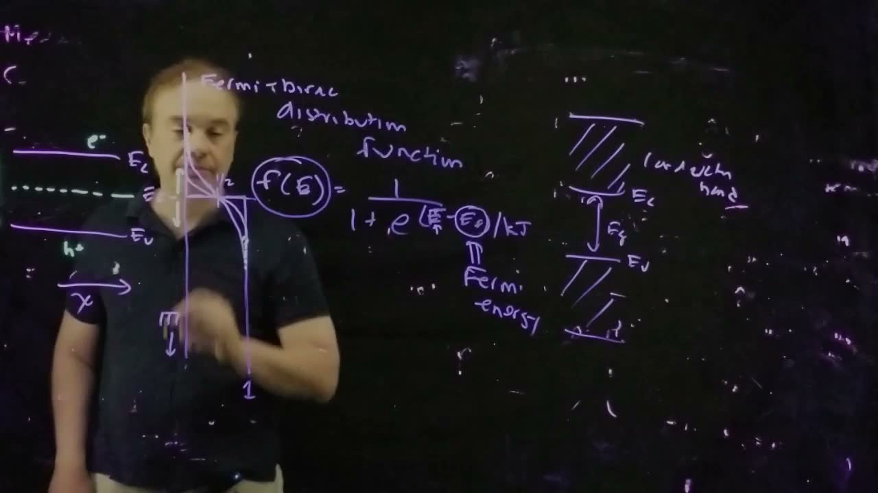
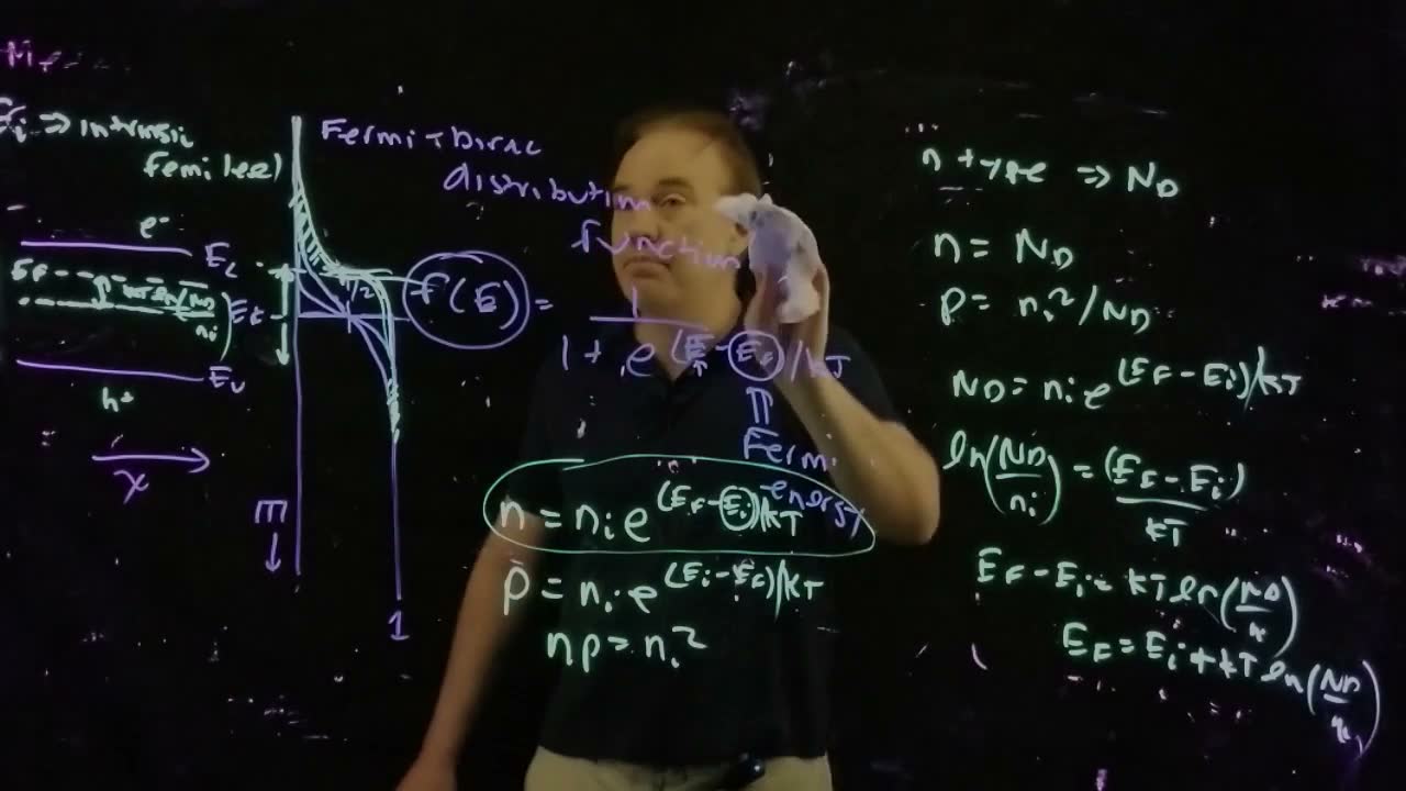
Electrons are fermions: no two can occupy the same state. In thermal equilibrium they fill the available states according to the Fermi–Dirac distribution function (26:38), a sigmoid:
Reading the function (27:40–28:36)
- At it is a sharp step: for every state below (all full) and for every state above it (all empty).
- At the exponent is zero, so . At any temperature, a state at the Fermi level is half likely to be full.
- As the temperature rises the step smooths out over a range of a few on each side of . Its midpoint stays at .
The board draws sideways, with energy upward and running from 0 to 1, so that it lines up with the band diagram beside it.
The tails make the carriers (29:18). Put in the middle of the gap and warm the crystal:
- just below , the curve dips slightly below 1. A state there has a small chance of being empty: that’s a hole;
- just above , the curve rises slightly above 0. A state there has a small chance of being full: that’s an electron.
With at mid-gap the two tails are symmetric, so there are as many electrons as holes: (29:44). Raise the temperature and both tails grow: goes up (30:03).
What doping does (30:03). Doping doesn’t change the shape of ; only the temperature does that. It shifts the Fermi level:
- n-type: donors push up toward . The upper tail grows (many more electrons) and the lower one shrinks (far fewer holes) (30:35);
- p-type: acceptors pull down toward : more holes, fewer electrons (31:04).
Worked example. added How sharp is the step? Evaluate at above and below .
- At : .
- At : .
- Within , about at room temperature, the occupancy goes from 95% to 5%. The whole window is about 156 meV wide; the 1.1 eV band gap is seven times wider.
Worked example. added How big is the tail at the conduction-band edge in intrinsic silicon at 300 K?
- With at mid-gap, .
- In units of : .
- . The 1 in the denominator no longer matters.
- This is , the factor on the board in Section 3. The tail is far too small to see on a plot, yet it is what makes .
Check yourself Where must EF sit for f(EC) to equal one half?
At itself, since always. The Fermi level would then be at the band edge, which is the heavily (degenerately) doped case Section 7 excludes.
7. Carrier concentrations from the Fermi level
The idea. As long as stays well inside the gap, the carrier concentrations are simple exponentials of how far is from mid-gap. Turn them around and the doping tells you where is.
The Boltzmann approximation (31:32). If the Fermi level stays sufficiently far from both band edges, the material is not degenerately doped. Then only the tails of matter: in the conduction band , the 1 in the denominator can be dropped, and . This is Maxwell–Boltzmann statistics. The lecturer gives the result without deriving it (31:57):
Where is ? (32:33) Almost exactly in the middle of the gap. Not quite, because electrons and holes have different effective masses, but the mid-gap picture is good enough for this course.
Three checks on the formulas (33:00–33:49)
- n-type: if , the exponent in is positive, so , as expected.
- Intrinsic: if , both exponentials are , so .
- Mass action: multiply them. .
Finding the Fermi level from the doping
Fermi level of n-type silicon (board, 34:18–35:29)
- n-type with donor concentration : and .
- Put into the electron formula: .
- Divide by and take the natural log: .
- Multiply by : .
- So : the Fermi level sits above mid-gap by .
The lecture leaves p-type as “a similar argument” (35:42). added Start from the hole formula with : , so . The Fermi level sits below mid-gap by the same kind of amount. Chapter 3 calls this spacing, written as a voltage, .
Worked example. added .
- , five decades.
- .
- .
- Rule of thumb: 5 decades × 59.5 meV = 0.298 eV. The Fermi level is 0.30 eV above mid-gap, still below .
Worked example. added : . This is the of Chapter 3’s threshold example.
Explore the Fermi level below. Slide the doping from p-type through intrinsic to n-type, and change the temperature.
What to notice.
- Each step of 10× in doping moves by the same amount, about 60 meV at 300 K, and multiplies the majority carriers by 10 while dividing the minority carriers by 10. The product always reads 1.
- The shape of changes only with temperature. Doping slides the whole curve up or down without changing it.
- At , is times its intrinsic value, almost exactly the factor by which grew. The tail is the carrier population.
- Near –, comes within a few of a band edge and the widget warns that the doping is nearly degenerate. That is the limit the lecture sets at 31:32.
- Warm lightly doped silicon (say at 500 K): climbs toward the doping, is no longer equal to , and falls back toward . The material is turning intrinsic. The widget’s uses only the lecture’s factor; a fuller model adds a slower factor and a band gap that shrinks with temperature, so real silicon turns intrinsic somewhat sooner.
Common mistakes.
- Flipping a sign. Check with : the two exponents must be opposite. Electrons go with , holes with .
- Measuring from the band edge. These formulas measure from , not from or , and use as the prefactor.
- Using them for very heavy doping. Once is within a few of a band edge, the Boltzmann approximation fails.
Check yourself ND = 1018 cm−3. Where is EF, and is the Boltzmann approximation still safe?
, so , only about . That is at the edge of the approximation; this is why the lecture calls heavily doped and the widget flags it.
Check yourself Doping rises from 1015 to 1017 cm−3 (n-type). How far does EF move, and what happens to p?
Two decades, so rises by , about 120 meV. falls 100-fold, from to .
8. Making a pn junction
The idea. Mask a window in an oxide on n-type silicon, implant boron through it, anneal, and contact both regions. Where the p region meets the n wafer is a pn junction.
Why the pn junction (36:10). It is the most basic semiconductor device structure, and it behaves as a diode, with rectifying current–voltage characteristics (37:52). In a MOS transistor the junctions aren’t what makes the device work, but they bring parasitic capacitances that circuits must account for (36:36). In bipolar transistors (BJTs) they are central.
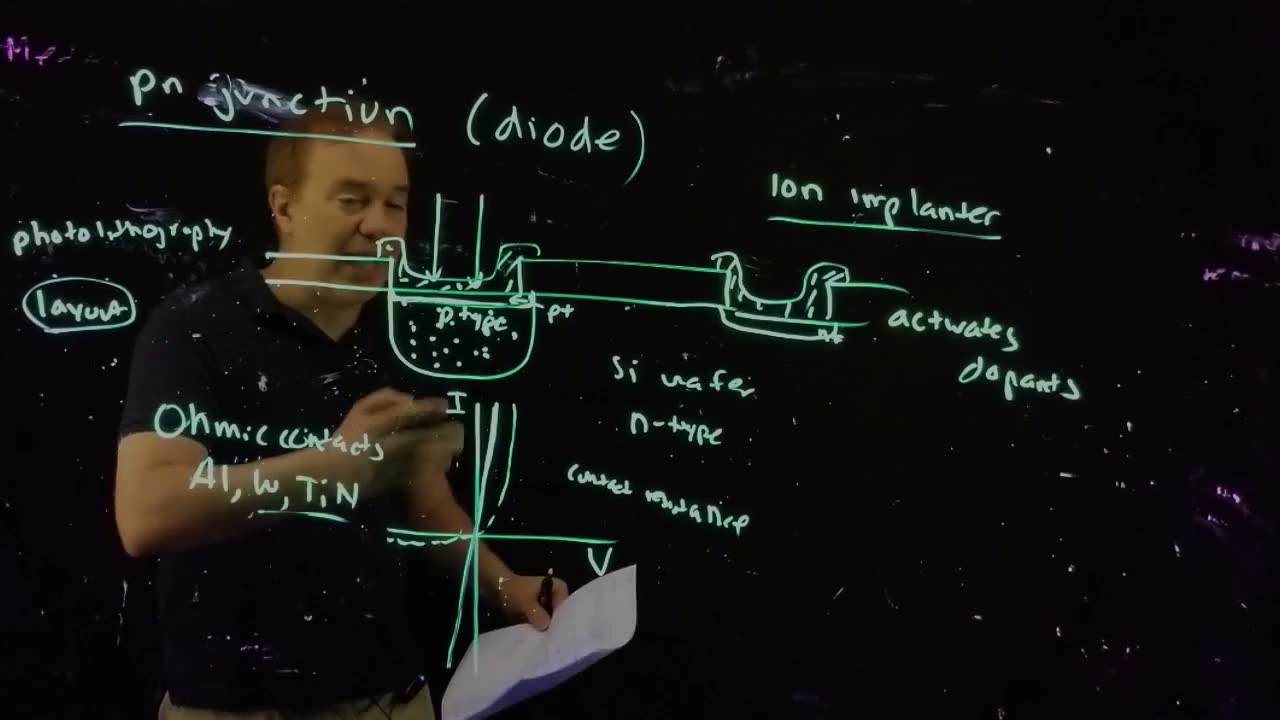
The lecture sketches the process “in very crude terms” (38:00); taped Lecture 9 returns to fabrication. Follow the steps on an n-type wafer (39:08):
A pn junction, step by step (38:30–47:10)
- Oxidize (38:42). Put the wafer in a furnace with oxygen or water. A layer of silicon dioxide, SiO₂ (glass), grows on the surface.
- Coat with photoresist (39:46). Spin a light-sensitive photoresist over the wafer.
- Expose (39:46). A stepper or mask aligner projects the image on a mask onto the resist with ultraviolet light. Depending on whether the resist is positive or negative, the exposed parts become easier or harder to remove.
- Develop (40:17). A chemical developer removes the resist over the chosen region, opening a window. This pattern transfer from mask to resist is photolithography. Layout, which you will do in this course, is designing the shapes on these masks (40:56).
- Etch the oxide (41:33). Dip the wafer in hydrofluoric acid (HF). HF etches glass but not silicon, so it opens the window through the oxide.
- Strip the resist (41:48) in acetone or another solvent. Now the wafer carries a patterned oxide.
- Implant (42:18). An ion implanter ionizes boron and accelerates it to kiloelectron-volt energies, blasting the ions into the silicon through the window. The oxide blocks them elsewhere. The dose (how many ions) sets how much boron goes in; the energy sets how deep it goes (43:12).
- Anneal (43:27). The implant knocks silicon atoms out of place. Heating the wafer repairs the damage and activates the dopants: the boron atoms take lattice sites, accept electrons and release holes (43:55). The implanted region is now p-type inside the n-type wafer.
- Contact regions (44:34). A second window over the substrate (which the lecturer admits he should have opened in step 4) and two more implants make a heavily doped p⁺ region at the surface of the p region and a small n⁺ region in the n wafer. The plus means heavily doped.
- Metal (45:11). Metal on each contact region connects the device to the outside.
Ohmic contacts
Why the and regions? To make good ohmic contacts (45:00). An ohmic contact between metal and silicon has a current–voltage curve that is a straight line through the origin, as steep as possible: a small contact resistance (45:55).
The alternative is a metal–semiconductor contact whose I–V curve looks like a diode’s. That is a Schottky barrier diode (46:28); sometimes it is wanted as a diode, but not here. Two things make the contact ohmic (46:37):
- heavy doping of the silicon under the metal (the and regions);
- a careful choice of metal, with an appropriate anneal. For silicon the lecture lists aluminium, tungsten and titanium nitride board. (It calls them all refractory metals. Strictly, tungsten is a refractory metal and TiN a refractory compound, but aluminium, which melts at 660 °C, is not added.)
Now the current between the two contacts is set by the pn junction between the p region and the n wafer, plus a little access resistance (47:10). The rest of the lecture draws a line through that junction and studies it in one dimension (47:45).
Check yourself In the implant step, what do the dose and the energy each control?
The dose (the number of ions per area) controls how much dopant goes in; the energy controls how deep the ions go. After the anneal activates them, the dose and depth together set the doping profile.
Check yourself Why are the regions under the metal contacts doped p⁺ and n⁺?
Heavy doping under the metal makes the contact ohmic: a straight, steep I–V line with low resistance, instead of a rectifying Schottky barrier.
9. The pn junction in equilibrium
The idea. When p and n silicon meet, carriers diffuse across, leave behind fixed ion charge, and build a field that stops further diffusion. The Fermi level becomes flat and the bands bend.
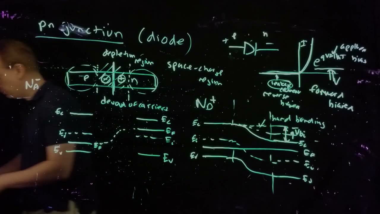
The simple picture (48:58). Put p-type material directly against n-type material. The plane where the doping changes from p to n is the metallurgical junction (49:13).
How the junction reaches equilibrium (49:13–55:19)
- Before contact. Draw each side’s band diagram separately. The p side’s Fermi level is low in the gap; the n side’s is high (49:45).
- Equilibrium needs one Fermi level. In thermal equilibrium the Fermi level must be the same everywhere; different Fermi levels would mean the system isn’t in equilibrium (49:57).
- Diffusion. The p side is full of holes and the n side has almost none, so holes make “a beeline” for the n side. Electrons likewise rush to the p side (50:34). There they recombine with the majority carriers.
- A depletion region opens (50:40). Near the junction the mobile carriers are gone: the region is depleted of mobile carriers.
- Fixed charge is left behind (51:46). Each donor that lost its electron is a positive ion (); each acceptor that gained one is a negative ion (). The n side of the region is positive, the p side negative. Because it holds net charge, it is also called the space-charge region.
- A field appears (52:50). The space charge creates an electric field that pushes back against the diffusion. When the two balance, the net current is zero and the junction is in equilibrium (53:19).
- The bands bend (53:53). With one flat , the bands on the two sides must shift relative to each other. , and all bend through the space-charge region: band bending. Outside it the bands are flat.
Bent bands mean a field (54:53). Wherever the bands are not flat, there is an electric field; where they are flat, there isn’t. So the field lives only in the depletion region, together with the charge.
The barrier (55:38). The band bending is an energy barrier inside the diode. Its height is , where is the built-in voltage board. The barrier holds back the diffusion; that’s why no net current flows in equilibrium.
The electrostatics of the junction, the shapes of the charge, field and potential, and the formulas for and the depletion width are the subject of Lecture 3: see Chapter 3.
Common mistakes.
- Confusing the metallurgical junction with a metal contact. added The metallurgical junction is where the doping changes type; it has nothing to do with metal.
- Thinking the built-in voltage could drive a current, like a battery. added It is an equilibrium barrier: the field it represents exactly balances diffusion, so no current flows, and connecting a wire across the diode gives nothing.
- Expecting the depletion region to be neutral. It is the one place with net charge; the neutral regions are outside it.
Check yourself Which side of the depletion region is positively charged, and why?
The n side. Its donors have given up their electrons, which diffused away, leaving fixed positive donor ions (). The p side holds negative acceptor ions ().
10. Forward and reverse bias: why it’s a diode
The idea. A voltage that lowers the barrier lets carriers flood over it, and the current rises exponentially. A voltage that raises the barrier stops them, leaving only a tiny leakage.
Forward bias (56:31). Make the p side positive relative to the n side by an applied voltage . The junction leaves equilibrium, so a single no longer applies (56:31), but the key effect is simple: the barrier drops by .
- Electrons from the n side now cross to the p side, where they are minority carriers, and holes cross from p to n. This is minority-carrier injection (57:05), and it is a large current.
- The carriers have Maxwell–Boltzmann statistics, so the number with enough energy to clear the barrier grows exponentially as the barrier falls (57:45):
A rule worth remembering (57:45): whenever a current–voltage characteristic has the form , carriers are crossing a barrier. This exponential is fundamental to most semiconductor devices; it comes back as the MOSFET’s subthreshold current (58:12, Chapter 4).
Reverse bias (58:42). Make the p side negative relative to the n side. The barrier rises, and very little current flows (59:04). What remains is leakage current: “a current that ideally you would like to be zero but isn’t” (59:23). In typical MOS structures, junction leakage is in the femtoamps (). Some current still flows, for example from electron–hole pairs generated thermally in the depletion region (59:51).
That asymmetry, large exponential current one way and almost none the other, is what makes the pn junction a diode.
The full diode law. added The Fall 2026 class wrote the ideal-diode equation . For forward bias of more than about the is negligible, which gives the board’s . In reverse bias the exponential vanishes and , a small leakage.
Worked example. added How much more current flows for each extra 0.1 V of forward bias, and how much bias raises the current a millionfold?
- A factor of 10 in current needs , so : about 60 mV per decade of current.
- An extra 0.1 V multiplies the current by .
- A factor of is six decades: .
Common mistakes.
- Getting the polarity backwards. Forward bias puts the p side positive; the diode symbol’s arrow points from p to n, the direction of forward current.
- Expecting the reverse current to be exactly zero. It is tiny (leakage), not zero.
Check yourself A diode carries 1 µA at some forward bias. Roughly what current flows at 120 mV more forward bias?
120 mV is about two decades at 60 mV per decade, so roughly : about 100 µA. (Exactly, .)
Formulas to remember
| Formula | Meaning |
|---|---|
| , at 300 K, | silicon at room temperature |
| intrinsic conductivity rises exponentially with | |
| intrinsic silicon | |
| mass-action law, in equilibrium, doped or not | |
| , | n-type: electrons majority, holes minority |
| , | p-type: holes majority, electrons minority |
| , | Fermi–Dirac occupancy |
| , | carriers from (not degenerate) |
| , | Fermi level from doping; 60 meV per decade |
| forward diode current; 60 mV per decade; means a barrier |
The lecture’s boards