16. Adders: the full adder, the carry chain and lookahead
Lecture 15 opens the part of the course about datapaths: the blocks that do the same operation on every bit of a word. The first and most important is the adder. The lecture starts from a single bit, the full adder, whose two outputs turn out to be two famous logic functions. Chaining full adders gives the ripple-carry adder, and its delay is set by the carry rippling from the bottom bit to the top. The lecture then builds the full adder from transistors and uses two of its properties to make the carry chain fast. One is self-duality, which makes every pull-up network a mirror of its pull-down; the other is the late arrival of the carry. After a short look at how a datapath is laid out, it turns to parallel adders, which spend hardware to compute the carries without waiting for the ripple. Each one starts from the same rewriting of the carry into generate and propagate: carry bypass, carry select and, the way adders are really built, carry lookahead, ending at a radix-4 lookahead tree. The next lecture continues with radix-2 trees (Chapter 17).
After this chapter you can:
- write a full adder’s two outputs as the majority and the odd parity of its inputs, and check them against the truth table;
- find the critical path of a ripple-carry adder and count its stages;
- turn an adder into a subtractor;
- say what a self-dual function is and why it makes a gate’s pull-up and pull-down identical;
- draw the mirror adder’s carry and sum stages, place correctly, and compute their logical efforts;
- remove the carry chain’s inverters by alternating polarity, and compute what it saves and when;
- lay out a datapath as a bit stack with a uniform bit pitch;
- define generate and propagate, and say why the sum needs ;
- trace the critical paths of carry-bypass, carry-select and lookahead adders and compare them;
- unroll the carry recursion into group generate and propagate, combine two groups, and build a radix-4 lookahead tree.
Boxes and equations marked board were written in the lecture. Parts marked added are explanations, arguments or examples this guide adds; every number in them is recomputed in the page’s test.
Before you start. Three things from earlier chapters run through this one. Complementary static CMOS (Chapter 7, §4): a gate’s NFET pull-down network conducts when the output should be 0, and its PFET pull-up is the dual network, series and parallel exchanged. The course’s delay model (Chapter 8, §1): a stage’s delay is its gain in units of , where is its logical effort and its load over its input capacitance; drain capacitance is ignored. Binary numbers (Chapter 15, §11): bit 0 is the least significant, and two’s complement negates by inverting every bit and adding 1. One note on the recording: Lecture 15 was taped in two takes. At 21:44 the board is suddenly clean, because the second half was re-recorded; nothing is lost between them.
Symbols
| Symbol | Meaning | Unit | First appears |
|---|---|---|---|
| , ; , | the two operand bits; bit of each operand (bit 0 the least significant, drawn at the right) | — | §1, §2 |
| , | a full adder’s carry in and carry out | — | §1 |
| , | a full adder’s sum bit; bit of the sum | — | §1, §2 |
| , | the complement of (the board’s overbar) | — | §1 |
| exclusive OR (XOR) | — | §1 | |
| the carry into bit : , and bit ‘s carry out is | — | §2, §12 | |
| the number of bits in the adder | — | §2 | |
| , | the delay of one carry stage and of one sum stage added | §2 | |
| SUB | the subtract control bit added | — | §3 |
| (no bit index) | logical effort, Chapter 7’s: an input’s capacitance over that of an inverter of the same drive. Written with a word subscript where it could be confused with a generate: , | — | §5 |
| electrical effort: a stage’s load over its input capacitance | — | §5 | |
| the fan-out-of-one (FO1) inverter delay, the unit of the gains | ps | §5 | |
| units | gate width in multiples of the reference inverter’s NFET (inverter: NFET 1, PFET 2, input 3) | — | §5 |
| the size of an inverter in the carry chain, in multiples of the reference inverter added | — | §7 | |
| the input capacitance the next bit’s sum stage puts on the carry wire added | units | §7 | |
| , | generate and propagate of bit (always with a bit index, or as "" in §9) | — | §9 |
| the number of bits in a group (bypass) or bin (select) added | — | §10 | |
| a group’s propagate: the AND of its bits’ | — | §10 | |
| , | the delay of a 2:1 multiplexer and of a PG cell added | §10 | |
| , ; , | group generate and group propagate (the board’s braces); the subscript names the bits, high index first added | — | §12 |
| LA | a lookahead unit (radix 4: it takes four bits or four groups) | — | §13 |
| the delay through one lookahead unit added | §13 | ||
| the number of levels in a lookahead tree added | — | §13 |
1. The full adder: majority and odd parity
You need
Binary addition by hand added. Add column by column, starting at the least significant bit (the right). In each column add the two bits and the carry that came in from the right. A column that adds to 0 or 1 writes it and carries 0; one that adds to 2 (binary 10) writes 0 and carries 1; one that adds to 3 (binary 11) writes 1 and carries 1.
XOR added. when exactly one of , is 1. It is associative, so needs no brackets: it is 1 when an odd number of , , are 1.
The question. Every adder, however fast, is built from one-bit pieces. What does the piece for one column of a hand addition compute, and what logic functions are its outputs?
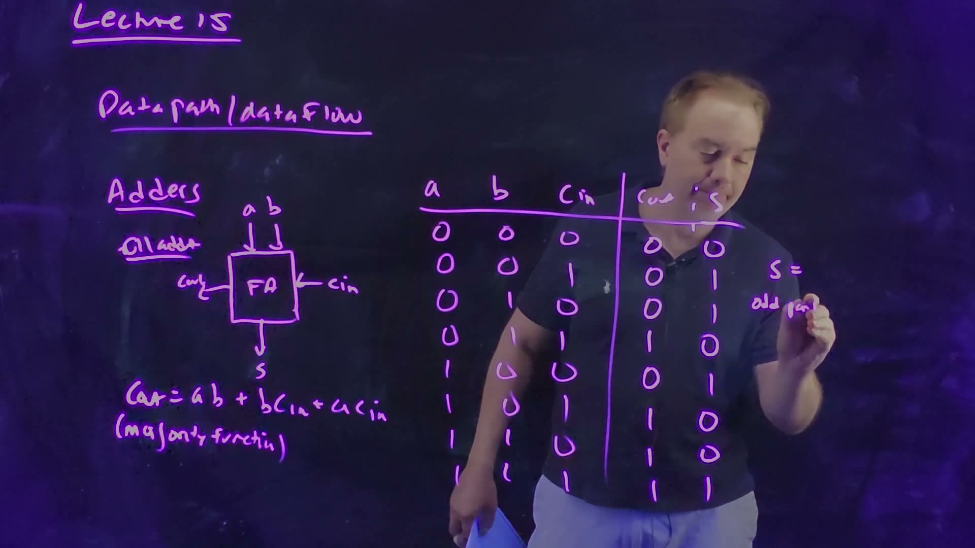
The block is the full adder (FA) board (00:51). It takes three bits, the two operand bits and and the carry coming from the column to its right, and gives two: the sum bit and the carry into the column to its left. The board draws it the way hand addition runs: and from above, from the right, out to the left and out below. Keep that orientation: in every chain in this chapter, bit 0 is at the right and the carry flows right to left.
The full adder, redrawn from the board (Lecture15 @ 03:52). Left: the block, with the carry entering from the right and leaving to the left, as in hand addition. Right: its truth table. Read each row as a count: and are the number of ones among , , , written in binary.
The board (Lecture15 @ 03:52)
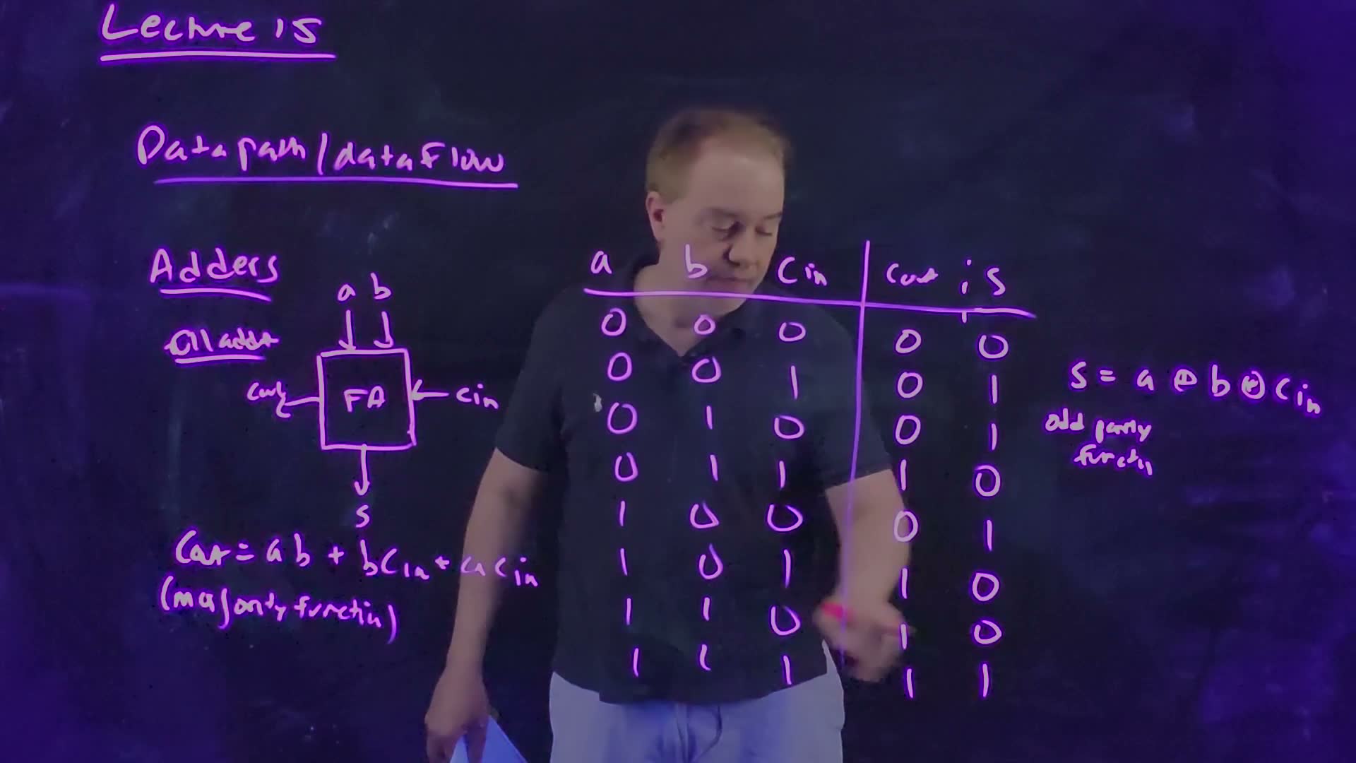
Fair copy of the board above (Lecture15 @ 03:52), mark for mark in its own layout. All black: one pen wrote the whole board. The bottom of the table’s vertical rule, behind the lecturer’s hand here, is copied from 03:23. The table’s rows are levelled; on the board they drift down to the right.
From the truth table to two functions (board, 01:16–03:56)
- The table. Eight rows, one for each combination of , , (01:16–02:11). Read one in words: row 011 is , binary 10, so and .
- The carry is the majority. is 1 in rows 011, 101, 110 and 111: exactly the rows where at least two of the three inputs are 1. As a sum of products, one product for each pair of inputs that are both 1 (02:12–03:06) board: . The board names it the majority function: the output agrees with the majority of the inputs.
- The sum is the odd parity. is 1 in rows 001, 010, 100 and 111: one or three ones, an odd number. That is (03:06–03:56) board, the odd parity function.
- Why the block adds added. In every row, : the two outputs are the count of ones written in binary, the twos digit and the ones digit. That is what a column of hand addition needs.
The last column below is the count, which the two outputs encode:
| 000 | 0 | 0 | 0 |
| 001 | 0 | 1 | 1 |
| 010 | 0 | 1 | 1 |
| 011 | 1 | 0 | 2 |
| 100 | 0 | 1 | 1 |
| 101 | 1 | 0 | 2 |
| 110 | 1 | 0 | 2 |
| 111 | 1 | 1 | 3 |
Memorize or derive. Memorize both: they are the most-used formulas of the chapter, and their names (majority, odd parity) carry them. is the one-line derivation if you forget: count the ones and write the count in binary.
A worked example (the board’s rows). Row 011: , , , so ; , so ; and . Row 111: all three products are 1, so ; ; and .
Traps.
- Reading as an OR. in Boolean algebra is the OR, which is 1 on row 011; the sum bit there is 0. The sum is the parity, not the OR.
- Dropping a product term. misses row 101 (, ), where the carry is 1. Each of the three pairs needs its term.
Check yourself Which rows of the full adder's truth table have cout = 1 and s = 0?
Rows 011, 101 and 110: exactly two of the three inputs are 1, so the count is 2, binary 10.
Check yourself Show from the table that cout does not change when you exchange a and cin. What property of the formula guarantees it, and does s have it too?
Exchanging and maps row 001 to 100 and 011 to 110 (rows 000, 010, 101 and 111 map to themselves); in each pair is the same (0 and 0; 1 and 1). The formula is symmetric in its three inputs: exchanging any two permutes its terms. So is , so has it too. A full adder does not care which input is the carry, which §5 and §6 exploit.
2. The ripple-carry adder and its critical path
You need
The full adder (§1). Three bits in, two out: (1 when at least two inputs are 1) and (1 when an odd number are). The carry enters from the right and leaves to the left.
Synchronous timing (Chapter 13). Logic between flip-flops must settle within one clock period, for every input: the period is set by the slowest path through the logic.
The question. Chain full adders and you have an -bit adder. How long does it take, and which path through it sets that time?
Ripple carry (board, 04:36–08:30)
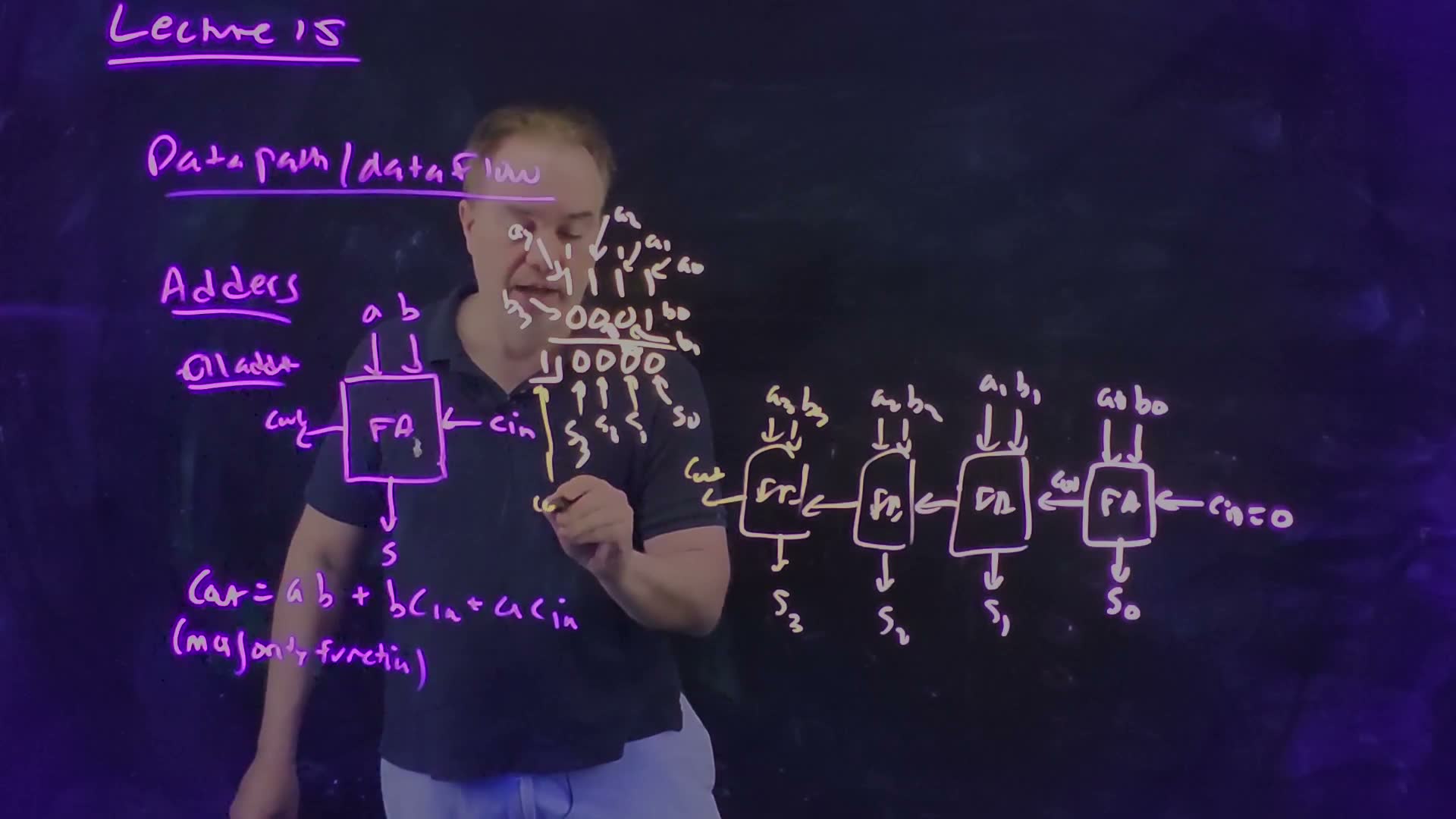
- Hand addition. Add 1111 and 0001 (04:41). The right column is : write 0, carry 1. The next is : write 0, carry 1. And so on: “one and one is zero, carry the one”, four times. The result is 0000 with a carry out of 1, which is .
- The circuit. One full adder per column, right to left (05:09–06:28) board. Bit 0’s carry-in is ; bit takes and from above and gives below; each carry-out goes into the next bit’s carry-in, and the last carry-out is the adder’s . The carry ripples from bit to bit, so this is the ripple-carry adder board.
- The delay depends on the operands. In 1111 + 0000 no column makes a carry: every bit’s sum is ready as soon as its own , arrive (07:10). In 1111 + 0001 the carry made at bit 0 must pass through every bit before the top sum is right.
- The clock must wait for the worst. “In a synchronous design, I have to wait for the longest answer” (07:38). So we time the adder by its worst-case path, the critical path board: a carry made at bit 0 that ripples through every carry circuit to the top.
- What to optimize. On that path the carry circuit appears once per bit, and a sum circuit only once, at the end. For an 8-bit adder the critical path includes “eight copies of the carry chain” (15:53), the lecturer says, and the sum appears on it once. So the carry logic is what matters; a slow sum circuit costs only once.
The board’s two additions added (values from Lecture15 @ 09:32). Left: 1111 + 0001 makes a carry in every column; the result is 0000 with a carry out of 1. Right: 1111 + 0000 makes no carry at all. The same adder finishes sooner for the right-hand pair, but the clock cannot know which pair is coming.
A 4-bit ripple-carry adder, redrawn from the board (Lecture15 @ 09:32). Each carry-out feeds the next bit’s carry-in, from bit 0 at the right to bit 3 at the left. The thick line is the critical path: a carry made at bit 0, rippling through every carry to the top sum .
The board (Lecture15 @ 09:32)
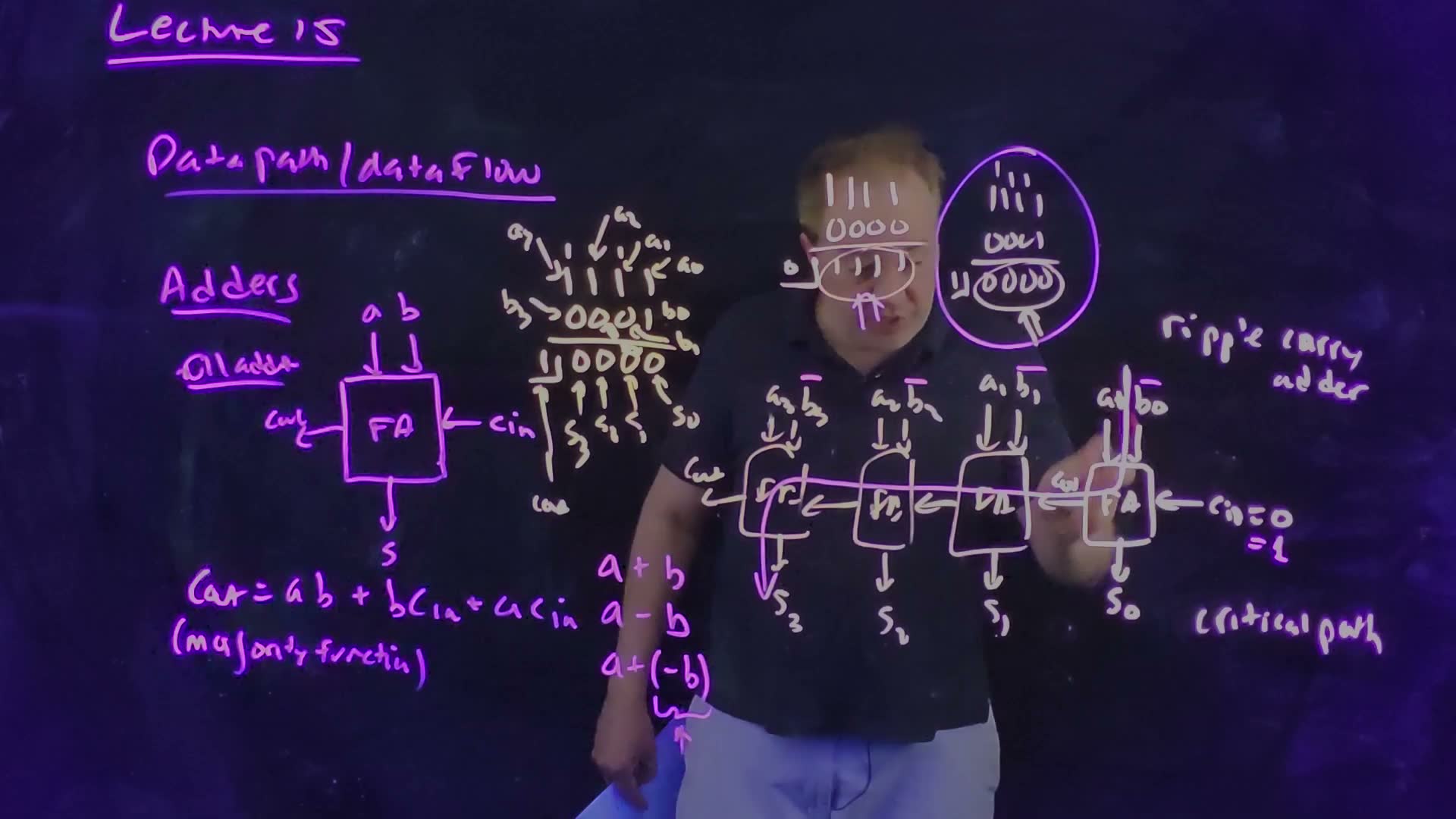
Fair copy of the board above (Lecture15 @ 09:32), mark for mark in its own layout. Orange is the pale pen, which drew the ripple-carry adder and its examples: the column sum, the two small sums and the chain with its labels. Black is the violet pen: the full-adder notes from 03:52 and, over the orange, the marks added afterwards: the ring round the worst case, the critical path into , and the subtraction ( and for ). The left edge of bit 0’s box, the carry into bit 1 and its label, behind the lecturer’s hand here, are copied from 08:47. The table and the parity function of 03:52 are erased by now.
Counting the critical path
Let be the delay of one carry circuit (from its carry-in to its carry-out) and that of one sum circuit added. Follow the carry made at bit 0.
- The carry into bit , , comes out of carry circuits (bits 0 to ).
- If the sum circuit needs only , and the carry into its bit, as does, the top sum follows one sum delay later: .
- The carry-out needs one more carry circuit: .
- The lecture’s circuit (§5) computes its sum from its own bit’s carry-out, so the top bit’s carry circuit also lies on the path to : . That is the lecturer’s count for 8 bits, eight carry stages and one sum, and the eight-stage drawing below.
The critical path of an 8-bit ripple-carry adder, redrawn from the board (Lecture15 @ 18:06): eight carry stages and one sum stage. Every bit adds a carry stage to the path; the sum stage is paid once.
From §9 on, every adder forms its sums as from the carry into its bit, so the comparisons there use the first count.
Memorize or derive. Derive: trace the carry from bit 0 and count the circuits it passes. The one thing to remember is that the delay is linear in : double the width, double the time.
A worked example. First the board’s two additions: 1111 + 0001 gives carries , sum 0000 and (16); 1111 + 0000 gives no carries and sum 1111 (15). Now some delays added: take, for example, (§7 finds 4 for the lecture’s carry stage with its inverter removed and a light sum stage; with an inverter it is about 5). An 8-bit adder’s top sum arrives after and its after ; with the lecture’s circuit, whose sum waits for its own carry stage, the top sum takes . A 32-bit adder’s top sum takes : four times the width, four times the delay.
Traps.
- Timing the adder by a typical input. Most additions finish early, but the clock has to cover 1111 + 0001.
- Optimizing the sum first. The sum circuit is on the path once; the carry circuit times.
Check yourself Which 4-bit operand pairs (with cin = 0) make a carry ripple from bit 0 all the way to cout?
Bit 0 must generate a carry, , and each of bits 1 to 3 must pass it on, which needs exactly one of , to be 1. For example 1111 + 0001, or 0101 + 1011.
Check yourself With the example delays, an 8-bit ripple adder's carry stage gets faster, from 5 to 4 τinv. How much sooner does cout arrive? If instead the sum stage got 1 τinv faster, how much sooner would cout arrive?
Step 1: passes eight carry stages, so it goes from to : sooner. Step 2: no sum stage lies on the path to , so a faster sum stage changes it by nothing. (The top sum would gain ; the carry stage’s speed-up gains it seven, one per carry stage before it.)
3. Subtraction with the same adder
You need
Two’s complement (Chapter 15, §11). An -bit word with its top bit as the sign. To negate a number, invert every bit and add 1: . A carry out of the top bit is dropped.
XOR as a controlled inverter added. and : an XOR passes when its other input is 0 and inverts it when it is 1.
The ripple-carry adder (§2): full adders chained right to left, bit 0’s carry-in free.
The question. Can the same adder subtract, without a second circuit?
a − b on an adder (board, 08:30–09:30)
- Rewrite the subtraction. board.
- Negate in two’s complement. Invert every bit of (the board’s overbars on ) and add 1 board.
- Use the free carry-in for the “+1”. Bit 0’s carry-in is otherwise 0; set it to 1 (the board’s “ / ”). Nothing else in the adder changes.
- One control bit (09:30, spoken). A bit SUB added does both: XOR it into every , and wire it to . SUB = 0 adds; SUB = 1 subtracts.
An adder–subtractor added, as described in the lecture (09:30). One control bit SUB feeds an XOR on every and bit 0’s carry-in. SUB = 0: the XORs pass and , so the circuit adds. SUB = 1: the XORs invert and , so it computes .
Memorize or derive. Derive: negation in two’s complement is invert-and-add-one, and the adder’s carry-in supplies the one.
A worked example added (4 bits). : and , so , with a carry out of 1, dropped. : , which in two’s complement is , with a carry out of 0.
Trap. Inverting but leaving computes : comes out as 0001.
Check yourself What does the 4-bit subtractor output for 0 − 1, and how do you read the result?
Step 1: , so the adder computes . Step 2: read it in two’s complement: the top bit is 1, so it is negative; inverting and adding 1 gives , so . Correct.
Check yourself With SUB = 1, what does the 4-bit circuit give for 4 − 4, and why is its carry-out 1?
Step 1: , so the adder computes : sum 0000, carry-out 1. Step 2: inverting and adding 1 adds , so the adder computes , which reaches 16, and carries out, exactly when as unsigned numbers. Here , so the carry-out is 1. (In 5 − 3 it was 1 too; in 3 − 5 it was 0.)
4. Self-duality: why the pull-up equals the pull-down
You need
Complementary static CMOS (Chapter 7, §4). The NFET pull-down network conducts on the rows where the output is 0, so the gate computes the complement of the pull-down’s condition. The PFET pull-up is the dual network: the same inputs, with every series connection made parallel and every parallel one series. A PFET conducts on a 0. Exactly one network conducts for every input, so the gate is static.
The two outputs (§1): , the majority, and , the odd parity.
The question. To build the full adder in static CMOS we need a pull-down and a pull-up for each output. What special property do these two functions have, and what does it buy in the circuit?
Self-duality (board, 10:04–12:16)
- The definition (10:51) board. Complement all three inputs, and the output complements: and . A function with this property is self-dual board. Check one row: , and .
- Why it holds added. Complementing all three inputs turns a count of ones into . “At least two of three” becomes “at most one”, the complement of the majority; an odd count becomes an even one, the complement of the parity.
- What it buys (11:35–12:06). A pull-up of PFETs conducts when its inputs are low; so a pull-up network built with the same series–parallel structure as the pull-down, on the same inputs, conducts exactly when the pull-down would conduct on the complemented inputs. For the gate to work, the pull-up must conduct when the output is 1, which is when the pull-down is off. For a self-dual function those two conditions coincide, so the pull-up can have the same structure as the pull-down. “If the logic function in question is self dual, then the pull-up and pull-down networks will be exactly the same. And that’s going to make the layout very convenient.”
- The majority’s networks added. Its pull-down conducts for : in series with ( parallel ), and beside that branch in series with . Chapter 7’s rule would build the pull-up as the dual: swap series and parallel everywhere, giving ( parallel –) in series with ( parallel ). That works, but self-duality offers a second pull-up: the pull-down’s own structure in PFETs, which by step 3 conducts exactly when the output should be 1. The two pull-ups conduct for the same inputs; only the second is a mirror image of the pull-down, and that is the one the lecture uses. The pull-down and its mirror are drawn below.
The majority’s pull-down and the mirror pull-up added. Left: the pull-down, conducting for . Right: the same structure in PFETs, conducting for , the majority of the complemented inputs, which by self-duality is 1 exactly when . The two networks are the same up to the order of devices in a branch, which is why the lecture’s circuit (§5) has a pull-up that mirrors its pull-down.
The board (Lecture15 @ 11:45)
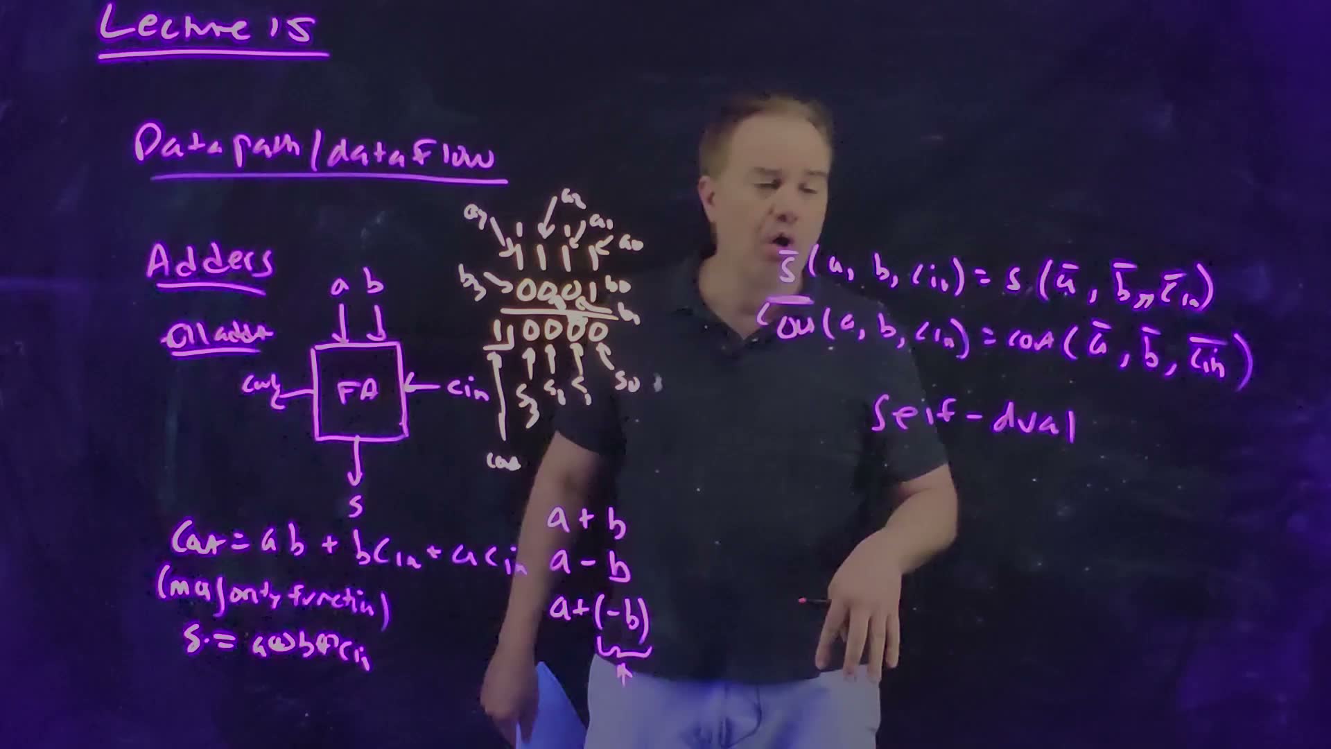
Fair copy of the board above (Lecture15 @ 11:45), mark for mark in its own layout. Orange is the pale pen’s column sum, the one part of 09:32’s ripple-carry layer still on the board; everything else is the violet pen, in black. The two small sums, the ripple chain with its critical path, “ripple carry adder” and “critical path” are erased by now. The two equations are levelled; on the board they drift down to the right.
The sum written with the carry
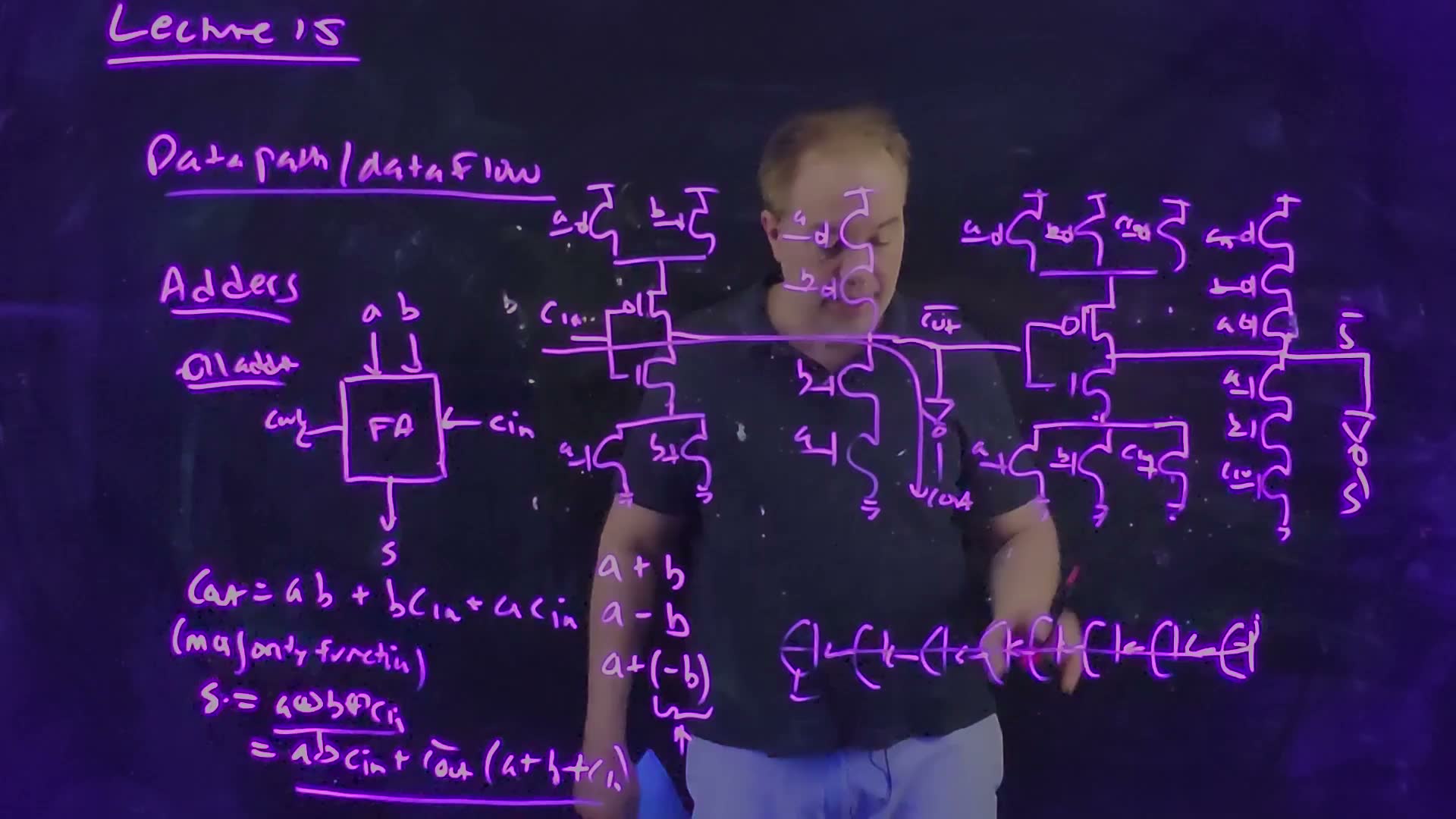
The board also rewrites the sum in a form the circuit will use (12:41, written at 18:06) board:
Why it is right, case by case:
- No input or one input is 1. Then , so , and the second term is : 1 when exactly one input is 1, 0 when none is. The product is 0. So is 1 for one input, 0 for none. Correct.
- Exactly two are 1. kills the second term, and . So . Correct.
- All three are 1. . So . Correct.
The point: a three-input XOR in static CMOS is large, but this form needs only AND and OR of the inputs and of , which the carry gate already makes. The table checks both properties on every row:
| 000 | 0 | 1 | 0 | 1 | 0 |
| 001 | 1 | 0 | 0 | 1 | 1 |
| 010 | 1 | 0 | 0 | 1 | 1 |
| 011 | 0 | 1 | 1 | 0 | 0 |
| 100 | 1 | 0 | 0 | 1 | 1 |
| 101 | 0 | 1 | 1 | 0 | 0 |
| 110 | 0 | 1 | 1 | 0 | 0 |
| 111 | 1 | 0 | 1 | 0 | 1 |
Memorize or derive. Memorize the definition of self-dual, and that both full-adder outputs have it. Derive the sum identity from the three cases above when you need it: it is the form that FN12-10b’s domino full adder and MT24-5a’s dynamic one use.
A worked example (the identity on two rows). Row 110: , so , and : , as (binary 10) says. Row 100: and , so .
Traps.
- “The two outputs are duals of each other.” The lecturer says it loosely (10:38), but the property is that each output is its own dual.
- Every gate’s pull-up mirrors its pull-down. No: a NAND’s pull-down is series and its pull-up parallel. Only a self-dual function can have identical networks.
- The mirror is the dual. It is not: the dual of the majority’s pull-down is ( parallel –) in series with ( parallel ), a different arrangement of the same five devices. The two conduct for the same inputs, which is why either serves; the mirror is chosen because it matches the pull-down in the layout.
Check yourself Is a two-input XOR self-dual?
No. Complementing both inputs leaves an XOR unchanged, , but self-duality needs it to complement. An XOR of an odd number of inputs is self-dual; an even number is not.
Check yourself Is the complement of the majority, c̄out, also self-dual? What does the answer say about the gate that produces c̄out?
Step 1: complement both sides of : , which is the definition of self-duality for . Step 2: the gate that computes (a static CMOS gate always computes a complement) can therefore have identical pull-up and pull-down. That is the carry stage of §5.
5. The mirror adder at transistor level
You need
Sizing stacks and logical effort (Chapter 7, §8). The reference inverter has an NFET of 1 unit and a PFET of 2 units (the PFET is half as strong per width), so its input is 3 units. To give a gate the same drive, every conducting path must be as strong as one inverter device, so a device in a series stack of is times as wide. An input’s logical effort is its gate width over the inverter’s 3 units: a two-input NAND (NFETs 2, PFETs 2) has .
Self-duality (§4). Both full-adder outputs are self-dual, so each gate can have a pull-up with the same structure as its pull-down. The majority’s pull-down is over ( parallel ), beside – in series.
The sum identity (§4): .
The question. What does the lecture’s full adder look like in transistors, and what does it cost to drive its inputs?
The lecture draws a static CMOS full adder device by device (12:16–15:17) but gives it no name. This guide calls it the mirror adder added, because every pull-up in it is the mirror image of its pull-down, and that is the name it goes by in textbooks.
The two stages (board, 13:20–15:11)
- The carry stage. The pull-down: an NFET over NFETs and in parallel, and beside that branch NFETs and in series (13:20–14:10) board. It conducts when , the majority, so the gate’s output is . The pull-up is the same structure in PFETs, which self-duality allows. An inverter after it gives .
- The sum stage. The pull-down: an NFET over NFETs , , in parallel, and beside it NFETs , , in series (14:10–15:11) board. It conducts when , which by §4’s identity is , so the output is . Again the pull-up is the same structure in PFETs, and an inverter gives .
- Count the devices added. Carry stage: 5 NFETs and 5 PFETs, 10. Sum stage: 7 and 7, 14. Two inverters, 4. In all, 28 transistors.
The mirror adder’s carry stage, redrawn from the board (Lecture15 @ 21:39). The pull-down conducts for , so the output is ; the pull-up has the same structure in PFETs. The two devices sit next to the output node (§6 explains why), and an inverter restores .
The mirror adder’s sum stage, redrawn from the board (Lecture15 @ 21:39). Its pull-down conducts for , which is (§4), so the output is ; an inverter gives . The input comes from the carry stage.
The board (Lecture15 @ 18:06)
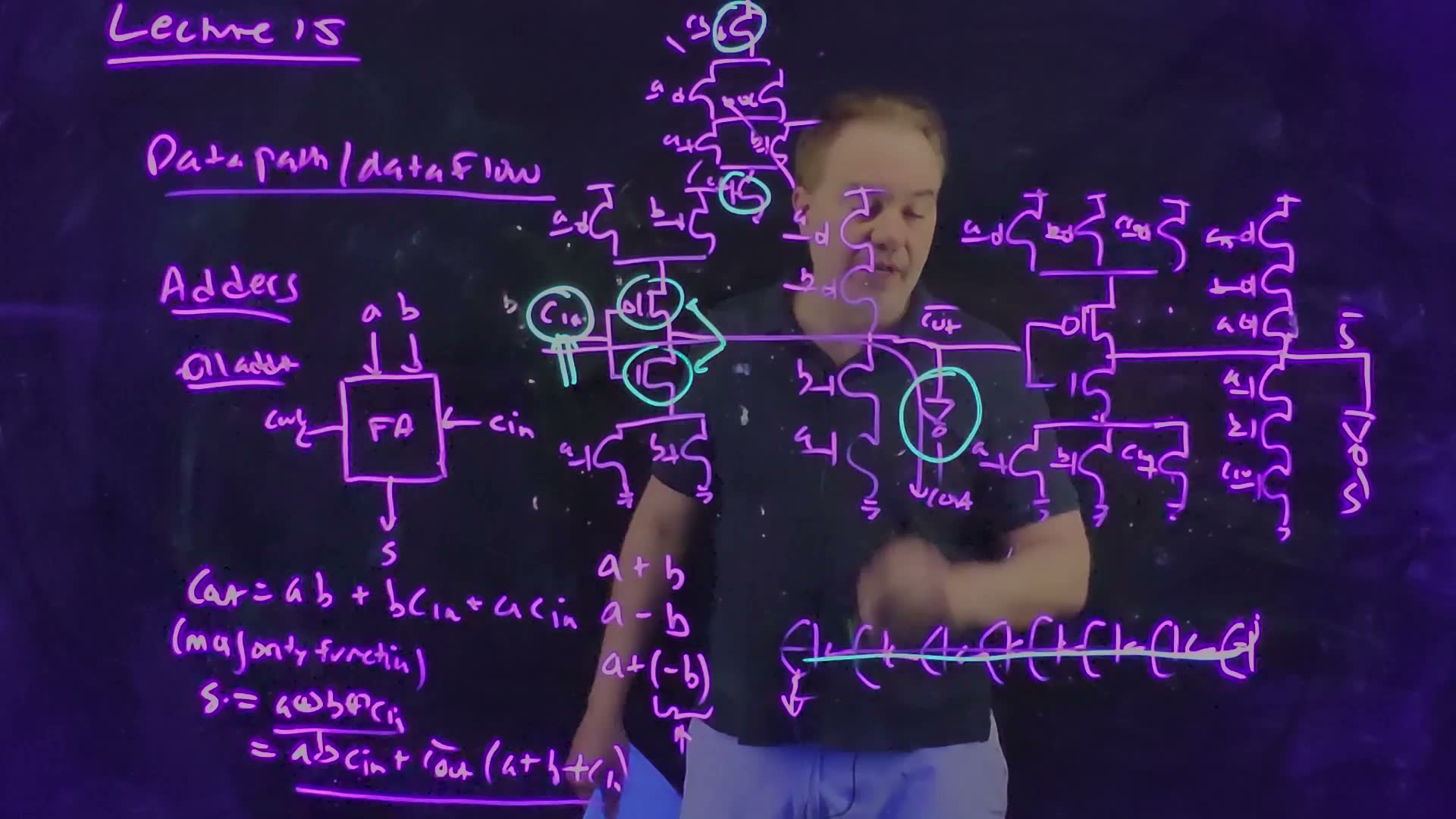
Fair copy of the board above (Lecture15 @ 18:06), mark for mark in its own layout. Black is the violet pen: the notes from 03:52–11:45 with the sum identity added, the carry stage (output , then an inverter to ), the sum stage (output , then an inverter to ), the alternative carry stack at the top, struck through, and the eight-stage carry chain. Teal is the cyan pen, added over the finished circuit: the rings on the input and on the two devices next to the output, the rings on the top stack’s devices next to the rails, the ring on the carry inverter, and the line along the chain’s carries. The – column of the carry stage lies over the lecturer’s face, which washes out its labels; they match 21:39, where the column is unchanged. The lone left of is what is left of 09:32’s column sum. The devices are drawn with the course’s symbols; the board draws squiggle channels.
Sizing the stages and their logical efforts
Now size each stage, by Chapter 7’s stack rule, to drive like the reference inverter added.
The carry stage sized for the reference inverter’s drive added. Every path through each network passes two devices, so every NFET is 2 and every PFET 4. The wire drives one NFET and one PFET, 6 units; the wire (and likewise ) drives two of each, 12 units.
Widths and logical efforts (Chapter 7's sizing)
- Carry stage widths. Every path from the output to ground passes two NFETs ( then or ; or then ), so every NFET is . Every path in the pull-up passes two PFETs, so every PFET is .
- Carry stage, input. It drives one NFET (2) and one PFET (4): 6 units. Logical effort .
- Carry stage, input (and ). It drives two NFETs and two PFETs, one in each branch: units, so .
- Sum stage widths. The series branch –– is three high, so those NFETs are 3 and PFETs 6. In the other branch every path passes two devices ( and one of the parallel three), so those are 2 and 4.
- Sum stage inputs. drives one 2 and one 4: 6 units, . The input drives a 3 and a 2 (NFETs) and a 6 and a 4 (PFETs): 15 units, . So do and .
Memorize or derive. Derive: size by the stack rule, add up the input’s gate widths, divide by 3. It takes a minute and needs nothing memorized.
The worked example’s lesson. The input costs half as much to drive as or . That is just right, because is the input on the critical path (§2): each carry stage drives the next one’s , so its light load makes the chain fast. The sum stage is heavier ( on , and ), but it is on the critical path only once, at the top bit.
Traps.
- Sizing the sum stage’s three-high branch like the rest. It is three high, so 3 and 6, not 2 and 4.
- Treating the inverter after as free. The next bit needs in true polarity, so with this circuit every bit pays an inverter on the critical path. §7 removes it.
Check yourself Which devices in the carry stage are driven by cin, and where in their stacks are they?
One NFET and one PFET, each the device next to the output node: the NFET sits directly under the output, above the parallel , ; the PFET sits directly above the output, below the parallel , .
Check yourself A two-input NAND sized for the reference inverter's drive has g = 4/3. How many times more input capacitance does the carry stage's a input present than a NAND input of the same drive, and why?
Step 1: the NAND input drives one 2-unit NFET and one 2-unit PFET, 4 units; the carry stage’s drives two NFETs of 2 and two PFETs of 4, 12 units. Step 2: times. The reason is that appears in both branches of each network, and in each it sits in a two-high stack, so it drives two doubled devices per network instead of one.
6. The carry input goes next to the output
You need
Pin swapping (Chapter 7, §5). The order of devices in a series stack does not change the logic, but it changes the delay: for a single input switching, the device closest to the output switches with less delay. So a late-arriving signal goes to the device next to the output.
Why a device low in the stack is slow (Chapter 8, §10). Before a device lower in a stack can pull the output down, it must first discharge the internal node between it and the devices above. If those upper devices are already on, that node was charged high and must be emptied first; the penalty grows roughly as the square of the stack height. If instead the lower devices are the ones already on, the internal node is already at the rail and the top device switches like an inverter.
The carry stage (§5): over ( parallel ), beside – in series, in both networks.
The question. In the carry stage, and the pair ( parallel ) are in series. Either order gives the same logic. Which order should we draw, and why does it matter more here than in most gates?
The order of the stack (board, 16:25–17:40)
- The other way to draw it (16:25–16:58) board. Put next to the rails ( above, ground below) and the parallel pair next to the output. The logic is unchanged: series devices conduct in either order. “This is not a good choice … even though logically it’s absolutely correct” (16:58–17:11).
- Which input arrives last (17:14–17:40). In a ripple adder all the and are set at the start of the cycle. The carry of a high bit arrives only after the carry has rippled up to it, so is the latest-arriving input of every carry stage.
- So goes next to the output. By the time it arrives, the , devices below it have settled, and if they conduct, the internal node between them and the device is already at the rail. The device then switches like an inverter’s. With the order reversed, the late device would be at the bottom and would have to discharge the internal node first.
- Every bit pays it. The choice is repeated in every carry stage, and every carry stage is on the critical path (“absolutely part of the critical path”, 17:57): eight times over in an 8-bit adder.
Two orders for the same branch of the carry stage, redrawn from the board (Lecture15 @ 18:06). Left (✓): the late drives the devices next to the output, as in the lecture’s circuit. Right (✗): the board’s alternative, logically identical, with next to the rails, where its device must first discharge the internal node.
The rule. No new formula: this is Chapter 7’s pin-swapping rule applied to the input whose lateness is built into the architecture. Memorize it: the late input goes next to the output.
Why no number. The course’s delay model gives every device in a stack the same strength; Chapter 8 §10 gives only the trend for the bottom device (), not a value. So the chapter does not put a figure on the penalty. What it can say is how often it is paid: once per bit, all along the critical path.
A worked trace added (no number). Take , , with rising last, so must fall. In the ✓ order the pull-down is output, NFET , the pair, ground: the device is already on, so the node between the pair and the device is already at ground, and the device discharges the output like an inverter’s NFET. In the ✗ order it is output, the pair, NFET , ground: the device connects the internal node to the high output, so the node has charged to about , and when rises its device must first empty that node before the output can fall. Same logic, a slower edge, in every bit.
Trap. Applying the rule to or . They arrive early, at the start of the cycle, so their place in the stack matters little. The rule is about the late input.
Check yourself In the sum stage, which input arrives last, and where does the lecture's circuit put it?
Step 1: the sum stage takes , , and . comes from this bit’s carry stage, which itself waits for , so is the last to arrive. Step 2: in the lecture’s sum stage the NFET is directly under the output and its PFET directly above it: next to the output, as the rule wants.
Check yourself Now the pull-up in the ✗ order: a = 0, b = 1, and cin falls last, so c̄out must rise. Which internal node holds the wrong charge, and which device must fix it before the output can rise?
Step 1: in the ✗ order the pull-up is , PFET , the pair, output. With the PFET is on and connects the node between the pair and the device to the output, which is low; so the node has been pulled down (to within about a threshold of ground). Step 2: when falls, the PFET, the one by the rail, must first charge that node before the output can rise. In the ✓ order that node sits between ‘s pair and the device and is already held at by the on PFET.
7. Removing the carry chain’s inverters
You need
Self-duality (§4). Complementing every input complements the output: , and the same for .
Gains (Chapter 8, §1). A stage’s delay is : its logical effort times its electrical effort , the load it drives over its own input capacitance. An inverter has . A path’s delay is the sum of its stages’ gains.
The carry stage’s numbers (§5). Sized for the reference inverter’s drive (NFET 1, PFET 2), its input is 6 units with . The sum stage’s input is also 6 units; its input is 15.
The question. Every bit’s carry passes the carry stage and an inverter, and both are on the critical path. Can the inverter go?
Alternating polarity (board, 18:11–21:10)
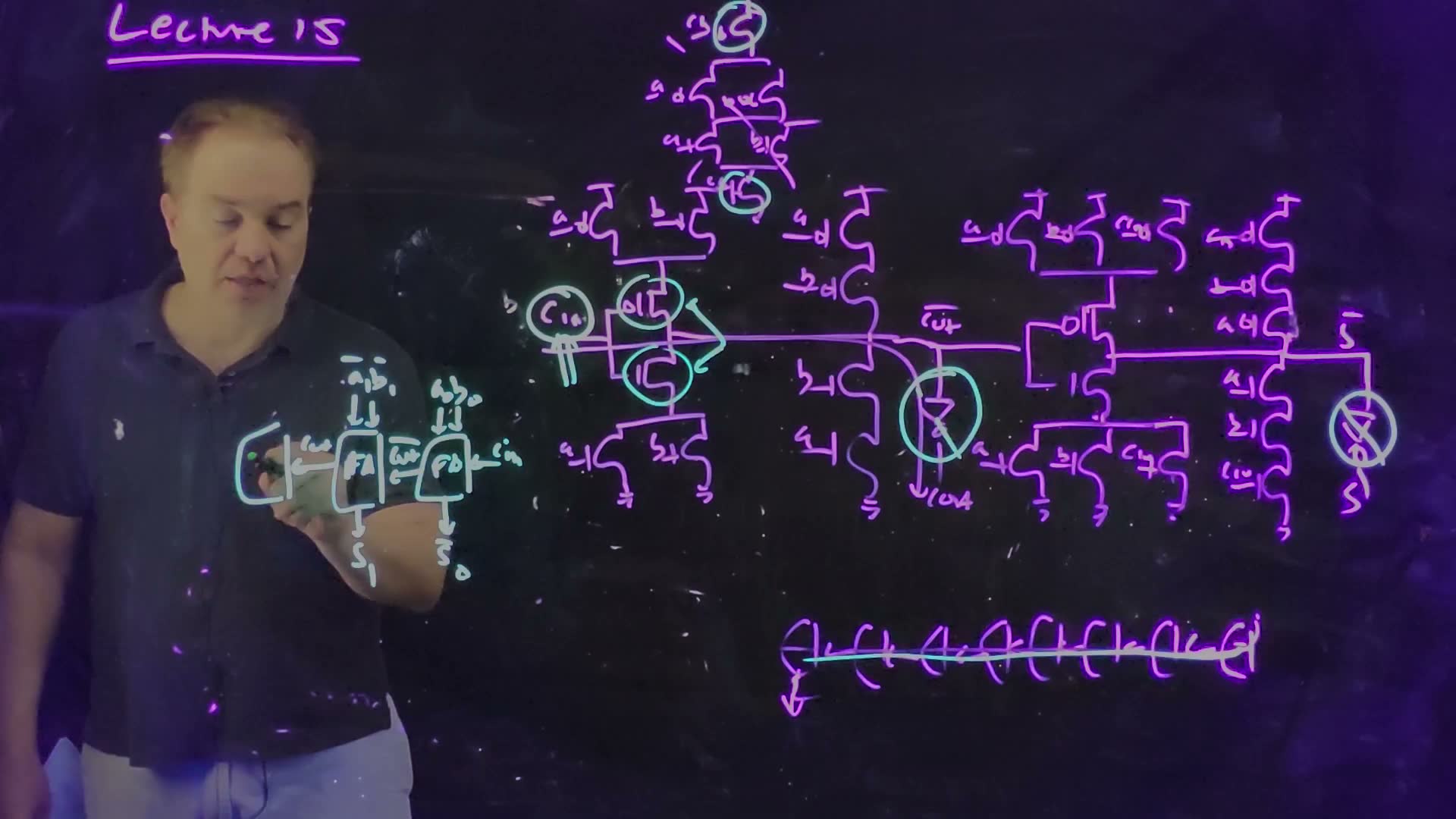
- Take the inverters out (18:11) board. The board crosses out both output inverters, the carry’s and the sum’s (both are ringed and struck out by 21:39). Bit 0, fed , and , now produces (and ).
- Feed the next bit inverted inputs (19:17–20:20) board. Bit 1 receives the inverted carry. Give it inverted operands too, and . Then all three of its inputs are complemented, and by self-duality its carry stage computes : the true carry. Its sum stage likewise gives the true .
- Alternate. Bit 2 receives a true carry, so it takes true , and gives an inverted carry and , like bit 0. Bit 3 is like bit 1, and so on: even bits take true operands and produce inverted outputs, odd bits take inverted operands and produce true outputs.
- Where the inverters went (20:20–21:10). To the operands of the odd bits, which are ready at the start of the cycle and are inverted in parallel with everything else, and to the even bits’ sums, which leave the adder. Neither is on the carry chain. “I don’t pay any penalty in having to invert the A and the B’s … So this is a win” (21:00).
The inverterless carry chain, redrawn from the board (Lecture15 @ 21:39; the board draws three bits and part of a fourth, and bit 3 completes the pattern). Even bits take true operands and pass on an inverted carry; odd bits take inverted operands and, by self-duality, pass on the true carry. The only inverters left are on the even bits’ sums, off the carry path.
The board (Lecture15 @ 21:39)
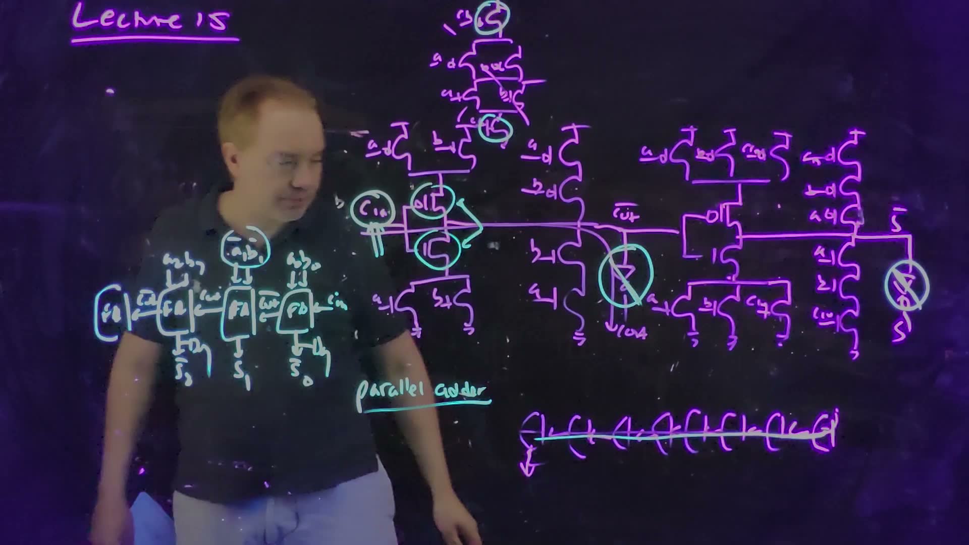
Fair copy of the board above (Lecture15 @ 21:39), mark for mark in its own layout: the last board before the lecture’s re-taped second part. Black is the violet pen: the transistor-level full adder of 18:06, unchanged, and the title; the rest of the left column is erased (a stub of the “Datapath / dataflow” underline and the lone of 09:32’s column sum remain). Teal is the cyan pen: the rings of 18:06, the strokes through both output inverters (the carry and the sum stage drop them), and the inverterless chain with “parallel adder”. Two slips are copied as written and marked †: bit 2’s inputs "" are , and its sum "" is . The lower corner of the leftmost box, under the lecturer’s hand here, is copied from 21:00. The chain’s three left bits sit a little further apart than on the board, so the carry labels fit between the boxes.
What the win is worth
The lecture says “win” without a number. Chapter 8’s gains give one added. Use §5’s sizes: the carry stage’s input is 6 units with , and its own sum stage’s input is 6 units. Leave out, for now, the next bit’s sum stage, which also reads the carry through its input; its load is the condition at the end.
Per bit, with and without the inverter (τ_inv)
- Without the inverter. Each carry node drives the next carry stage’s (6) and its own sum stage’s (6): , so the stage takes per bit.
- With an inverter of size (input units). The carry stage drives the inverter and its own sum stage: . The inverter drives the next : . Per bit, .
- The best inverter. The terms and balance where , at : . A unit inverter () gives .
- Eight bits. Inverterless: . With the best inverters (38.63); with unit inverters . Removing the inverters saves against the best, 17%.
The carry chain’s delay per bit added, computed from Chapter 8’s gains with §5’s sizes, the next sum stage’s load left out: with an inverter of size after each carry stage, (curve; least, , at ), and without it, 4 (line). No inverter size reaches the line.
Check (a bound). By the inequality of arithmetic and geometric means, for every , so : no inverter, however sized, beats the inverterless chain here. The plot shows the same: the curve never touches the line.
Memorize or derive. Derive: two gains per bit, each with the loads read off the circuit. The lesson to memorize is the lecture’s: an inverter on the carry chain is paid times.
What breaks it: the sum stage’s load. The next bit’s sum stage reads the carry too, through its input; call that load units. Without inverters it sits on the carry node: . With an inverter it sits on the inverter’s output: , least . The two are equal at (both , with ), and the inverterless chain wins exactly when : when the sum stage loads the carry less than the next carry stage does. A sum stage sized for full drive, as in §5, puts units on it (), and then the inverter wins: against at . So the lecture’s win comes with a design rule added: build the sum stage small. It is off the critical path except at the top bit, so it can afford to be slow, and a small sum stage keeps the carry wire light. FN19-3’s , “the loading of the sum circuit at each bit”, is this load: in its inverterless chain the own sum stage’s input and the next one’s input both sit on the carry node, lumped.
Traps.
- Inverting the carry but not the next bit’s operands. The next stage would then compute the majority of mixed polarities, , which is wrong.
- Forgetting the even bits’ sums. They come out inverted and still need an inverter, off the carry path but there.
Check yourself In the inverterless chain, which bits take inverted a and b?
The odd bits: 1, 3, 5, …. Bit 0 takes true operands, because it receives the true ; each bit after it receives a carry of the opposite polarity to its neighbour’s.
Check yourself FN19-3's carry chain (solved in F2, §4) has, in every stage, the carry input's device in series with one conducting device on each side, the other two inputs tied to 1 and 0. Which part of the mirror carry stage is that, and why is the stage's logical effort 2?
Step 1: with and the stage is held in propagate. The – series branch could never conduct (one of its devices is always off), so FN19-3 leaves it out; what remains is the branch, in series with the one conducting device of the ( parallel ) pair on each side. Each stage inverts its carry, as this section’s chain does. Step 2: every device is in a two-high stack, so each is twice the inverter’s width; the input drives one doubled NFET and one doubled PFET, twice an inverter’s input for the same drive: .
FN19-3 itself, with its delay, energy and best width, is solved in F2, §4.
8. Datapath layout: the bit stack
You need
Layout image (Chapter 9, §8). Each metal layer has a preferred routing direction, alternating up the stack: if M1 runs horizontally, M2 runs vertically, M3 horizontally, and so on. A route that must turn changes layer instead of blocking the layer it is on.
Design rules (Chapter 9, §6). Every layer has a minimum width and a minimum spacing. A routing track is one wire’s width plus one spacing: the pitch at which parallel wires can be packed.
The question. A datapath does the same thing to every bit of a word. How does that shape its layout?
The bit stack (board, 23:24–27:40)
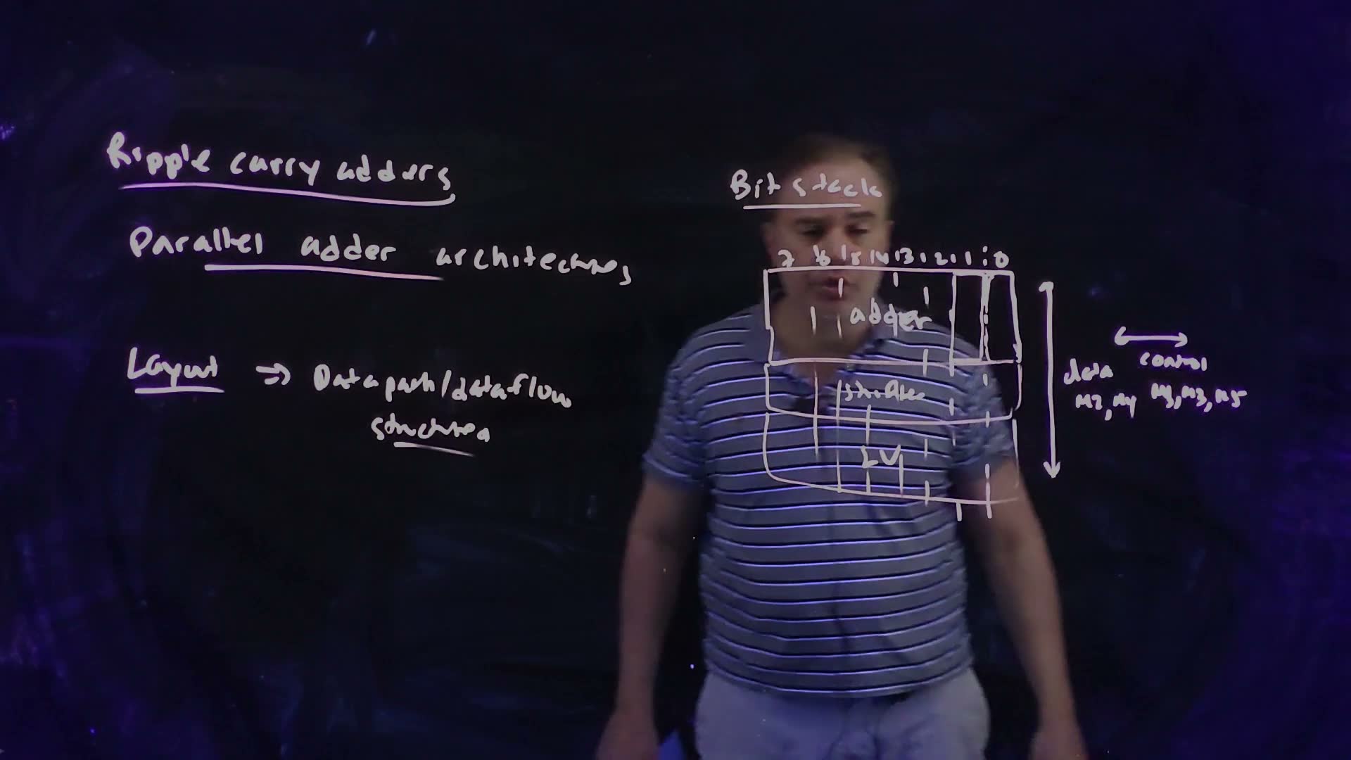
- The same circuit in every bit (23:24–24:42). Datapaths are “highly structured”, so their layouts are built as a bit stack board: each block (an adder, a shifter, a logic unit LU) is cut into identical bit slices, and the blocks are stacked so that bit of every block lies in the same column.
- Data one way, control the other (24:42–25:15) board. The data run up and down through every block, on the vertical layers M2 and M4. The control signals, which tell a whole block what to do and so are shared by all its bits, come in from the side on the horizontal layers M1, M3 and M5. That is layout image at the scale of the whole datapath.
- One bit pitch for every block (25:15–27:40) board. The width of a slice, the bit pitch, must be the same in every block. If a shifter’s slices were narrower than the adder’s, the data wires would have to jog sideways between them (the board’s crossed-wire sketch), which costs area and wiring.
- Choose the pitch first. The pitch is set early, from the number of routing tracks a slice needs, each a minimum width plus a minimum spacing (“# of routing tracks”, “minimum width”, to which the board soon adds “spacings”). A more complex block then grows taller, not wider.
A datapath as a bit stack, redrawn from the board (Lecture15 @ 27:07). Every block is cut into slices of one bit pitch, bit 7 at the left; data run vertically on M2 and M4, control horizontally on M1, M3 and M5. A more complex block is taller, not wider. Right (✗): blocks of different pitch force the data wires to jog between them.
The board (Lecture15 @ 27:07)
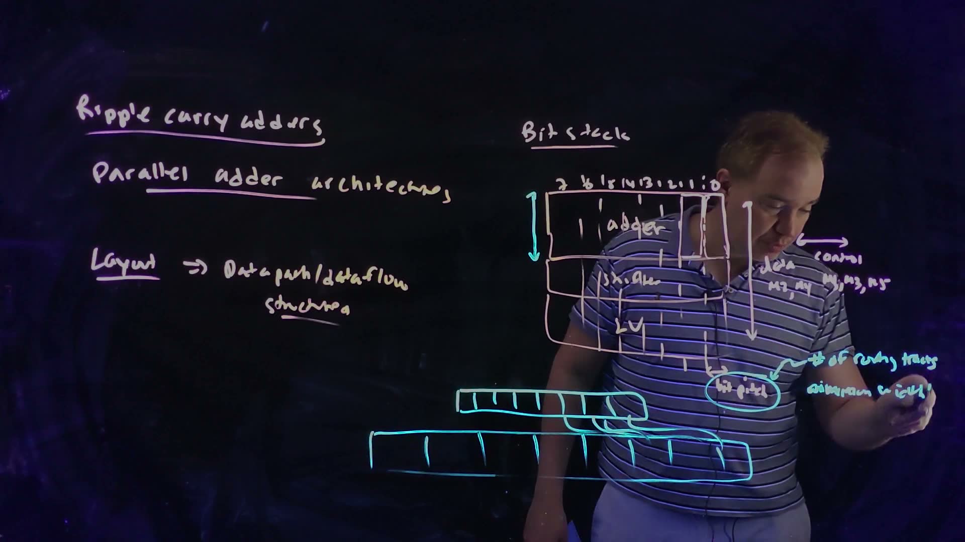
Fair copy of the board above (Lecture15 @ 27:07), mark for mark in its own layout. Black is the cream pen: the titles and the bit stack with its data and control notes. Teal is the cyan pen, which added the pitch notes over it: the arrow beside the adder, the ring round “bit pitch”, “# of routing tracks”, “minimum width” and the sketch of two rows with different pitches joined by bent wires. Two board slips are copied as written and marked †: the 5 among the bit numbers is written like an 8, and “minimum” is written “aimimum”. The stroke after “width” is the start of the “/” of “width/spacings”, which the lecturer is writing here.
The ripple-carry adder in a bit stack
The adder's slices (board, 27:58–30:55)
- Two cells per bit (27:58) board. Each bit’s slice holds a carry cell C over a sum cell S; the eight slices sit side by side.
- Shared rails and wells (28:57–29:44) board. Horizontal M1 rails run along the rows: above the carry cells, ground between the carry and sum cells, below the sum cells. The PFETs sit next to and the NFETs next to ground, so the rows read P, N (carry), N, P (sum), and the next block below shares the bottom n-well and rail.
- A power grid (29:44) board. Vertical M2 straps over the slices alternate between vdd! and gnd! (the global net names), tying the rails into a grid.
- Cells that wire themselves (29:57–30:55). With forethought, each carry cell’s carry-out lands where the next cell’s carry-in is, so the cells abut and the carry chain connects with very little extra metal: “they just connect together like a set of Lincoln Logs” (30:24).
The ripple-carry adder as a bit stack, redrawn from the board (Lecture15 @ 30:26). Each bit is a carry cell C over a sum cell S. M1 rails run along the rows (, ground, ), with the PFET rows (P) beside and the NFET rows (N) beside ground; the dashed P row is the next block’s, sharing the n-well. M2 straps alternate vdd! and gnd! to form a grid.
The board (Lecture15 @ 30:26)
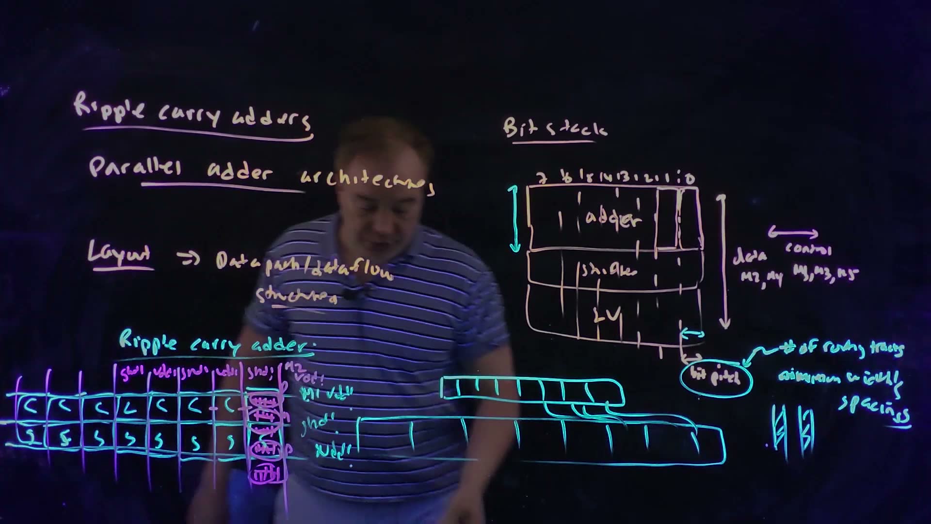
Fair copy of the board above (Lecture15 @ 30:26), mark for mark in its own layout, on the coordinates of the 27:07 copy. Black is the cream pen (the titles and the bit stack); teal is the cyan pen (the pitch notes of 27:07, then the carry and sum cells with their M1 rails, “spacings” and the hatched tracks at the right); magenta is the violet pen, which added the M2 straps and, in the eighth column, the ringed device rows: P, N for the carry cell and N, P for the sum cell, then the next block’s P row sharing the bottom rail. Two board slips are copied as written and marked †: the 5 among the bit numbers is written like an 8, and “minimum” is written “aimimum”. The strap labels are wider in type than the columns they sit in, so the vdd! labels are set one row above the gnd! labels.
Memorize or derive. Derive it from the meaning of a track. The facts to remember are qualitative: one pitch for all blocks, set first; data vertical, control horizontal; complexity goes into height.
A worked example added (illustrative values; the course gives no metal pitch). For example, with 8 M2 tracks per bit at a track pitch of 0.2 µm, the bit pitch is at least µm, and a 32-bit datapath is at least µm wide, in every block.
Trap. Choosing each block’s pitch for its own density. The blocks then do not line up, and every boundary between them needs jogs.
Check yourself In the same stack, a shifter needs 10 M2 tracks per bit and the adder 8. What bit pitch must the stack use, and where does the adder's spare room go?
Step 1: the pitch must fit the block that needs the most tracks, the shifter: 10 tracks, for example µm, and the 32-bit stack is then 64 µm wide. Step 2: the adder keeps that same pitch; its two spare tracks per bit stay free for routing, and any extra logic it has goes into its height.
Check yourself A 64-bit stack's densest block needs 12 tracks per bit, at 0.2 µm a track. How wide is the stack, and how much narrower would it be if that block were redesigned to need 10?
Step 1: the pitch is set by the densest block: µm, so the stack is µm wide, in every block. Step 2: at 10 tracks the pitch is 2.0 µm and the stack 128 µm: 25.6 µm narrower, for the whole datapath, because every block shares the pitch.
9. Parallel adders start from generate and propagate
You need
The full adder (§1): (majority), (odd parity).
The ripple’s critical path (§2). In an -bit ripple-carry adder the worst case is a carry made at bit 0 rippling through every bit’s carry circuit: the delay grows linearly with .
The question. To beat the ripple, the carries must be computed without waiting for each other. What do all the faster adders start from?
From the carry to g and p (21:10–34:50)
- Why parallel adders (21:10–21:44, and again after the seam, 22:30–22:58). They compute the carries in parallel, paying in hardware, power and area. For small adders the ripple is hard to beat: “for like 8-bit adders or so, a ripple carry adder is probably gonna be the fastest implementation” (22:58); beyond that, parallel architectures win. The lecture shows two “historical” ones first, carry bypass and carry select (34:25), then carry lookahead, “the way these adders are really done”.
- Rewrite the carry (32:17–32:52) board. Factor out of two terms of the majority: . Name the pieces: , the generate, and , the propagate. Then .
- What the names mean (32:52–33:24). If (both bits 1), the bit makes a carry whatever is: it generates one. If and , the bit passes through: it propagates it. If both are 0, : the bit kills the carry.
- Two choices of propagate (33:24–33:54) board. or . They differ only at , and there already makes . So the carry comes out right with either.
- Only gives the sum (34:00–34:22). With , the sum is : one more XOR. With it fails at , : the true sum is 0, but . “That’s a very important idea that students often get confused about” (34:22). From here on, .
| 00 | 0 | 0 | 0 |
| 01 | 0 | 1 | 1 |
| 10 | 0 | 1 | 1 |
| 11 | 1 | 1 | 0 |
The PG cell and the carry and sum from it added (equations from Lecture15 @ 33:43 and 34:50). Left: one AND and one XOR turn , into and . Right: and . Every parallel adder keeps the left half for each bit and replaces the right half’s carry by something faster.
The board (Lecture15 @ 33:43)

Fair copy of the board above (Lecture15 @ 33:43), mark for mark in its own layout. One pen wrote the whole board, so the copy is all black. Nothing on the board is hidden: the lecturer’s hand is below "", and both lines for are whole. Faint remnants of the wiped bit-stack board are left out.
Memorize or derive. Memorize all four, with the condition: the carry works for either propagate, the sum only for . The derivation is one line: factor out of the majority.
A worked example added. : , ; and , so the bit writes 11, which is . With instead, the sum would come out , wrong.
Trap. Computing because an OR is cheaper than an XOR, and then using it for the sum (or, §10, for a bypass).
Check yourself For which inputs do a + b and a ⊕ b differ?
Only for , where the OR is 1 and the XOR is 0.
Check yourself A bit has g = 0 and p = 1, and its cin rises from 0 to 1. What do cout and s do?
Step 1: , so it follows, 0 to 1: the bit propagates. Step 2: , so it falls, 1 to 0.
10. Carry bypass
You need
Propagate (§9). A bit with passes its carry-in straight to its carry-out ( is then 0). A group of bits that all have passes its carry-in through all of them.
A 2:1 multiplexer (mux; Chapter 10, §7 builds them). Two data inputs and a select: the output copies one input or the other, chosen by the select.
The ripple’s critical path (§2): a carry made at bit 0, rippling through every bit; to the top sum.
Stage delays added, all in : is one carry stage’s delay (carry-in to carry-out), one sum stage’s, one 2:1 mux’s and one PG cell’s.
The question. If a whole group of bits propagates, its carry-out is simply its carry-in. Can a wire around the group skip the ripple?
The bypass adder (board, 35:16–38:50)
- One group (35:16–36:29) board. Take a 4-bit group of the ripple adder. If to are all 1, the carry-in will reach the group’s end anyway, through four carry circuits. A mux at the group’s end chooses between the rippled carry-out and the group’s carry-in, carried around the group on a bypass wire; its select is board. When the carry skips the group in one mux delay.
- Sixteen bits (36:29–37:21). Four groups, each with its bypass mux; the last group’s mux gives .
- The critical path (37:21–38:24). A carry that bypasses everything is fast. The slow case starts and ends with a ripple: a carry generated at bit 0 cannot bypass group 0 (with , , so ). It ripples through group 0’s four bits and passes group 0’s mux; groups 1 and 2 propagate fully, so it bypasses each in one mux delay; then it ripples through group 3 to the top sum .
- The lecturer’s count (38:24): “two ripples through four, and then two mux delays”, against sixteen carry stages. The careful count added adds two details: the path also passes group 0’s mux (the board draws one there), and in group 3 the carry into bit 15 needs only three carry circuits ( to ), then the sum. With the PG cells first (the select needs the , and the carry cells use , ), the path is .
- “Historical” (34:25). Bypass adders are rarely used now, but finding their critical path is the reasoning every faster adder needs.
A 16-bit carry-bypass adder, redrawn from the board (Lecture15 @ 38:48). Each 4-bit group has a mux that passes the group’s carry-in straight on when every bit propagates (); the last one gives . The bypass wires, which the board runs under the groups, are drawn as arcs over them; the board’s own violet arcs mark the critical path. The thick line is the critical path: generated at bit 0, rippling through group 0, through its mux, bypassing groups 1 and 2, and rippling through group 3 to .
The board (Lecture15 @ 38:48)
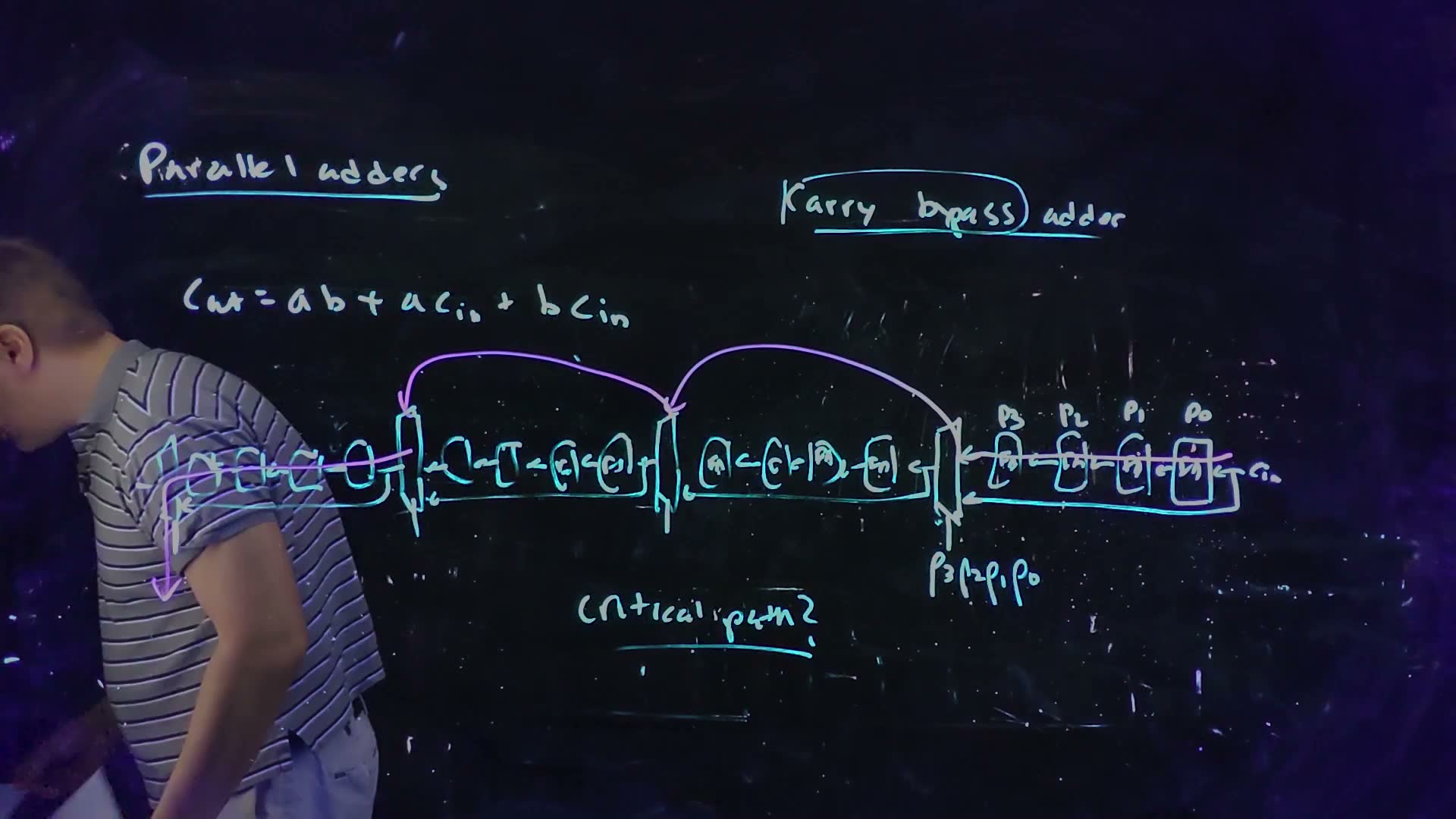
Fair copy of the board above (Lecture15 @ 38:48), mark for mark in its own layout. Black is the cyan pen, which drew the adder: four groups of four full adders with a mux at the end of each group, fed by the group’s rippled carry and by its carry-in on the wire under the group. Magenta is the violet pen’s critical path: rippling through the first group, then along two arcs from mux to mux over the second and third groups, then rippling through the last group to the top sum. The board’s tiny FA labels inside the boxes are left out. The title’s first letter is written like a K (†): read “Carry”. The left end, dimmed behind the lecturer here, is read from 38:25.
Memorize or derive. Derive it by tracing: ripple out of the first group, one mux per group after that up to the last, ripple into the top bit, one sum.
A worked example added. Take, for example, and . Sixteen bits in groups of 4: , against the ripple’s . The lecturer’s round count, , gives .
The carry-out added. The same carry, generated at bit 0, reaches through all four muxes, with no ripple at the end: , sooner than . The top sum, not the carry-out, sets the clock.
Why the select must use added. The lecture allows “A or B, or A XOR B” (35:30); for a bypass, only XOR works. Take , , . The true sum is 23, binary 10111, so the group’s carry-out is 1 (bit 3 generates it). With OR-propagate every bit has , so , and the mux passes the carry-in, 0: wrong. With XOR-propagate, , so , and the mux takes the rippled carry, 1: right. A group with under XOR has no generating bit, so its carry-out really is its carry-in.
Traps.
- Counting only the skipped groups’ muxes. The path also passes the first group’s mux: three muxes for four groups.
- Taking the bypass path as the critical one. A carry that bypasses every group is the fast case; the slow one starts and ends with a ripple.
Check yourself Which input pattern makes group 1 (bits 4–7) bypass its carry?
: in each of bits 4 to 7 exactly one of , is 1 ().
Check yourself With the example delays, how long does a 64-bit bypass adder in groups of 4 take, and how does that compare with a 64-bit ripple adder?
Step 1: muxes, so . Step 2: the ripple takes . The bypass is still linear in (one mux per group), but with a slope of per four bits instead of per bit.
11. Carry select
You need
PG and the sum (§9): , , and the sum , where is the carry into bit .
A 2:1 multiplexer (Chapter 10, §7): the select picks one of two inputs.
Critical-path reasoning (§10). Follow the slowest signal through the blocks, counting each block it must wait for once; blocks that work at the same time count once together.
Stage delays added, all in : is one carry stage’s delay (carry-in to carry-out), one sum stage’s, one 2:1 mux’s and one PG cell’s.
The question. Instead of waiting to learn a group’s carry-in, compute the group’s carries for both possible carry-ins in advance, and choose when the real one arrives. How fast is that?
The select adder (board, 39:24–43:26)
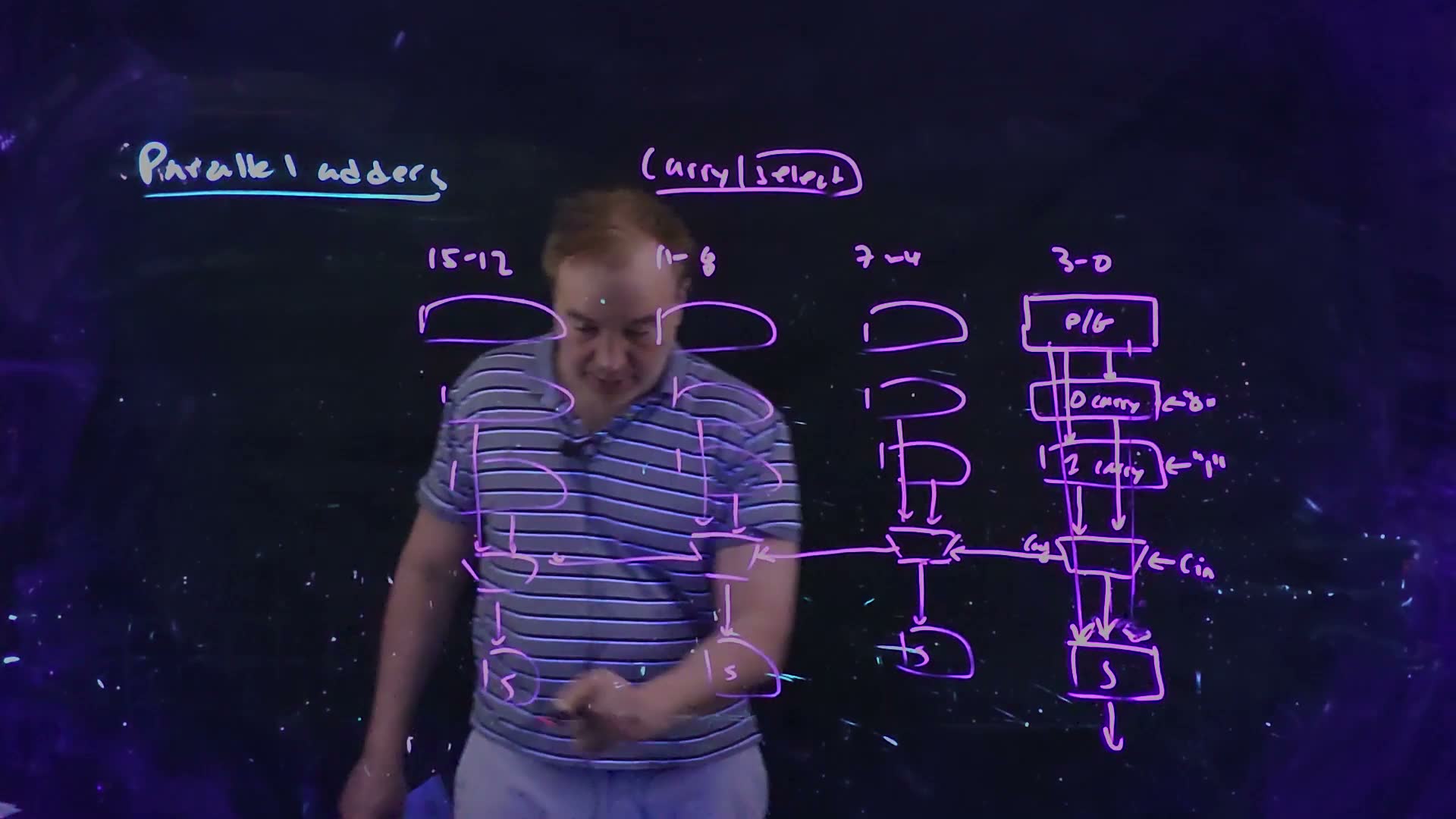
- One bin of four (39:24–40:30) board. Bits 3–0: a PG generator, then two carry chains fed the same , : the “0 carry” chain assumes a carry-in of 0, the “1 carry” chain a carry-in of 1.
- Select (40:30–41:29) board. A mux on the real picks one chain’s carries. This is speculation: half the work is thrown away, “hence the name select”.
- The sums (41:29–41:49). The sum generator needs only the and the chosen carries (“I don’t need the G’s”), because gives (§9).
- Sixteen bits (41:49–42:42) board. Bins 7–4, 11–8 and 15–12 repeat the bin. Each bin’s carry-out, from its mux, is the select of the next bin’s mux; the last mux gives .
- The critical path (42:42–43:26). All the bins’ chains run at the same time, right after PG. Then the muxes work in series: bin 0’s mux on , then bin 1’s on bin 0’s carry-out, and so on. So: PG, one 4-bit chain, four muxes, and the top bin’s sum.
A 16-bit carry-select adder, redrawn from the board (Lecture15 @ 43:39). In every 4-bit bin, two carry chains compute the carries for a carry-in of 0 and of 1, at the same time; a mux, selected by the previous bin’s carry-out, picks one set, and the sum box forms . The thick line is the critical path: PG, one chain, the four muxes in series, and the top bin’s sum.
The board (Lecture15 @ 43:39)
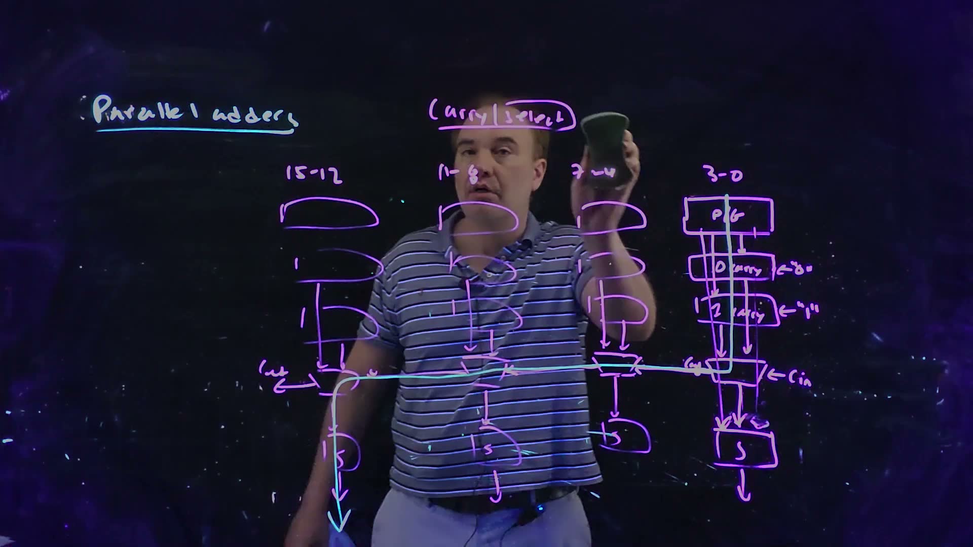
Fair copy of the board above (Lecture15 @ 43:39), mark for mark in its own layout. Black is the violet pen: the bins, their blocks (boxes in bin 3–0, D shapes in the others), the muxes and the select chain, and the pale title. Teal is the cyan pen: the title’s underline and the critical path, added last, from bin 3–0’s P/G down into its mux, along the select chain and down through bin 15–12. Two slips are copied as written and marked †: the 1 of “1 carry” is drawn with a hook and reads like a 2 (the quoted input “1” and the speech at 40:14 settle it as 1), and the carry-out at bin 3–0’s mux is written “Cay” for . Bin 7–4’s upper blocks, washed out by the lecturer’s raised hand here, are copied from 42:40, as is the select wire under the cyan path.
Memorize or derive. Derive by tracing: one chain (they all run at once), then every mux (they run in series), then one sum.
A worked example added (the same example delays as §10: , ). Sixteen bits in bins of 4: , against bypass 46 and ripple 64. At 64 bits: , and now the chain of 16 muxes is 64 of those 86. The mux chain is linear in ; a tree (§13) avoids it.
Trap. Counting bin 0’s mux as free because is known early. The mux still has to wait for bin 0’s chains to finish before it can pass their carries on.
Check yourself How much hardware does carry select add to a ripple adder, per bin, and what does it buy at 16 bits with the example delays?
Step 1: per bin, a second carry chain and a mux (and the PG cells, if the ripple’s full adders did not have them). Step 2: at 16 bits the delay falls from to , for roughly twice the carry hardware.
Check yourself At 64 bits the bin size M is free. With the example delays, which M makes tPG + M tc + (N/M) tmux + tsum smallest, and what is the delay?
Step 1: bigger bins lengthen the one chain on the path () but shorten the mux chain (); the sum of the two is least where they are equal, , so . Step 2: , against 86 with bins of 4 (and 86 again with bins of 16).
12. Carry lookahead: unrolling the carry
You need
Generate, propagate and the carry (§9). For bit : (the bit makes a carry), (the bit passes its carry-in on), and the bit’s carry-out is times its carry-in. The sum is XOR the carry into the bit.
Carry numbering (this section and §13). is the carry into bit : , bit 0’s carry-out is , and bit ‘s carry-out is . So , and a 4-bit group’s carry-out is .
The question. Each carry depends on the one before it, which is why it ripples. Can we write every carry directly from the ‘s, ‘s and , so that all of them are computed at once?
Unrolling (board, 44:10–47:59)
-
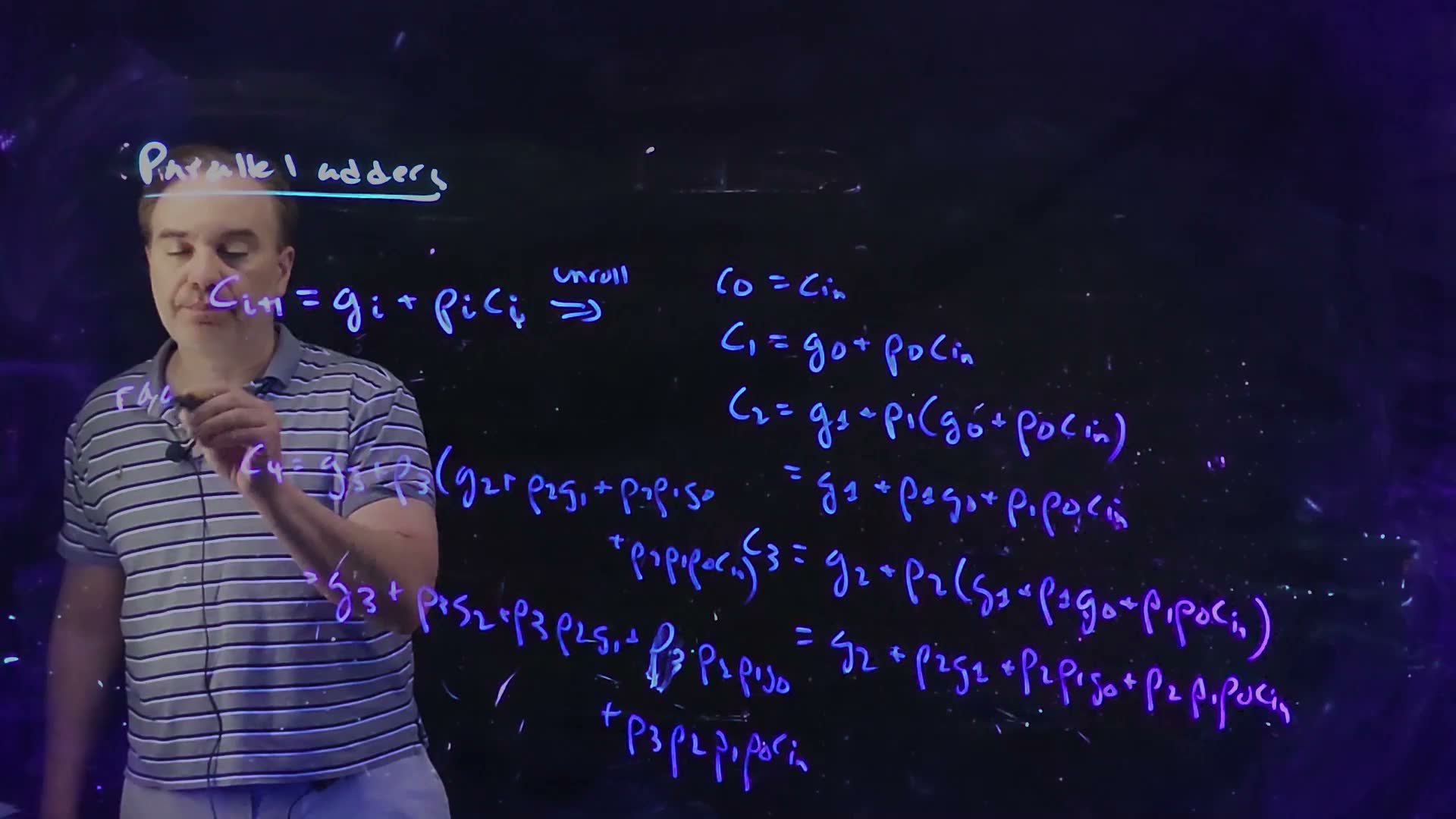
The recursion (44:10–44:52) board. In the new numbering, bit ‘s carry-out is . Each carry needs the one below it: that is the ripple.
-
Substitute (44:58–46:49) board, “⇒ unroll”. Put each carry into the next:
Every carry is now a sum of products of the ‘s, ‘s and : two levels of logic, with no carry waiting for another. Four bits at a time is called radix 4 board.
-
Read each line in words. is 1 if bit 3 generates; or bit 2 generates and bit 3 propagates; or bit 1 generates and bits 3 and 2 propagate; or bit 0 generates and bits 3 to 1 propagate; or is 1 and all four bits propagate. Each term is “a carry made here, passed by everything above”.
-
Group generate and propagate (47:15–47:59) board. Each line has the shape . The board braces them for : and ; for : and . The group generate says the group makes a carry by itself; the group propagate says it passes through. They are and again, one level up.
The board (Lecture15 @ 48:01)

Fair copy of the board above (Lecture15 @ 48:01), mark for mark in its own layout. All black: one blue pen wrote the board (the title and its underline are left from 33:43). ’s lines lie over the lecturer’s striped shirt here, which washes them out; their terms are read on 47:09, where they are clear, and the G bracket over the second line and the start of the P bracket under the last, new at 48:01, on a frame at 48:15. Two slips are copied as written and marked †: "" for and "" for . The fourth term’s is written over a first attempt. The lines are levelled; on the board they drift down to the right.
Groups of four, and groups of groups
For the four bits added (the bit range in the subscript, high index first):
The smallest case is two bits added: with and . Read the formula with “bit 1” and “bit 0” replaced by “the upper group” and “the lower group”: the pair generates if the upper part generates, or the lower part generates and the upper part propagates; it propagates if both parts do. That is the radix-2 element:
It combines any two adjacent groups, of any size, into one. Two 2-bit groups give the 4-bit group: , which is term by term, and . And the carry-in can join as a group of its own below bit 0, with : it “generates” exactly when and passes nothing through. Combining bit 0 with it gives : the carry into bit 1. So the carry into any bit is the group generate of everything below it, the carry-in included. Chapter 17’s radix-2 trees, and FN17-8’s adder, are networks of this one element.
The radix-2 element added. Main: it combines an upper group and the adjacent lower group into one group. Middle: applied to two bits, it gives the two-bit group terms of the board’s . Right: with the carry-in entered as the group , it gives the carry and a propagate of 0 (the box’s equations are written inside it).
Memorize or derive. Memorize the recursion and the radix-2 element. Derive to by substitution (three lines), and , by reading off the coefficient of .
A worked example
An added example added: (11), (6), .
| bit | 3 | 2 | 1 | 0 |
|---|---|---|---|---|
| 1 | 0 | 1 | 1 | |
| 0 | 1 | 1 | 0 | |
| 0 | 0 | 1 | 0 | |
| 1 | 1 | 0 | 1 | |
| (into bit ) | 1 | 1 | 0 | 0 |
| 0 | 0 | 0 | 1 |
1011 + 0110 by lookahead
- PG. Because every carry formula needs only and : and .
- The carries, each from its unrolled formula. . , since . . . None waited for another.
- The sums. : 1, 0, 0, 0 from bit 0 up, so , and . The answer is binary 10001, which is 17, and .
- The group terms. (the group makes its own carry, at bit 1, and bits 2 and 3 pass it) and (bit 1 does not propagate). So whatever is.
A second case, all-propagate: , , . Then and , so and : the group passes straight through. Every carry is 1, and : binary 10000, which is 16, and .
Check. The ripple of §2 gives the same carries bit by bit: in the first example bit 0 adds (no carry), bit 1 adds (carry), bit 2 adds (carry), bit 3 adds (carry): , as in the table. (The page’s test compares the two on all 512 inputs of a 4-bit adder.)
Traps.
- Off by one in the carries. is the carry into bit , so and is the 4-bit group’s carry-out. Wiring from shifts every sum one place. Past papers number bits differently (FN17-8 counts its bits from 1, with the carry-in at position 0), so settle the numbering before wiring a sum.
- Putting inside . is the coefficient of , , as the board’s brace marks it (the brace stops at ), so that the carry is . Fold into and the group no longer combines with its neighbour by .
Check yourself Write c3 fully unrolled.
: a carry made at bit 2, or at bit 1 and passed by bit 2, or at bit 0 and passed by bits 1 and 2, or the carry-in passed by all three.
Check yourself An 8-bit group is two 4-bit groups. Write G7:0 and P7:0 with the radix-2 element, say in words when the 8-bit group generates, and evaluate it for (G7:4, P7:4) = (0, 1) and (G3:0, P3:0) = (1, 0).
Step 1: and : the byte generates if its upper half generates, or its lower half generates and every bit of the upper half propagates. Step 2: and : the carry made in the lower half passes through the upper half, so the byte’s carry-out is 1 whatever its carry-in.
Check yourself Start from the carry-in as the group (cin, 0) and apply the radix-2 element twice, first with bit 0 and then with bit 1. What do you get, and what does the order of the combinations do to the delay?
Step 1: with gives ; then with gives , the board’s . Step 2: combined one bit at a time like this, the elements form a chain, one after another: the ripple again. A tree (§13, Chapter 17) combines the same pairs in a different order, so that each carry passes far fewer elements.
13. The radix-4 lookahead unit and the tree adder
You need
Group generate and propagate (§12). Four bits’ carries can be computed at once from their , and the carry-in: up to , with (the group makes a carry) and (the group passes ). The same formulas work with groups in place of bits.
The PG cell and the sum (§9): each bit makes and , and, once its carry is known, .
Stage delays added, all in : is one carry stage’s delay (carry-in to carry-out), one sum stage’s, one 2:1 mux’s and one PG cell’s; is the delay through one lookahead unit.
The question. Lookahead computes four carries at once. How do we build a 16-bit or 64-bit adder from it without rippling again?
From one unit to a tree (board, 48:52–54:50)
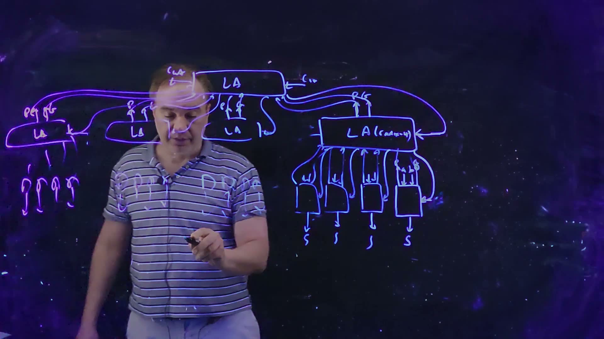
- The radix-4 lookahead unit (48:52–50:44) board. One block, “LA (radix-4)”, holds §12’s logic. Below it sit four cells, one per bit. Each cell takes , and sends , up to the LA; the LA sends each cell its carry back down; the cell gives . For four bits the critical path is: PG in the cells, the LA, the sum in the cells.
- Sixteen bits, rippled (50:44–51:38) board. Four units in a row, each unit’s into the next unit’s carry-in. It works, but each unit must wait for the one before: the carry ripples again, four bits at a step. “Not great”.
- A second level (51:38–53:15) board. Each first-level unit can also give its group’s and , which do not depend on its carry-in. Put one more LA unit, the same logic, over the four: it takes the four groups’ and and returns the group carries , , and , all at once, exactly as the first level returns bit carries.
- The critical path (53:23–54:07). , into the cells (PG); up to the first level (, ); up to the second level (group carries); back down to the first level, which now has its carry-in and makes the bit carries; down to the cells (sums). This is a tree, radix 4: a tree adder.
- Counting the LA delays added. Rippled units put LA delays on the path. A tree of levels puts : up through levels, then back down through (the top level’s carries go straight out). Sixteen bits: rippled 4, tree 3. Sixty-four bits: rippled 16, tree 5. The tree’s count grows with .
- What comes next (54:07–54:50). Radix-2 trees, Brent–Kung and Kogge–Stone, built from §12’s two-group element: the next lecture (Chapter 17).
A radix-4 lookahead unit over its four cells, redrawn from the board (Lecture15 @ 51:37, as first drawn at 50:17). Each cell sends its , up (labelled on bit 0); the LA returns the carries to (and ) all at once; each cell then forms . The carry labels are added.
Sixteen bits from four lookahead units in a row, redrawn from the board (Lecture15 @ 51:37). Each unit waits for the carry-out of the one before it: the thick line is the rippled path through , , to (labels added), one LA delay per four bits.
The board (Lecture15 @ 51:37)
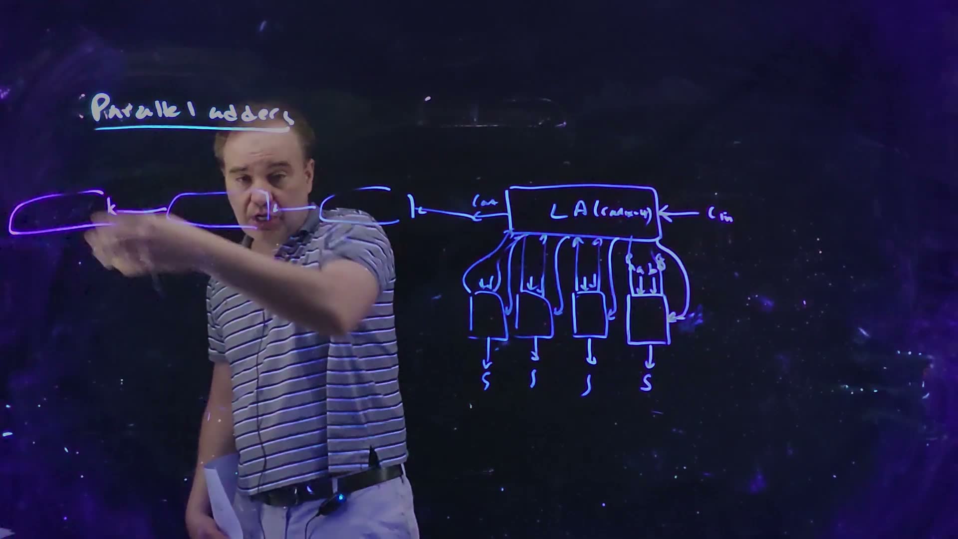
Fair copy of the board above (Lecture15 @ 51:37), mark for mark in its own layout. All black: one blue pen wrote the board (the title and its underline are left from 33:43). The three blocks at the left are the rippled lookahead units, still unlabelled; the lecturer’s arm crosses them here, and every stroke matches 53:45, where he stands clear. Only the right cell is labelled on the board (“p a b g”).
A 16-bit radix-4 lookahead tree, redrawn from the board (Lecture15 @ 53:45; the labels , , are added, and the top unit is drawn wide, with straight wires, where the board draws it narrow with curves). The first-level units send their groups’ , up; the second-level unit returns the group carries; each first-level unit then makes its bit carries. The thick line is a critical path: PG, up two levels, down one, and the sum: three LA delays.
The board (Lecture15 @ 54:50)
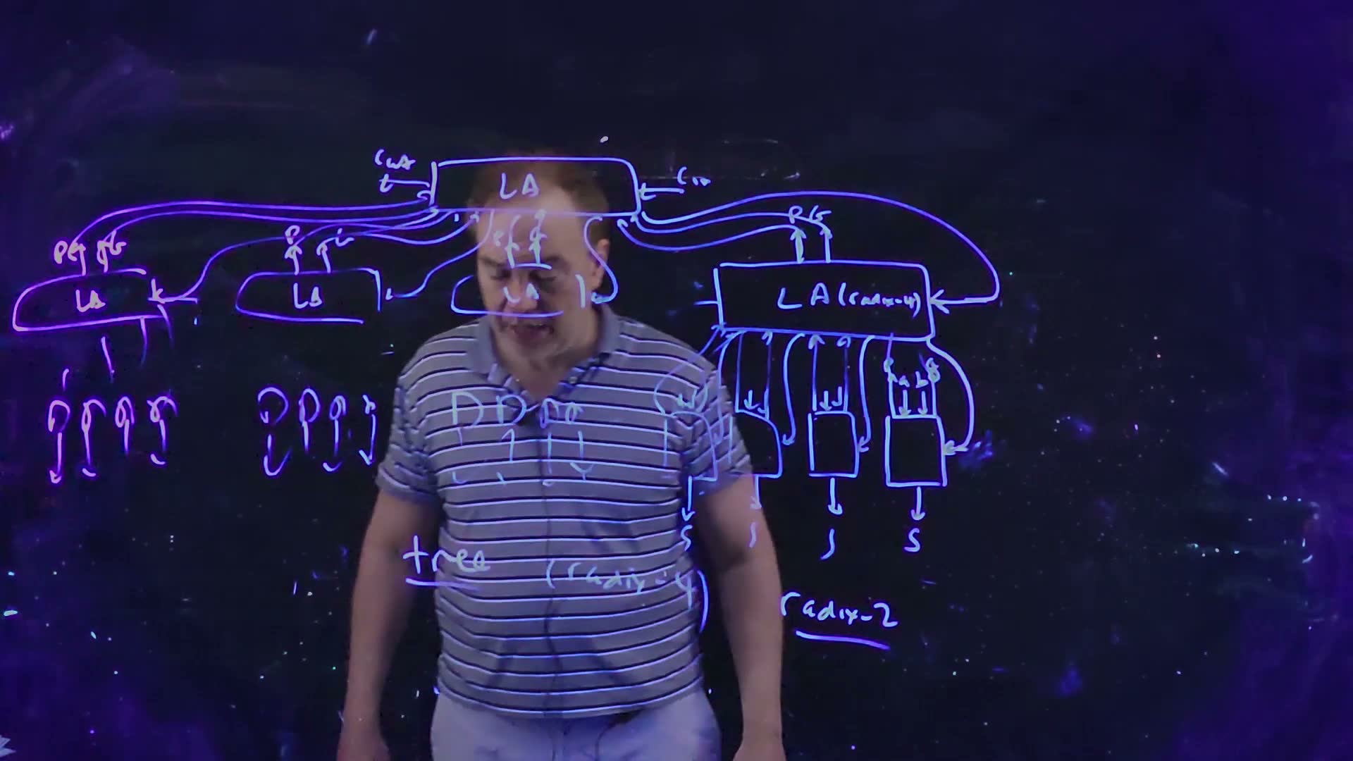
Fair copy of the board above (Lecture15 @ 54:50), mark for mark in its own layout: the 51:37 board grown into a tree. All black: one blue pen (it looks violet towards the left edge, where the light shifts its hue). The title, the ripple arrows between the blocks, and the radix-4 unit’s own and are erased by now; the unit keeps a stub of its wire. The lecturer stands in front of the middle, and his shirt washes out the strokes there: the curves above the third block and the right unit’s left cell are copied from 53:45, where they are clear. The board writes each pair “PG”; they are set as and .
Memorize or derive. Derive both by tracing the board’s path: up levels for the group terms, down for the carries. What to memorize is the shape: rippled units are linear in , a tree is logarithmic.
Comparing the five adders
An added comparison added, with the same example stage delays as §10 and §11 (, ) and, for example, (a radix-4 unit is a two-level gate with up to five-input terms, so slower than one carry stage). These are illustrations of the path counts, not the course’s numbers.
| Adder | Critical path | 8 bits | 16 bits | 64 bits |
|---|---|---|---|---|
| ripple | 32 | 64 | 256 | |
| bypass (groups of 4) | 38 | 46 | 94 | |
| select (bins of 4) | 30 | 38 | 86 | |
| LA units rippled | 26 | 46 | 166 | |
| radix-4 tree | 36 | 36 | 56 |
The five adders’ critical paths added, computed from the path counts with example stage delays , and . RCA: ripple carry; CBA: carry bypass; CSA: carry select (not the carry-save adder of multipliers); LA×4, LA×16: lookahead units rippled. Left, 16 bits; right, 64 bits. The tree pulls away as grows; the others are linear in .
What the numbers say. At 16 bits the tree is fastest (), with select close behind (38). At 64 bits the tree takes 56 against 86 for select and 256 for ripple: logarithmic against linear. At 8 bits all five are within a few stage delays of each other (26 to 38), and which one wins depends on the stage delays assumed. That is where the lecturer places the ripple’s limit, “8-bit adders or so”; the example numbers neither confirm nor contradict that rule of thumb.
Check. Count the LA units on the tree’s thick path: the rightmost first-level unit, the second-level unit, the leftmost first-level unit. Three, which is with .
Traps.
- Counting the tree’s levels once. The carries come back down through the first level: LA delays, not .
- Using the second level’s carries as bit carries. They are group carries (, , ); the first-level units still turn them into the carries of each bit.
Check yourself How many radix-4 lookahead units does a 64-bit tree need, and how many levels?
16 units over the bits, 4 over those, 1 at the top: 21 units in 3 levels.
Check yourself With the example delays, at what width does the radix-4 tree first beat the ripple adder: 4, 8 or 16 bits?
Step 1: at 4 bits the tree is one unit: , and the ripple : a tie. Step 2: at 8 bits the tree needs two levels, , against the ripple’s 32: slower. At 16 bits the tree still has two levels, 36, against 64: it wins from 16 bits.
On the exam
Adders carry little direct weight in the past finals. One part is new to this chapter, FN17-8 (15 points), which it shares with Chapter 17; the others are already solved elsewhere in the guide, and this chapter supplies the adder background they lean on.
| Part | Points | What it asks | Sections |
|---|---|---|---|
| FN17-8 | 15 | an 8-bit parallel adder built from PG generators, radix-2 lookahead elements and sum generators, and its critical path | §9, §12 (the radix-2 element and the entry), §13; the prefix network in Chapter 17 |
| FN19-3a–d | 39 | a static ripple-carry chain: delay, energy, best width | §7 (it is this chain, held in propagate), §5 |
| FN12-10b | 9 | a full adder in NP domino, | §4 (the sum identity), §1 |
| MT24-5a | 15 | the Sum and Carry of a dynamic full adder | §1, §4 |
| MT23-2b, HW4-3b | 16, — | carry and XOR in pass-transistor and CPL logic | §1 |
FN17-8 is solved, with its own figure and key, on the datapath practice page (FD1). What this chapter prepares: the three kinds of block are §9’s PG cell, §12’s radix-2 element and §9’s sum ; the carry into each bit is the group generate of everything below it, with the carry-in entered as (§12); and the critical path runs up the network and out through a sum (§13). Chapter 17 adds the radix-2 network itself. At the finals’ pace of 0.7–0.9 minutes a point, it is a 10–14 minute part.
Memorize.
- (majority) and (odd parity).
- Self-dual: ; both outputs have it, so each gate’s pull-up can mirror its pull-down. .
- The late input, , goes next to the output.
- , (not , for the sum or a bypass); ; .
- , with the carry into bit ; two groups combine as .
- Each architecture’s critical path in words: ripple (every carry), bypass (ripple, muxes, ripple), select (one chain, every mux), tree (up, down, sum).
Derive (with the path).
- The unrolled carries. Substitute into itself three times; read and as the terms without and with .
- The radix-2 element. The two-bit case , with groups in place of bits.
- The carry chain per bit. Gains from the loads: without inverters ; with an inverter of size , ; the next sum stage’s load decides.
- The critical-path counts of ripple, bypass, select, rippled lookahead and the tree, by tracing.
Method card. The playbook’s adder-architecture card: recognize a block diagram of PG, lookahead and sum blocks, or “draw the critical path”; moves PG, then carries as , then sums , marking the path up and down the tree; traps, the carry index and .
The lecture’s boards
The boards of Lecture 15 used in this chapter (25 frames)