12. Domino sizing and delayed reset
Lecture 11 built domino logic and claimed it was fast. Lecture 12 puts a number on that claim with the tool of Chapter 8: a dynamic stage carries no PFETs on its inputs, so its logical effort is below one, two thirds with a footer and one third without. It then sizes a domino gate by gain, exactly as for static CMOS, and attacks the two costs that remain. The inverter after every stage can go if n-type and p-type stages alternate (NP, or zipper, domino). The footer can go if each stage’s clock resets a little later than the one before (delayed reset). At 23:15 the lecture turns to latches and flip-flops; that is where the midterm material ends, and where this chapter stops.
After this chapter you can:
- find the logical effort of a dynamic stage, footed or footless, n-type or p-type, in either technology convention ( or equal strengths);
- size a domino gate backwards from its load for a chosen gain per stage, with a skewed inverter, as the lecture does (5.6 µm, 0.7 µm, 2.1 µm for 50 fF);
- compute the logical effort of a skewed inverter or gate on the edge that carries the logic, and compare a domino gate’s delay with the static gate it replaces;
- explain NP (zipper) domino: the p-type stage, its pre-discharge and evaluate devices, why alternating polarities removes the race, and what it costs;
- read the function and estimate the delay of a p-type dynamic stage (MT23-3, MT24-5);
- explain why a footless stage collides on an ordinary clock, how a delayed-reset clock prevents it, and why the delays eventually run out of precharge time.
Boxes and equations marked board were written in the lecture. Parts marked added are explanations or examples this guide adds.
Before you start
You need these ideas from earlier chapters. Each is restated here.
- The normalized inverter (Chapter 8). A gate’s gain is the capacitance it drives divided by the input capacitance of the inverter with the same drive. Its logical effort is its own input capacitance divided by that inverter’s input; ; gain ; a path’s delay is . The balanced inverter is 2W/W (input ), or W/W (input ) when a problem says the NFET and PFET have equal strength.
- The stack rule (Chapter 7). equal devices in series act as one device times narrower. Loads are written as widths: a load is µm of gate.
- Equal gains (Chapter 8). With fixed, the delay is smallest when every stage has the gain . Size backwards from the load.
- The domino stage (Chapter 11). A clocked precharge PFET charges the dynamic node X to while clk = 0; while clk = 1 an NFET network discharges it or leaves it floating. The clocked NFET at the foot (the footer, evaluate or foot device) prevents a collision when precharge begins with the network still on. An inverter follows; its output Y is the function, and a weak half latch usually holds X.
- The race (Chapter 11). A dynamic node fed straight into the next dynamic stage is 1 after precharge, so it starts discharging the next stage before it has decided. The domino inverter makes every precharged output 0.
- The skewed inverter (Chapter 11). All logical transitions are on one edge (X falls, Y rises), so the inverter’s PFET is made strong and its NFET weak. A strong-PFET inverter switches at a higher input voltage, which shrinks the dynamic node’s high noise margin (Chapter 6).
Notation. X is the dynamic node of an n-type stage and Y its domino output, as in Chapter 11. Sizes such as “2/1” mean a PFET 2 µm and an NFET 1 µm wide. n-type: NFETs evaluate, the node is precharged to 1. p-type: PFETs evaluate, the node is pre-discharged to 0 (the board’s word). is the complement of the clock. “Strength” is drive: a PFET has half an NFET’s strength at the same width when .
1. The domino stage and the edge that matters
The idea. In a domino stage only one transition carries the logic: the dynamic node falling, then the inverter’s output rising. The precharge PFET is not on that path at all, so it can be small.

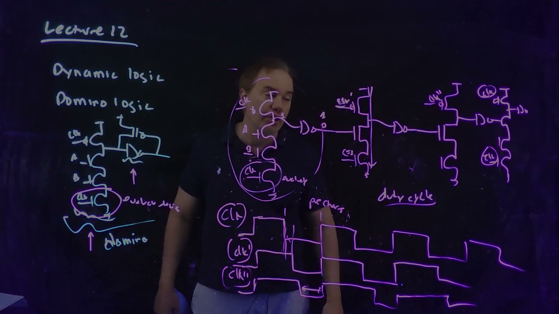
The lecture opens with the domino stage of Lecture 11 (00:06) board: a precharge PFET on the clock, the logical inputs, a footer on the clock, an inverter, and “usually a half latch here for noise considerations” (00:33). It is non-inverting. The question for this lecture: what does dynamic logic bring to delay? Logical effort answers it (00:47).
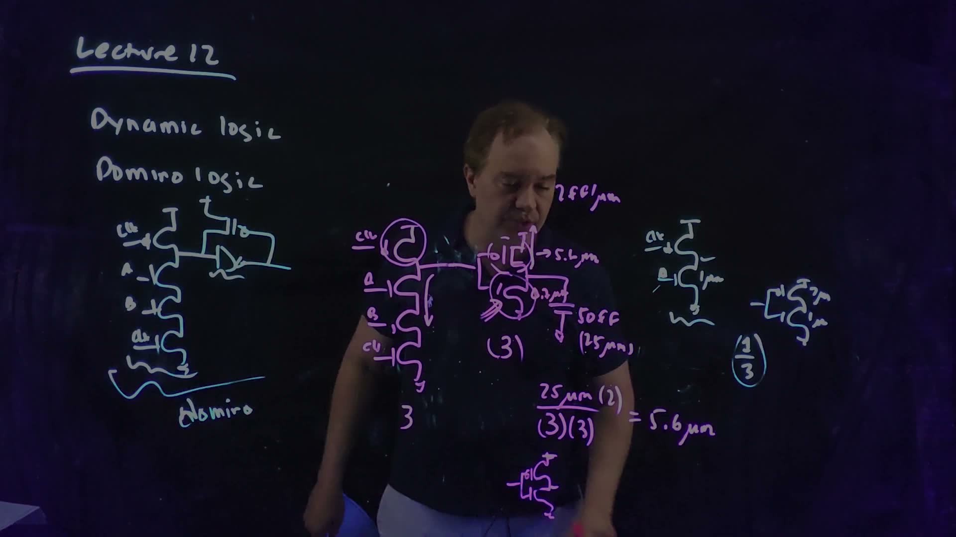
A domino gate is really two stages, the dynamic stage and the inverter (01:19). Take the dynamic stage alone, for now with its evaluate device board.
The first thing to notice (01:47): the size of the precharge PFET is “completely independent of anything associated with the logic delay”. The logic delay is the pull-down of the dynamic node; only the NFETs matter. The PFET only has to be large enough to precharge its node during the precharge phase, and since all gates precharge together, in parallel, it has only its own gate to precharge in that time (02:14).
So, for delay, a dynamic stage is its evaluate network and nothing else. The inverter after it has the mirror property: its logical edge is the rising output, driven by its PFET; its NFET only resets the output during precharge.
2. Logical effort of a dynamic stage
The idea. Compare the dynamic stage with the inverter that pulls down as hard as it does. That inverter carries a PFET twice as wide as its NFET; the dynamic stage’s input carries only an NFET. So its logical effort is below one.
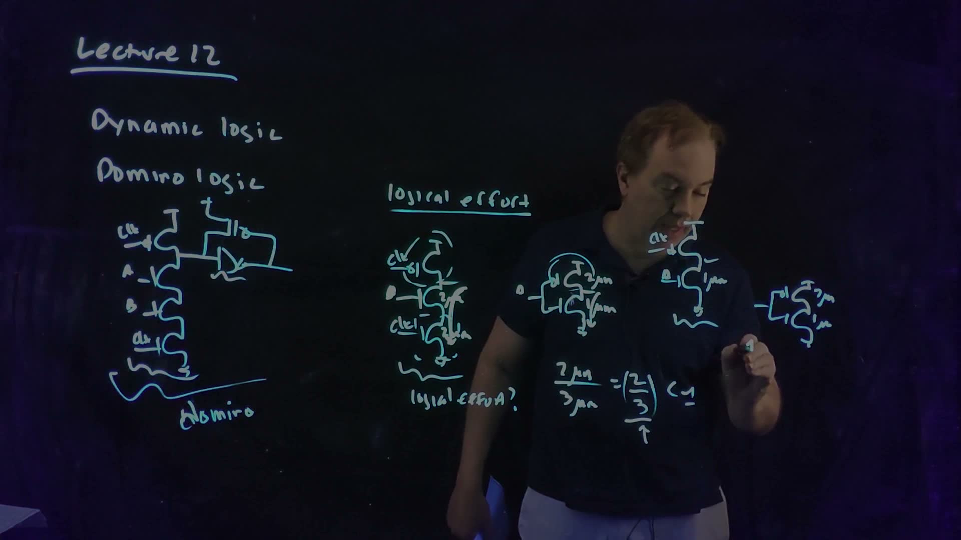
The footed stage
Logical effort of a footed dynamic stage (board, 02:14–03:42)
- The evaluate path is the input B and the footer, in series, each 2 µm board.
- Two 2 µm devices in series pull down like one 1 µm NFET (02:41).
- The balanced inverter with that pull-down is 2 µm/1 µm: its input is (02:47).
- The dynamic stage’s input B is a single 2 µm NFET: 2 µm of gate.
- board: better than an inverter (03:14).
Why (03:14): the input doesn’t “carry along” a PFET. A static gate’s input drives an NFET and a PFET; a dynamic gate’s input drives only the NFET. It wins even though the footer makes it a stack.
The footless stage
“Now imagine I was able to get rid of that evaluate device completely” (03:42) board. The same pull-down now needs only a 1 µm NFET; its inverter is still 2 µm/1 µm, so
That is the whole case for dynamic logic’s speed: no PFETs on the inputs, and, if the footer can go, no stack either. “This also shows you how important it is to get rid of the stack transistor” (04:09). Section 7 shows how.
The general rule
added The two board cases are one rule. Replace the evaluate path (footer included) by the single NFET of the same strength, ; the reference inverter has input ; the input’s own gate width divided by that is .
The precharge PFET does not appear anywhere: it is off during evaluate. If an input drives two devices (it appears twice in the network), its is their sum.
Worked example. added The evaluate delay of Chapter 11’s footed stack (Chapter 11 §4), redone with logical effort: A, B and the footer each 4 µm, 50 fF at (25 µm).
- Three 4 µm devices in series: .
- With the reference inverter’s input is ; input A is 4 µm, so (that is with ).
- ; delay , as Chapter 11 found from .
- At equal strengths the reference is , , delay .
Common mistakes.
- Counting the precharge PFET in or in the reference. The input drives only its NFET; the precharge PFET’s gate is on the clock.
- Leaving the footer out of the stack. It is in the evaluate path: counts it.
- Using the unbalanced reference. The reference is the balanced inverter (2W/W, or W/W at equal strengths) with the stage’s pull-down strength, exactly as for static gates.
Check yourself A footed dynamic NOR4 has four parallel 2 µm input NFETs over one 2 µm footer, Rpfet = 2Rnfet. What is the logical effort of one input? Of a footless version with 1 µm inputs? Compare with the static NOR4 of Chapter 7.
One input’s evaluate path is that input and the footer: two 2 µm devices, , reference , so (the parallel inputs don’t change it). Footless with 1 µm inputs: . The static NOR4 has NFETs and four series PFETs of : , four and a half times the footed dynamic NOR’s. A wide NOR is where dynamic logic gains most.
Check yourself In MT17-3c, a dynamic gate has a 1 µm clocked PFET and three 4 µm NFETs in series (A, B and the clocked footer) driving 50 fF, Cg = 2 fF/µm, and the NFET and PFET have equal strength. Use logical effort to find the delay from A rising, in τinv.
Equal strengths: the reference inverter is W/W. , reference , . . Delay , the same as Chapter 11’s route; the 1 µm PFET plays no part. (This is MT17-3c; its key’s 9.375 τinv is right.)
3. Sizing a domino gate
The idea. Size it like any path: work back from the load with the target gain per stage, on the edges that carry the logic. The inverter’s PFET gets the gain; its NFET is made several times weaker; the dynamic stack is sized to drive the inverter’s input.

The lecture’s example
A domino AND gate: a clock device, inputs A and B, the footer, then the inverter, loaded with 50 fF (05:02–05:16) board. Take (the lecturer notes that the class’s technology is closer to 1, 05:29), so the load is 25 µm of gate. Size each stage for a gain of 3, and only in the direction that carries the logic: the pull-down of the dynamic node, the pull-up of the inverter (05:58). The precharge directions don’t matter.
Sizing the domino AND (board, 05:58–08:51)
- Inverter PFET. For a gain of 3 into 25 µm, the inverter’s normalized inverter has input and NFET ; its PFET is twice that board: (06:26–06:50).
- Inverter NFET. Rule of thumb: the inverter’s PFET at least four times stronger than its NFET (06:58). A PFET has half the strength per micron, so the NFET is times narrower: board (07:21).
- The dynamic stage’s load is the inverter’s input: (07:50).
- Its normalized NFET for a gain of 3: divide by 3, and by 3 again: .
- The stack. A, B and the footer are three in series, so each is three times that board: (08:16).
- The precharge PFET just has to precharge the node in time: “maybe I make this seven tenths micron or something like that” board (08:24). Then check that every stage precharges within the precharge phase.
“And that’s how you size a domino gate using the same kind of tricks that we used for … gain-based sizing for complementary static CMOS” (08:51).
added Unrounded: , , the inverter’s input , and each stack device . The board’s rounded values give 2.1 exactly.
What to notice.
- At the lecture’s settings each stage has gain 3, so the gate takes .
- Remove the footer: the stack drops to two devices, each narrower (1.39 µm), and the input capacitance the gate presents falls with it; the gains stay 3.
- Raise the skew: the inverter’s NFET shrinks, its rising-edge logical effort falls toward 2/3 (its input is nearly all PFET), and the stack can shrink too. The price is the inverter’s switching threshold and noise margin (Chapter 11 §7).
- Switch to equal strengths: the inverter’s PFET halves, and every effort is measured against a W/W inverter.
Common mistakes.
- Sizing the inverter’s NFET for its own gain. It only resets the output during precharge; it is set by the skew, not by the load.
- Forgetting that four times stronger means eight times wider when .
- Sizing the precharge PFET by gain. It has no logic delay; it only has to finish precharging in time.
Check yourself Size a footed two-input domino AND for a 60 fF load with Cg = 2 fF/µm, a gain of 3 per stage, Rpfet = 2Rnfet, and an inverter PFET four times stronger than its NFET. What is the delay in τinv? And the stack widths if the footer is removed (same gains)?
The load is 30 µm. Inverter: normalized NFET , so the PFET is and the NFET ; the inverter’s input is . Dynamic stage: , times 3 for the three-high stack: 2.5 µm each for A, B and the footer. Delay . Footless: a two-high stack, each; its is and , still a gain of 3.
4. What the domino gate gains
The idea. Both stages of the sized gate have logical effort at or below one, so the domino gate needs less path effort than the static gate it replaces. But it is still two stages.
The logical efforts of the result
“This one will be similarly driven down below one because it’s a skewed inverter” (09:02). added The numbers, by the definition of Section 2 applied to each stage’s logical edge:
The efforts of the 50 fF domino AND (added)
- Skewed inverter, rising edge. Its 5.556 µm PFET pulls up like the PFET of a 5.556/2.778 µm balanced inverter, input . Its own input is : . Its ; gain 3.
- Skewed inverter, falling edge (the precharge reset): its 0.694 µm NFET’s balanced inverter has input , so . That edge has time to spare; it is not on the logic path.
- Dynamic stage. A three-high stack: , the inverter’s value. ; gain 3.
- The gate’s path effort is , and .
The lecturer says of the dynamic AND stage that its effort is “greater than one here, but … better than it would for a complementary static CMOS of the same logic function” (09:22). By his own rule it is exactly one for a three-high stack; the comparison holds either way, since the static NAND2 has .
Worked example: against static CMOS. added The static AND is a NAND2 and an inverter. Give it the same input capacitance (2.083 µm per input) and the same 25 µm load, sized for equal gains:
- for both.
- Static: , , two stages of gain 4: .
- Domino: , , two stages of gain 3: . A quarter faster, before counting that the static gate also fights crowbar current.
Skewed gates in general
added The same definition gives any skewed gate’s effort: input capacitance over the balanced inverter that has the same strength on the edge that matters. A static gate after a domino stage, which only ever switches one way during evaluate, can be skewed toward that edge too. Exams that allow it give a limit on the strength ratio (for example “no more than 4 or less than 1/4”).
Check yourself A static NAND2 follows a dynamic stage and only its falling output matters. Its NFETs are W each; its PFETs are skewed to W/4 each (Rpfet = 2Rnfet). What is its logical effort on the falling edge, and on the rising edge? What is its PFET:NFET strength ratio?
Falling: the two NFETs act as ; the balanced inverter with that pull-down has input ; the NAND’s input is , so (the unskewed NAND2’s ). Rising: one PFET alone; its balanced inverter is over , input : . Strength ratio: the PFET’s (NFET-equivalent) over the NFET stack’s is , the limit. (This is the step FN10-9b and FN19-8b need; their key uses 0.833.)
Check yourself A domino path: (I) a dynamic OR with 1 µm inputs over a 1 µm footer drives (II) an inverter with a 4 µm PFET and 1 µm NFET, which drives (III) a dynamic gate of three 1 µm NFETs in series (footer included), which drives (IV) another 4/1 µm inverter loaded by 500 fF. Cg = 2 fF/µm, Rnfet = 4 kΩ·µm, Rpfet = 8 kΩ·µm, so τinv = 24 ps. Estimate the evaluation delay through all four stages.
Logical edges: I and III fall, II and IV rise. (I) , : gain 3.33. (II) the 4 µm PFET matches a 4/2 balanced inverter (input 6 µm), ; it drives III’s 1 µm input, : gain 0.17. (III) , : gain 5. (IV) , : gain 41.7. Sum 50.2 τinv = 1.20 ns. The gains are badly unbalanced: with stage I’s input fixed, and four equal gains of would take about . (This is FN12-8; its key writes the sum as 50.76 and the product as 128.94.)
Still two stages
The domino gate gains on logical effort, “but I still need two stages” (09:33). The inverter is there only because of the race: a dynamic node fed straight into the next dynamic stage starts it discharging before it has decided (10:00, Chapter 11 §5). Is there another way to avoid the race?
5. NP (zipper) domino
The idea. Alternate the polarity. After an n-type stage, whose node rests at 1, put a stage whose evaluating devices are PFETs: a 1 is “off” for a PFET. That p-type stage’s node rests at 0, which is “off” for the NFETs of the next n-type stage. No inverters, no race.
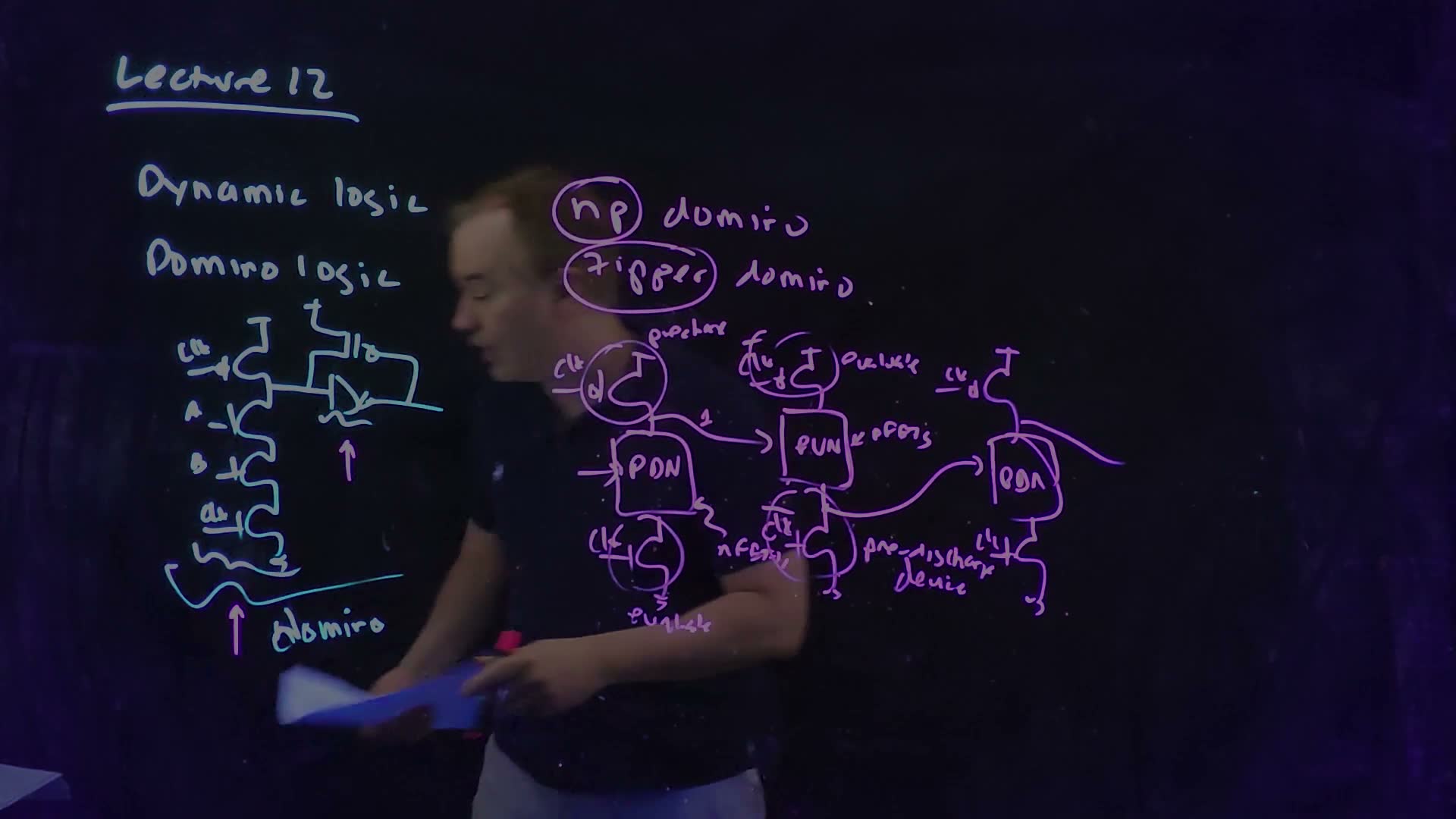
The lecturer only teaches circuit styles that were used in real microprocessors (10:21). This one was: the Digital Equipment Corporation’s Alpha processors of the early 1990s used it widely, in a fully custom design he remembers its engineers presenting “like the tablets coming down from the mountain” (10:47–12:31).
The structure
Start with an ordinary n-type dynamic stage (12:51–13:08) board: the precharge PFET on clk, a pull-down network (PDN) of NFETs, the evaluate (foot) device on clk. Instead of an inverter, its node feeds a second stage built the other way up (13:08–13:58) board:
- a pull-up network (PUN) of PFETs, which does the logic;
- above it, a PFET on : the evaluate device of this stage (on while clk = 1);
- below it, an NFET to ground: the pre-discharge device, on while clk = 0.
While clk = 0, the n stage’s node is precharged to 1 and the p stage’s node is pre-discharged to 0 (13:58). While clk = 1, both evaluate. The p stage’s node feeds another PDN, on clk again, and so on: N, P, N, P, hence “NP domino” (14:25).
(The pre-discharge NFET’s gate is . The lecturer says “clock” for it at 13:37, and its board label is hard to read, but it must be on while clk = 0, “when clock bar is high” as he says at 13:58; on clk it would fight the PUN in every evaluate phase.)
The zipper, and no race
When the dominoes fall, the n node falls down to 0 and the p node falls up to 1: one going down, one going up, “like a zipper opening” (14:43). And there is no race (14:52):
- after precharge the n node is 1, which is off for the PFETs of the p stage it drives, so they can’t turn on falsely;
- the pre-discharged p node is 0, which is off for the NFETs of the next pull-down, so that stage can’t evaluate early either.
Each stage waits for its input to evaluate, as in domino, without the inverters (15:13).
What to notice.
- NP with A = 1: the nodes go 0, 1, 0, 1 in four steps, one stage per step.
- n into n without inverters: every stage after the first is already on after precharge, and the stages that should hold their 1 lose it: the race.
- Domino with inverters: correct, but eight steps for four stages. NP removes those four inverter stages.
The cost
“The negative, of course, here is that my pull-up network is now PFETs” (15:13), and PFETs are worse than NFETs in most technologies. The Alpha designers argued, “quite correctly” in the lecturer’s view, that getting rid of the inverters still brings a delay advantage (15:43). Section 6 puts a number on the cost.
Check yourself In FN12-10b an n-type dynamic stage (precharge PFET and footer on clk) produces Y; Y drives a PFET in a second stage whose top PFET and bottom NFET both take clk, made by an inverter from clk. During which phase of clk does Y evaluate? And Z, the second stage's node?
Both evaluate while clk is high. Y’s stage evaluates with clk = 1 (precharge PFET off, footer on). The second stage is p-type: its header PFET on conducts when = 0, i.e. clk = 1, and its pre-discharge NFET on holds Z at 0 while clk = 0. This is NP domino: Y rests at 1 (off for the PFET it drives) and Z rests at 0. (FN12-10b’s key: both evaluate for clk high.)
Check yourself Why can't a p-type dynamic stage drive another p-type stage directly, any more than an n-type stage can drive an n-type stage?
A pre-discharged p node is 0, and a 0 turns a PFET on. The second p stage would start charging its node before the first had decided: the same race, mirrored. NP domino works because each stage’s resting value is “off” for the devices of the next, which needs the polarity to alternate.
6. Working with p-type stages
The idea. A p-type stage is the mirror of the n-type one. Its node rises when its PFET network conducts, its logical effort uses the PFET-side reference, and the inverter after it (where one is used) is skewed toward its NFET.
Reading the function
added A PFET conducts on a 0: series PFETs conduct when all their gates are 0, parallel ones when any is. The p node rises when the network conducts, so the node equals the network’s conduction function , and an inverter after it gives . (For an n-type stage it is the other way round: node , domino output .)
Check yourself MT24-5a's first stage is p-type: a clocked header PFET above a network of PFETs (A ∥ B) in series with C, all in parallel with A in series with B, and a clocked pre-discharge NFET below; an inverter follows. What does the p node compute, and the inverter?
The network conducts when . That simplifies to : the complement of the majority (the full adder’s carry). The node rises when the network conducts, so the node is and the inverter gives Carry . (This is MT24-5a’s first stage; the key agrees. The exam’s figure gates the pre-discharge NFET with , as it must be; the lecturer says “clock” at 13:37.)
Logical effort of a p-type stage
added Mirror Section 2: replace the evaluate path (header included) by one PFET of the same strength, . The balanced inverter with that pull-up has a PFET and an NFET .
With a p-type stage has twice the logical effort of the n-type stage with the same stack: a two-high p stage has where the n stage has . That factor is the lecturer’s “PFETs are worse” (15:13) as a number. With equal strengths the two are the same.
Check yourself MT24-5 (equal strengths; every device 2 µm). Stage 1 is p-type: input A drives two PFETs, and A's worst evaluate path is three high (header, A, C). Stage 2 is n-type: its input from stage 1's node drives one NFET in a three-high path (that NFET, one of A, B, C, the footer). Find both logical efforts.
Stage 1: ; the W/W reference has input ; A drives : . Stage 2: same path strength, input 2 µm: . (These are MT24-5b’s first two efforts; the key agrees. The midterm kit (M6) takes the delay from there.)
Delays and the inverter after a p node
added A p node rests at 0, rises in evaluate, and is threatened by noise that pulls it up. An inverter after it carries the logic on its falling edge, so it is skewed toward a strong NFET: that lowers its switching threshold and shrinks , the margin that protects the resting 0 (the mirror of Chapter 11 §7). The mirror of the half latch is a weak NFET from the node to ground, driven by the inverter’s output.
Check yourself MT23-3: a p-type stage (clocked PFET M1 above PFETs A ∥ B̄ in series with Ā ∥ B, all 3 µm) drives an inverter with M4 = 10 µm NFET and M3 = 5 µm PFET, loaded by 50 fF. Cg = 1 fF/µm, Rnfet = 1 kΩ·µm, Rpfet = 2 kΩ·µm. With A = 0, find the delay from B falling to Y falling with logical effort.
τinv = 3 × 1 × 1 = 3 ps. Stage 1: B falling turns on the 3 µm PFET B; with A = 0 the charging path is M1, A, B: three 3 µm PFETs, , reference , ; the node drives M3 + M4 = 15 µm, : gain 10. Stage 2: Y falls through M4 (10 µm), whose balanced inverter is 20/10 µm (30 µm): , : gain 1.67. Total , the same as : . (MT23-3b; its key uses , labels ps as ns, and counts one PFET in stage 1 instead of three in series: about 24.2 ps with the 0.69. The inverter’s strong NFET is the skew MT23-3c asks about.)
7. Dropping the footer: delayed-reset clocks
The idea. A footless stage collides only if its precharge starts while its input is still 1. Give it a clock whose falling edge comes a little later, after the stage that drives it has finished its own precharge and its output has fallen to 0.
Why the footer is there, and what it costs
The evaluate device is there to prevent collisions (16:06): entering precharge, the pull-down may still be on, and without a footer current flows straight from to ground. It also costs a device in every stack: Section 2’s against . “The other thing that would really be nice to do here is to get rid of this evaluate device” (16:06).
The collision on one clock
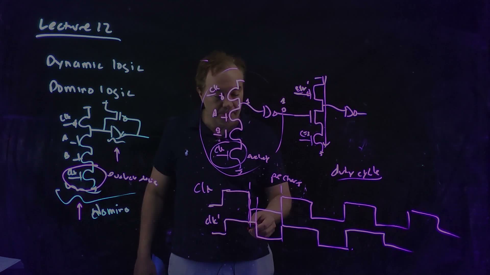
Start with a normal, footed domino stage, and drop the evaluate device from the stage it drives (16:59–17:40) board. Put both on the same clock and follow one precharge (18:10–18:41):
- Suppose stage 1 evaluated: its output is 1, so stage 2’s input NFET is on.
- clk falls. Stage 2’s precharge PFET turns on at once, while its input NFET is still on (nothing has reset stage 1’s output yet): a short-circuit current spike.
- Eventually stage 1 precharges, its output falls, stage 2’s NFET turns off and the spike ends.
“One way to handle this is to say, well, just let it burn” (18:41): the answer is still right in the end. But every stage waits for the one before it to precharge, burning short-circuit power all the while (19:13).
The delayed-reset clock
The better way (19:13) board: drive stage 2 with a different clock, clk′, “whose reset is slightly delayed”. How long a delay? “Long enough to give this first gate time to precharge” (19:48): by the time stage 2 starts precharging, stage 1’s output is already 0, and no short-circuit current can flow.
clk′ rises with clk (evaluation starts together) but falls later, so it is high for more than half the period: its duty cycle, the fraction of the period the clock is high, is above 50% (20:22) board.
Running out of time, and starting again
A third stage, also footless, gets clk″, its reset delayed even more (20:49) board. And so on, but not for ever: each delay comes out of the precharge phase, and “eventually I’m not gonna have enough time to precharge here anymore” (21:04). Then put a footed stage back, on clk again, and repeat (21:20) board. A footed stage cannot collide whatever its inputs are doing: its footer is off whenever its precharge PFET is on. Typically there are about three footless stages between footed ones: footed, footless, footless, footless, footed (21:57–22:05).
Clocks like these are “almost standard fare”: one global clock is distributed over the chip, and local clock generators make the delayed versions (22:05–22:35); clock distribution comes later in the course. Together, they let the designer drop evaluate devices “without paying the penalty of short-circuit current” (22:47).
added A time budget makes “eventually” a number. If the precharge phase lasts , each stage needs to precharge (its node up and its inverter’s output down), and each footless clock falls after the one before, the -th footless stage starts precharging late and needs
What to notice.
- “All on the same clock”: every footless stage collides for , each cycle.
- A delay shorter than shrinks the collision to but doesn’t remove it.
- With and , three footless stages fit and a fourth has no time: the lecture’s “typically three”.
- The duty cycles climb: 50%, 62.5%, 75% with 100 ps steps in an 800 ps period.
Common mistakes.
- Delaying the rising edge too. Evaluation starts together; only the reset (falling) edge moves.
- Applying delayed reset to stages without the domino inverter. It works because stage 1’s output falls to 0 during precharge. A bare dynamic node rises to 1 during precharge, so delaying the next stage’s precharge until then guarantees the collision it was meant to avoid.
Check yourself A domino path has a 500 ps precharge phase. Each stage needs 120 ps to precharge (node up, inverter output down), and each footless stage's clock falls 120 ps after the previous one. How many footless stages can follow a footed one? What goes wrong if the delay is cut to 80 ps?
The -th footless stage needs , so : three (their windows are 380, 260 and 140 ps; a fourth would get 20 ps). With 80 ps each, every footless stage starts precharging 40 ps before its input has finished resetting: a 40 ps collision every cycle in which the stage before it evaluated.
Check yourself A footed dynamic NAND (no inverter after it) drives the NFET of a footless dynamic NOR whose precharge PFET is on its own clock φ′. A designer delays φ′'s falling edge until the NAND has finished precharging, as in delayed reset. Does that prevent collisions in the NOR?
No. The NAND’s precharged output is 1, not 0: once the NAND has precharged, the NOR’s input NFET is certainly on, so the NOR’s precharge PFET turns on into a conducting pull-down. Delayed reset relies on the domino inverter, which makes the upstream output fall to 0 during precharge (18:10). Without it, a footless stage driven by bare dynamic nodes collides whenever any of its inputs is 1 while it precharges. (FN17-2 has this circuit; its key’s answer to 2b applies the delayed-reset rule, and should be re-checked.)
End of the midterm material. “That’s all I wanted to say about dynamic logic” (22:56). The lecture returns to dynamic logic only after latches and clocking, and at 23:15 starts sequential design: latches and flip-flops are after the midterm and not in this guide’s midterm chapters.
Formulas to remember
| Formula | Meaning |
|---|---|
| logical edge: node falls (n), domino output rises | size only for it; the precharge PFET is sized just to precharge in time |
| footed 2 µm + 2 µm: ; footless 1 µm: | the board’s dynamic logical efforts (reference: balanced 2/1 inverter) |
| n-type: (), (equal strengths) | -high evaluate path, footer counted; the precharge PFET never counts |
| p-type: (), (equal strengths) | reference: the balanced inverter with the same PFET; twice the n-type’s |
| inverter PFET ; NFET = PFET/8 for 4:1 strength | domino sizing from the load: 5.6 µm and 0.7 µm for 50 fF, |
| stack device | 2.1 µm each for the three-high AND |
| skewed inverter 8:1 in width: rising, falling | logical effort on each edge |
| domino AND against static (same , 25 µm) | against |
| NP domino: n stage (clk), p stage (header and pre-discharge on ), … | resting 1 is off for PFETs, resting 0 off for NFETs: no race, no inverters |
| p node of its PFET network; n node | which way the node moves when the network conducts |
| delayed reset: clk′ falls after clk; | footless stages without collisions; about three, then a footed stage |
The lecture’s boards