M3. Past midterms: inverters, energy and devices
This page works every past-midterm problem on inverters: the inverter-chain question that every midterm has asked (switching energy, leakage energy, delay and the energy × delay optimum), the noise-margin questions, the single-gate delays in units of , and the device short answers (a forward-biased well, subthreshold current against temperature, FO4 from the transit time). Together they carry 23% to 68% of each past midterm’s points: 23% of MT23, 40% of MT21, 45% of MT24 and 68% of MT17.
Every number below is re-solved here; none is copied from an answer key. Where a key disagrees, the folded note on the key at the end of the part explains why, and the table at the end lists them all.
After this page you can:
- write a chain’s energy per cycle or per transition, its leakage energy, and its delay as functions of and , in the exams’ units;
- find the width that minimizes energy × delay, and say why “minimize the delay” has no finite answer;
- find the PFET/NFET ratio that minimizes a chain’s delay (, or 1 with equal strengths);
- answer the noise-margin questions for noise on every node or on one node, and say how a stronger PFET or a lower gain moves the curve;
- put an inverter’s or a NAND’s delay into units of with equal-strength devices;
- answer the device short answers: FO4 from and , a well tied to the wrong rail, leakage at two temperatures.
Before you start
How to use this page. Each section restates one exam question with its source page (MT23-1b, p3 is Fall 2023, question 1b, physical PDF page 3) and its points, and shows the exam’s own figure. Each family opens with a short How to approach section: how to recognize the question, the moves in order, why the formulas apply, and the traps. Then every part is worked the same way: what it asks, the idea behind the method, the solution in steps (each step gives its reason first), a check on the result, the answer, and one thing to remember. Try each part on your own first; open the Hint if you are stuck, and step through the solution before you press “Show all”. The answer key’s verdict is folded at the end of each part. The chapters teach each method in full, and every solution links the section.
| Family | Questions (most recent first) | Points | Chapters |
|---|---|---|---|
| Inverter chain: energy, leakage, delay, optimum | MT24-2, MT23-1, MT21-4, MT17-4 | 50, 34, 35, 38 | 4, 6, 7 |
| Noise margins and the VTC | MT24-1, MT17-2, MT17-1a (Section 9) | 40, 16, 8 | 6 |
| Single-gate delays in τ_inv | MT17-3a, b, d | 24 | 7, 8 |
| Device short answers | MT21-2, MT17-1b–c (Section 9) | 25, 16 | 4, 5 |
MT17-3c (a dynamic gate’s evaluate delay) is on page M6, with the other dynamic-logic problems.
Conventions the exams use
State these at the top of your answer; the keys mix them, and so do the questions.
- Delay model. A transistor of width driving takes , with in kΩ·µm and in fF; 1 kΩ × 1 fF = 1 ps (Chapter 7, Section 1). No 0.69 factor unless the question asks for one. MT24-2c’s key accepted answers with and without it.
- τ_inv. The FO1 delay of the balanced inverter. With the inverter is 2W/W and ; with equal-strength devices it is W/W and (Chapter 7, Section 7).
- Energy. Each node that rises draws from the supply (Chapter 6, Section 6). “Per transition” (one input edge: only every other node rises) is half of “per cycle” (every node rises once). MT17-4c and MT21-4b ask per transition; MT23-1a and MT24-2a ask per cycle.
- Leakage. Only the device that is off leaks, with the full across it: . Currents are per µm of width (Chapter 4, Section 11).
- Units. fF × V² = fJ. nA × V × ps = J = fJ. Drain capacitance is ignored unless the question includes it.
How to approach an inverter-chain question
Every past midterm has asked this question, for 23–25% of its points. You get a chain of identical inverters, usually with a fixed capacitance on every output (a side load or a wire), driven by a square wave or a single edge. Then the parts build on each other: the switching energy, sometimes the leakage energy and its share of the total, the delay, and a best width (for energy × delay, for delay alone, or the best PFET width). Recognize it by the picture, a chain with a capacitor on every node, and by the phrase “as a function of N and W”.
The moves, in order.
- Find the capacitance on one node first. Every part uses it. A node carries the next inverter’s input, which is both of its gates ( µm of gate), plus the side load. Ignore drain capacitance unless the question includes it.
- Read the device strengths. With equal strengths () the balanced inverter is W/W; with it is 2W/W. In a balanced chain the rising and falling delays are equal, so one stage delay serves both edges.
- Switching energy. Count how many nodes rise in the interval the question names, and charge each one . Per cycle, every node rises once; per transition, half of them do.
- Leakage energy. In each inverter exactly one device is off, with the full across it. Get its current from the subthreshold slope, then multiply by , its width and the time.
- Delay. One stage is ; the chain is stages.
- Optimum. Write the quantity as a function of and find where the part that grows with balances the part that shrinks.
Why these formulas.
- Energy. Raising a node from 0 to pulls the charge out of the supply at the voltage , so the supply delivers . Half is stored on the node and half burns in the PFET. When the node falls, the NFET burns the stored half and the supply delivers nothing (Chapter 6, Section 6).
- Delay. The course models the conducting transistor as a resistor , with in kΩ·µm, that charges or discharges the node; 1 kΩ × 1 fF = 1 ps (Chapter 7, Section 1).
- Leakage. Below threshold the current falls by one decade for every millivolts that the gate is below (Chapter 4, Section 11).
Traps. Per cycle against per transition. (stored) against (drawn). The off device’s width when the inverter isn’t W/W. nA, not pA. Leaving in the answer when the question says it equals the chain’s delay.
1. MT24-2: a W/W chain, energy, leakage and the best width
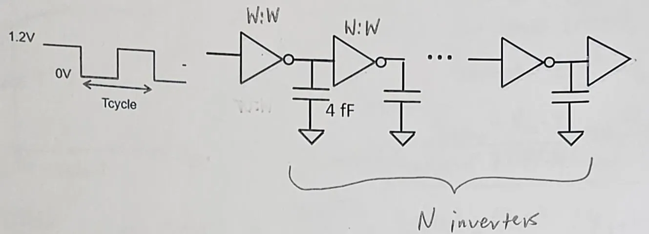
MT24-2, p4 (Fall 2024, 50 points). A chain of W/W inverters (both FETs of width ), each loaded by an additional 4 fF of side-branch loading. , . Ignore drain capacitances. The input is a 50% duty-cycle square wave of period ; .
Before the parts: one node. Every part needs the capacitance on one node of the chain, so find it once. On the output of each inverter hang:
- the next inverter’s input. An input is wired to both gates, the NFET’s () and the PFET’s (), so it presents ;
- the 4 fF side load;
- the inverter’s own drains, which the question tells us to ignore.
The strengths are equal, so a W/W inverter pulls up exactly as hard as it pulls down: every stage has the same delay on both edges. Its fan-out-of-one delay is .
MT24-2a: supply energy per cycle
MT24-2a, p4 (10 points). What is the energy drawn from the supply for this chain of N inverters during ? Express it as a function of N and W. Ignore crowbar currents.
Hint
What it asks. The energy the supply delivers to the whole chain in one full period of the input: one rising edge and one falling edge. The words “during ” decide how many nodes you count. (Questions that say “per transition” mean one edge, and the answer is half as much.)
The idea. The supply delivers energy only when a node is charged up. Raising a node of capacitance from 0 to pulls the charge out of the supply at the voltage , so the supply delivers . Half of it is stored on the node and half burns in the PFET. When the node falls again, the NFET burns the stored half, and the supply delivers nothing (Chapter 6, Section 6). So the energy per cycle is (the number of nodes that rise in one cycle) × . The tempting slip is : that is the energy stored on a node, not the energy drawn from the supply.
Energy per cycle
- Count the rising nodes. An inverter’s output rises when its input falls. On the input’s rising edge nodes 2, 4, 6, … rise; on its falling edge nodes 1, 3, 5, … rise. Over one period, every one of the nodes rises exactly once.
- Price one rise. Each costs , since fF × V² = fJ.
- Add them up. rises: , with in µm.
Check. At each node is 6 fF and costs fJ per cycle, and the formula gives fJ per inverter. ✓ The 5.76 fJ per inverter that doesn’t depend on is the side load’s share (): no choice of removes it.
Answer: .
Remember. Supply energy = (number of rising nodes) × . Per cycle every node rises once; per transition, half of them do.
The answer key agrees
It gives the same expression. A very faint ½ in front of its first line is not carried into its later lines, nor should it be: the ½ is the energy stored, not the energy drawn.
MT24-2b: leakage energy per cycle
MT24-2b, p5 (10 points). What is the total subthreshold leakage energy consumed by these N inverters at 300 K during a cycle? The nFET (pFET) draws at its threshold voltage of 200 mV (−200 mV); the subthreshold slope is 90 mV/decade for both.
Hint
What it asks. Part (a) was the energy spent switching. This part is the energy wasted while nothing switches: current through transistors that are meant to be off. Three things decide it: which transistor is off (and how wide it is), how much current it still passes, and for how long.
The idea. A MOSFET doesn’t shut off at its threshold. Below its current falls exponentially, by one decade (a factor of 10) for every millivolts that the gate is below threshold, where is the subthreshold slope (Chapter 4, Section 11):
(for the PFET, in magnitudes). An “off” transistor has , so its gate sits a full below threshold. That is the only device model this part needs; the rest is bookkeeping.
Leakage energy
- Which device is off, and what is across it? In a settled inverter one device is on and the other off. Output high: the NFET is off, with the output () on its drain and ground on its source. Output low: the PFET is off, with on its source and the output (0 V) on its drain. Either way, each inverter always has exactly one leaking device, with the full across it.
- How far below threshold? and mV (the PFET’s −200 mV in magnitude), so the gate is 200 mV below threshold. At 90 mV per decade that is decades (Chapter 4, Section 11).
- How much current? . (Two decades would divide by 100; a little more than two divides by 167.)
- How wide is the leaking device? Both devices are wide here, so whichever one is off, each inverter leaks nA all the time. (In MT23-1b’s 2W/W inverter the width depends on the output; that is the one new idea there.)
- Energy is power × time. One inverter dissipates , and all do so for the whole cycle: nW.
- Units. nW × s = nJ, so that is nJ with in seconds. With in ps, nW × ps = J = fJ, so it is fJ. Part (c) needs this form.
Check. One 1 µm inverter leaking through a 100 ps cycle: , that is fJ, against the 8.64 fJ it spends switching in (a): about a thousandth. Part (c) makes this comparison exact.
Answer: nJ ( in µm, in s).
Remember. Leakage is always three questions: which device is off and how wide, how many decades below threshold, and for how long. Temperature changes only the slope (MT17-1c, Section 9).
The answer key agrees
It rounds the current to 60 nA/µm.
MT24-2c: the leakage share when the cycle equals the chain delay
MT24-2c, p5 (10 points). Assuming equals the delay of the N-stage chain, what is the ratio of the leakage energy in (b) to the total energy consumed in a cycle, as a function of N and W?
Hint
What it asks. The fraction of all the energy used in one cycle that is leakage, when the clock runs as fast as the chain allows: equals the chain’s delay. “Total” means switching (a) plus leakage (b). Because is now tied to the circuit, it has to be replaced by the delay before you divide.
The idea. The chain’s delay comes from the course’s delay model: the conducting transistor acts as a resistor that charges or discharges the node, so one stage takes (Chapter 7, Section 1), and stages in a row take times as long. Put that into (b), then divide by (a).
Leakage share
- One stage. The driving device is wide with , and it drives : . With equal strengths this holds on both edges (Chapter 7, Section 7).
- The whole chain. .
- Leakage over that cycle. From (b), with in ps: . The in front cancels the of the delay: wider devices leak more, but they shorten the cycle in the same proportion.
- Switching energy, from (a), written the same way: .
- Divide. Leakage ÷ switching . The total is switching plus leakage, so leakage ÷ total .
- Read the result. It doesn’t depend on , and it grows with : a longer chain needs a longer cycle, so each inverter leaks for longer while it still switches only once per cycle.
Check. A second route gives the coefficient directly added. Leakage is for a time , and switching is , so their ratio is : the capacitance and cancel, and a current times a resistance over a voltage has no units, as a ratio must. , and . ✓ For scale: gives a share of , gives 0.50%, and leakage would equal the switching energy only near .
Answer: .
Remember. When is tied to a delay, substitute the delay before you divide. The leakage share is then in disguise: no , and proportional to .
The answer key agrees
It writes , the same expression. With the 0.69 factor in the delay, which the key also accepted, the coefficient becomes .
MT24-2d: the width that minimizes energy × delay
MT24-2d, p6 (10 points). If you can change the sizing of the inverters, what W minimizes the product of the energy in (a) and the delay of the N-stage chain?
Hint
What it asks. The width that makes (the energy per cycle of (a)) × (the chain’s delay) smallest. Why a product: energy alone is smallest for the smallest , and delay alone for the largest (part (e)). The product charges for both, so it has a best width in between.
The idea. Both factors contain . The energy grows with (bigger gates to charge); the delay falls with (stronger devices, so the fixed 4 fF matters less). Their product is smallest where the two effects balance. Find that point by setting the derivative to zero added, or faster: write the product as a sum , which is smallest where its two terms are equal.
Energy × delay
- Multiply. .
- Keep only what depends on W. is a constant factor, so minimize .
- Balance the two terms added. The 4 is constant. As grows, the term grows and shrinks, and their sum is smallest where they are equal: , so . (If were larger than , a smaller would lower the sum, and the other way round.) The derivative agrees: .
- What it means. At each inverter’s own input, , equals the side load. Narrower, and the side load dominates every node, so the delay climbs; wider, and most of the energy goes into driving the inverters’ own gates.
- The numbers there. Each stage takes and the chain ps; the energy is fJ and .
Check. Try the neighbours: is 9 at , 8 at and 9 at . The minimum is at 2, and it is shallow: a width off by a factor of 2 costs only 12.5%.
Answer: , where the gates’ own load equals the 4 fF side load.
Remember. Energy × delay is least where the gates’ own load equals the fixed load. MT23-1d and MT17-4d ask the same thing with other numbers (Section 2, Section 4).
The answer key agrees
MT24-2e: the width that minimizes delay
MT24-2e, p6 (10 points). If the goal is simply to minimize the delay of this chain, what W is required? Think carefully about your answer.
Hint
What it asks. The same chain, but now only the delay counts. “Think carefully” is the exam’s warning that the usual move, setting a derivative to zero, finds nothing here.
The idea. Split one stage’s delay into its two causes: . The first part is the stage driving the next inverter. A wider inverter is stronger by , but its load is larger by too, so this part is the fixed FO1 delay, ps. The second part is the side load, driven by an ever stronger device: it shrinks as and never turns around.
Delay alone
- The chain delay. ps. It falls every time grows: there is no finite minimum.
- The floor. As the side-load part vanishes and each stage becomes a plain FO1: the chain approaches ps but never reaches it.
- Diminishing returns. gives ps, gives ps and gives ps, while the energy per cycle grows in proportion to .
- So the answer is “as wide as possible”, and the careful part is to say why: the side load is fixed, so wider inverters only shrink its share, and the chain can never beat .
Check. The other end: as the delay grows without bound, because ever weaker devices drive a fixed 4 fF. From there the delay only falls toward its floor, so there is nothing in between to minimize.
Answer: (much larger than 2 µm); the delay approaches ps but never reaches it. added Outside this question’s model the first inverter’s input, , also grows, so whatever drives the chain slows down; the question leaves that driver out.
Remember. With a fixed side load and nothing else fixed, minimizing delay has no finite answer. A best width needs a cost on width: the energy, as in (d), or a fixed input capacitance, as in the path-sizing questions (M4).
The answer key agrees
2. MT23-1: the same chain with 2W/W inverters
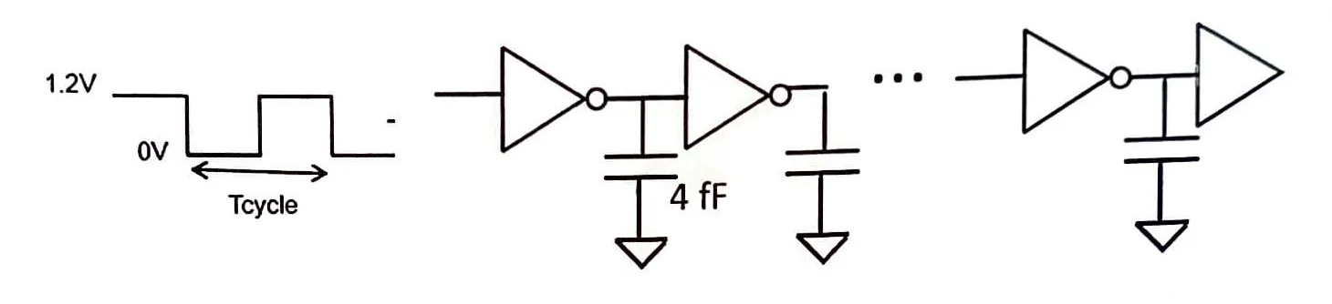
MT23-1, p2 (Fall 2023, 34 points). A chain of 2W/W inverters, each loaded by an additional 4 fF of side-branch loading. , , . Ignore drain capacitances. A 50% duty-cycle square wave of period ; .
Before the parts: what changes from MT24-2. This is the chain of Section 1 a year earlier, and every move is the same. Only the device strengths differ, and three things follow from them.
- The inverter is 2W/W. Here : a PFET passes half the current of an NFET of the same width. To pull up as hard as the NFET pulls down, the PFET is made twice as wide, . Its resistance is then , the same as the NFET’s, so a stage still has one delay for both edges.
- The node is larger. An inverter’s input is wired to both gates, the NFET’s () and the PFET’s (), so it presents . With the 4 fF side load, and drains ignored as the question says,
- The unit of delay is larger. The fan-out-of-one delay is (Chapter 7, Section 7).
The one new idea is in (b): the two devices now have different widths, so the width of the device that leaks depends on whether the output is high or low.
MT23-1a: supply energy per cycle
MT23-1a, p2 (10 points). What is the energy drawn from the supply for this chain during , as a function of N and W? Ignore crowbar currents.
Hint
What it asks. The energy the supply delivers to the whole chain in one full period of the input. “During ” means one rising and one falling input edge, so every node rises once, exactly as in MT24-2a. Only the node’s capacitance has changed.
The idea. Same principle as MT24-2a: the supply delivers energy only when a node is charged. Raising a node of capacitance to draws the charge from the supply at the voltage , so it costs ; a falling node draws nothing (Chapter 6, Section 6). The new part is fF, because the next inverter’s input now has of gate.
Energy per cycle
- Count the rising nodes. An output rises when its input falls, so the odd nodes rise on one input edge and the even nodes on the other. Over one period each of the nodes rises once.
- Price one rise. , since fF × V² = fJ.
- Add them up. , with in µm.
Check. Against MT24-2a’s : the side load’s 5.76 fJ per inverter is the same, and only the term grew, by . That is , the extra gate of the twice-as-wide PFET. ✓
Answer: .
Remember. The energy per cycle is always . The inverter’s sizing enters only through , so count both gates of the next input: for W/W, for 2W/W.
The answer key agrees
MT23-1b: leakage energy per cycle
MT23-1b, p3 (8 points). What is the total subthreshold leakage energy of these N inverters at 300 K during a cycle? at for both devices; 90 mV/decade.
Hint
What it asks. The energy wasted in one cycle by current through the transistors that are off, with the same device numbers as MT24-2b. The difference is that this inverter’s two devices have different widths, so how wide the leaking device is depends on the output’s state.
The idea. Leakage energy is (the off current per µm) (the leaking width) (the time). The current per µm comes from the subthreshold slope, as in MT24-2b: below threshold the current falls one decade for every millivolts that the gate is below , , and an off device has (Chapter 4, Section 11). What is new is the width. With the output high, the NFET () is off; with the output low, the PFET () is. The input is a 50% duty-cycle square wave, so every node spends half of each cycle high and half low, and the leaking width averages .
Leakage energy
- The current per µm. Both devices have mV and 90 mV/decade, so an off gate is decades below threshold, as in MT24-2b: .
- Which device leaks, and when. Because the off device has a different width in each half of the cycle, take the two halves separately. Output high (half the time): the NFET, width , is off, with across it. Output low (the other half): the PFET, width , is off, with across it.
- Average the width over the cycle. Each state lasts half the cycle, so the average off width is .
- Energy is power × time. All inverters leak for the whole cycle: nW.
- Units. nW × s = nJ, so that is nJ with in seconds, or fJ with in ps (nW × ps = fJ). Part (c) needs the second form.
Check. The current per µm is the same as in MT24-2b, because the devices are the same; only the width changed. So the result should be MT24-2b’s times : . ✓
Answer: nJ ( in µm, in s).
Remember. When the inverter isn’t W/W, ask which device is off in each output state, and average their widths over the time the output spends in each state.
The answer key differs
It gives 60 pA/µm and so pJ: a factor 1000 too small. is 60 nA, and the MT24 key, on the same problem, has nA. Its 1.5W counting is right.
MT23-1c: the leakage share
MT23-1c, p3 (8 points). Assuming equals the delay of the N-stage chain, what is the ratio of the leakage energy in (b) to the total energy consumed in a cycle, as a function of N and W?
Hint
What it asks. The fraction of the energy used in one cycle that is leakage, when the cycle is as short as the chain allows. “Total” is switching (a) plus leakage (b). “In a cycle” decides which switching energy to use: (a)‘s, with every node rising once.
The idea. The method is MT24-2c’s: one stage takes in the course’s delay model, where the conducting transistor acts as a resistor (Chapter 7, Section 1); the chain takes stages; put that delay in for in (b), then divide by (a). Two things differ. The stage delay uses . And the leakage share comes out 1.5 times MT24’s, because the leaking width averages while the driving width is still .
Leakage share
- One stage. Falling, the NFET drives the node: ps. Rising, the PFET has kΩ, the same resistance, so the same delay: the 2W/W inverter is balanced.
- The whole chain. ps ps.
- Leakage over that cycle. From (b), with in ps: . The cancels: wider devices leak more, but they shorten the cycle in the same proportion.
- Switching energy, from (a), written the same way: .
- Divide. Leakage ÷ switching . The total is switching plus leakage, so leakage ÷ total .
- Read the result. Again no , and it grows with . For : .
Check. The second route of MT24-2c’s check added gives the coefficient directly. Leakage ÷ switching is (the leaking width ÷ the driving width) × , and MT24-2c found . Here the width ratio is , so . ✓
Answer: , independent of .
Remember. Substitute the delay for before you divide. The share is then (leaking width ÷ driving width) × : no , and proportional to .
The answer key differs
It differs in three ways: it carries the pA slip from (b); it leaves in the answer instead of substituting the chain delay; and it takes the switching energy as fJ, reasoning that in one chain delay “all inverters have switched state once”. That is the energy of one input transition. The question asks for the energy in a cycle, which part (a) found to be twice as much, and the MT24 key uses the full cycle. If your exam asks this, use your part (a) and say so.
MT23-1d: the width that minimizes energy × delay
MT23-1d, p4 (8 points). If you can change the sizing, what W minimizes the product of the energy in (a) and the delay of the chain?
Hint
What it asks. The width that makes (the energy per cycle of (a)) × (the chain’s delay) smallest: MT24-2d with the 2W/W numbers.
The idea. Same balance as MT24-2d. Both factors contain : the energy grows with (more gate to charge), and the delay falls with (stronger devices, so the fixed 4 fF matters less). The product is smallest where the two pulls balance, and that happens where the inverters’ own gate load equals the side load. The only change is that the gate load is now , so the best is smaller than MT24’s 2 µm.
Energy × delay
- Multiply (a) by the chain delay of (c): .
- Keep only what depends on W. is a constant factor, so minimize .
- Balance the two terms added. The 24 is constant; grows and shrinks, and their sum is smallest where they are equal: , so . The derivative agrees: .
- What it means. At the gate load equals the side load, as in MT24-2d.
- The numbers there. Each stage is and the energy is fJ.
Check. Try the neighbours: is 49 at , 48 at and 50 at , so the minimum is at 4/3, and shallow. The energy at the optimum, fJ, is the same as MT24-2d’s, and so is the stage delay in units of : in both exams each node is then twice the side load, 8 fF.
Answer: .
Remember. Energy × delay is least where the gates’ own load equals the fixed load, whatever the inverter’s ratio. Only the gate load per µm changes: for W/W, for 2W/W.
The answer key agrees
Try it
Switch between the two exams’ technologies, move , the side load and , and watch the three curves. The minimum of energy × delay always sits where the inverters’ own gate load equals the side load, and the leakage share never depends on .
What to notice.
- The delay curve flattens toward 1/2 of its value at : the floor of MT24-2e.
- Set the side load to 0: the delay no longer depends on (MT17-4a), and energy × delay is smallest at the smallest .
- Raise : the leakage share grows in proportion; it is the only knob that moves it.
3. MT21-4: four inverters and the best PFET width
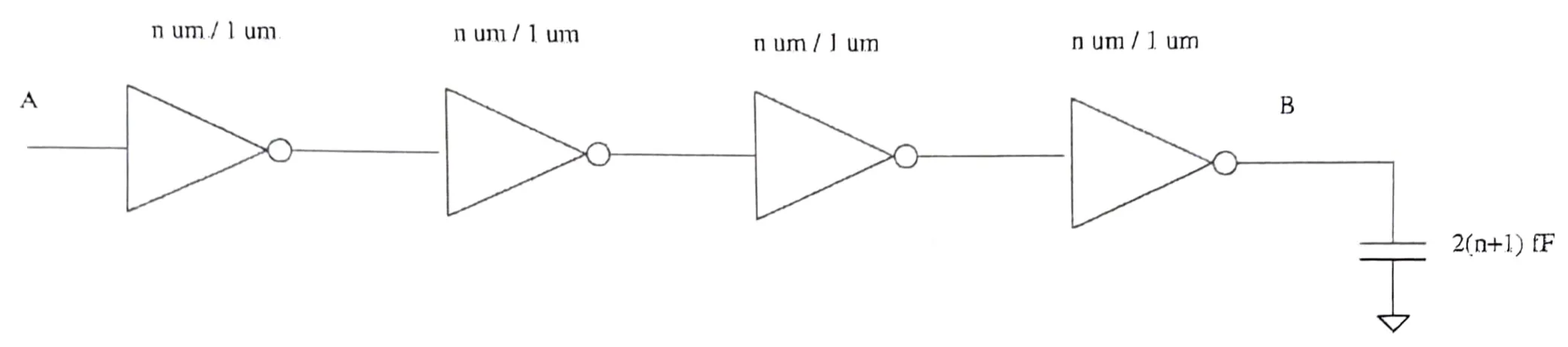
MT21-4, p6 (Fall 2021, 35 points). A chain of four identical inverters sized . They would give equal rise and fall delays if sized 2 µm/1 µm. ; ; . The output B drives fF.
Before the parts: one node. This chain has no side load; what is new is that the PFET’s width is the unknown. Two facts set up every part.
- The strengths. “Equal rise and fall delays if sized 2 µm/1 µm” says that a 2 µm PFET drives as hard as a 1 µm NFET, so . The balanced inverter is the 2/1, and ps is its fan-out-of-one delay.
- Every node is the same. An inner node carries the next inverter’s input, which is wired to both its gates: µm of gate, or fF at 2 fF/µm. The last node, B, has no fifth inverter, but the question loads it with exactly fF, what a fifth inverter would present. So all four inverters drive the same load, a copy of themselves, whatever is. Drains are not counted.
MT21-4a: the delay for n = 2
MT21-4a, p6 (10 points). For , what is the delay from A rising to B rising?
Hint
What it asks. The time for a rising edge at A to come out as a rising edge at B, through four inverters, at . Four inversions take a rise back to a rise; on the way two stages fall and two rise.
The idea. is the fan-out-of-one delay: the balanced inverter driving one copy of itself. In the course’s delay model a stage takes , and for an FO1 the widths cancel: . A wider inverter is stronger by , but its copy is larger by too (Chapter 7, Section 7). At each inverter is the balanced 2/1 and drives its own copy, so every stage is exactly one FO1, on either edge.
- Each stage is an FO1. With each inverter is the balanced 2/1 and drives one copy of itself (the intro’s equal nodes). Because it is balanced, the falling stages (through the NFET) and the rising ones (through the PFET) each take .
- Count the stages. Four of them: .
Check. Price the two kinds of stage separately. A falling stage is the 1 µm NFET driving 3 µm of gate: . A rising stage is the 2 µm PFET, , driving the same 3 µm: also . So two falling and two rising stages give ps. ✓ itself never appears, which is why part (c) can use this result to stand in for it.
Answer: 100 ps.
Remember. A balanced inverter driving its own copy takes whatever its size; a chain of them takes .
The answer key agrees
MT21-4b: energy of one transition
MT21-4b, p7 (10 points). For , what is the energy dissipated by a single transition through this chain? Ignore leakage, crowbar currents and the energy from the source at A; consider only dynamic charging energy.
Hint
What it asks. The energy of one input edge, at . “A single transition” decides the count: A changes once, so only half of the nodes rise (compare MT24-2a, where “during ” made every node rise once). “Dissipated” asks for the heat, not the energy drawn; the two come to the same total here.
The idea. A rising node draws from the supply: half is stored on the node and half burns in the PFET. A falling node draws nothing, and burns its stored in the NFET (Chapter 6, Section 6). In one transition two nodes rise and two fall, so you can count either way.
Energy per transition
- One node. Each carries , and .
- Which nodes rise. A rises, so node 1 falls, node 2 rises, node 3 falls and node 4 (B) rises: two of the four.
- Count the energy drawn. The two rising nodes each draw from the supply: 75 fJ in all.
- Count what is dissipated instead (Chapter 6, Section 6), since that is the question’s word. Each rising node burns half of its 37.5 fJ in its PFET (2 × 18.75 fJ), and each falling node burns its stored 18.75 fJ in its NFET (2 × 18.75 fJ). Total 75 fJ, the same, because as many nodes fall as rise.
Check. The other edge: A falling makes nodes 1 and 3 rise, again two nodes, again 75 fJ. And the key’s form: half of all the capacitance, fJ. ✓
Answer: 75 fJ (for either edge).
Remember. Per transition, half the nodes rise: the energy is , whether you count what is drawn or what is dissipated.
The answer key agrees
It writes it as with fF.
MT21-4c: the PFET width that minimizes the delay
MT21-4c, p7 (15 points). Find the that minimizes the delay from A rising to B rising. Why is it less than two? What would minimize the delay if the nFETs and pFETs had equal strength?
Hint
What it asks. The PFET width (in µm, with the NFET at 1 µm) that makes the A-rising-to-B-rising delay smallest; why that is below 2; and the best if the two devices had equal strength. “From A rising to B rising” fixes which stages fall (1 and 3) and which rise (2 and 4).
The idea. The tempting answer is , the balanced inverter, because it makes the rising and falling delays equal. But equal delays are not the smallest sum. Each stage takes (Chapter 7, Section 1), and appears in both factors: in on every stage, and in the PFET’s resistance on the rising stages only. Write the total as a function of , and find where the part that grows with balances the part that shrinks. isn’t given, so (a)‘s 100 ps has to stand in for it.
Best n
- The falling stages. Every node carries µm of gate. Stages 1 and 3 fall through the 1 µm NFET: each.
- The rising stages. Stages 2 and 4 rise through the µm PFET, whose resistance is : each (Chapter 7, the check on n µm/1 µm).
- Add the four. .
- Calibrate with n = 2. The question gives but not , and part (a) says the chain takes at . Setting in step 3: , so (the 2/1 inverter’s ). The delay is .
- Balance the two terms added, the move first explained in MT24-2d. The 3 is constant; (the PFET’s load on every node) grows and (its resistance on the rising stages) shrinks. Their sum is smallest where they are equal: , so . The derivative agrees: .
- The delay there. , about 3% faster than at .
- Equal strengths. Now the PFET’s resistance is , so the rising term becomes , the total , and (or ) gives .
Check. The sum takes the same value at and at , so gives the same 100 ps as , and the minimum must sit between them at . ✓ The curve is flat there: the best saves only 3%.
Why less than two. The PFET’s width is load on every node, so it slows the falling stages too, but it speeds up only the rising ones. At the two edges are equal; shrinking the PFET a little saves more on the falling stages (lighter load) than it costs on the rising ones. The optimum trades a little rising speed for less load. added In general the best ratio is : here, 1 with equal strengths.
Answer: (97.1 ps instead of 100 ps); with equal strengths.
Remember. Equal rise and fall is not the fastest chain. When the PFET’s width loads the same nodes it drives, the best ratio is . Recognize the question by “find the (or the PFET width) that minimizes the delay”.
The answer key agrees
It drops a factor in its last derivative, which does not change the root.
4. MT17-4: a chain with wiring capacitance
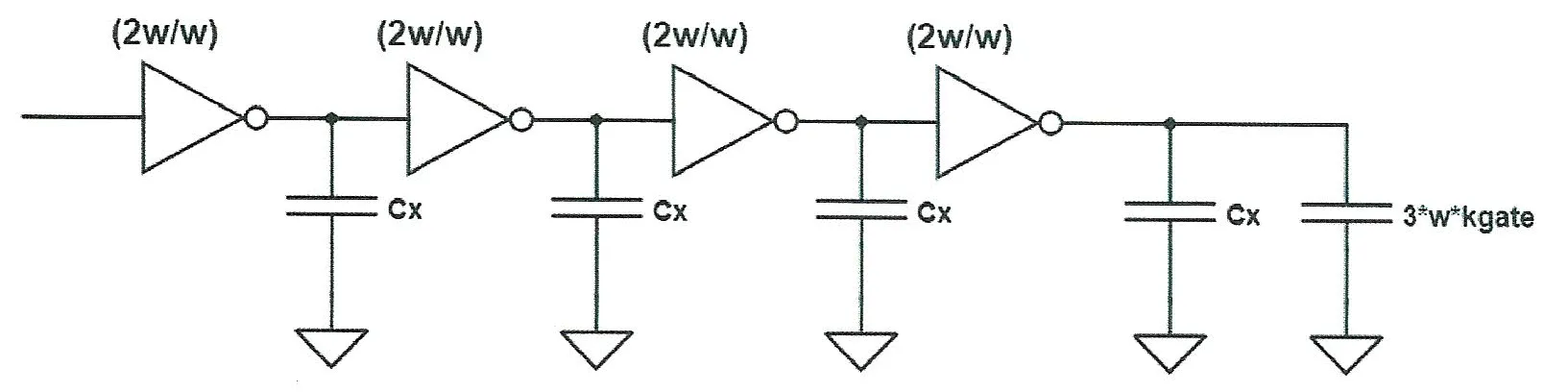
MT17-4, p8 (Fall 2017, 38 points). A chain of four identical inverters sized with an additional wiring capacitance between inverters. They give equal rise and fall delays at . ; ; . The last output carries and .
Before the parts: one node. The same chain again, with two changes: the fixed load is a wire, , given as a symbol instead of a number, and the energy in (c) is per transition. Every part uses the node, so find it once.
- The strengths. Equal rise and fall at means , so the 2W/W inverter is balanced and ps is its fan-out-of-one delay (Chapter 7, Section 7).
- The node. Each output carries the next inverter’s input, both its gates, µm, so ; plus the wire . The last output has no fifth inverter, but the question loads it with , its stand-in. So every node carries .
MT17-4a: no wire
MT17-4a, p8 (8 points). For , what is the delay from A rising to B rising (or falling to falling)? Does it depend on W? Why?
Hint
What it asks. The delay through the four inverters with no wire, and whether the size matters. “Why?” is where the points are: the answer has to name what cancels.
The idea. With , each inverter drives exactly one copy of itself, so each stage is a fan-out-of-one delay, . In the course’s delay model that is : the width appears once in the strength (underneath) and once in the load (on top), and cancels (Chapter 7, Section 7).
- One stage. With no wire the node is , the next inverter’s input. Falling, the NFET drives it: . Rising, the PFET has , the same.
- Four stages: .
- Why W drops out. A wider inverter is stronger by , but its load, the next inverter, is larger by too, and the two cancel. Only a load that doesn’t grow with , such as the wire of (b), makes the size matter.
Check. This is MT21-4a again: four balanced inverters with ps, each driving its own copy, 100 ps. Neither question gives , and neither needs it.
Answer: 100 ps, for any .
Remember. A chain that drives only copies of itself takes , whatever its size. Size helps only against a fixed capacitance.
The answer key agrees
MT17-4b: with the wire
MT17-4b, p8 (10 points). For , what is the delay as a function of W and ? What W minimizes it?
Hint
What it asks. The chain’s delay with the wire, as a formula in and , and the that makes it smallest. It is MT24-2e with a wire in place of the side load, so expect the same “no finite answer”.
The idea. Split one stage: . The first part is (a)‘s , fixed. The second is a fixed wire driven by an ever stronger device: it shrinks as and never turns around. isn’t given, so write it through .
- One stage, with : , since .
- Four stages: with in fF and in µm.
- Which W. Because only the wire term depends on , and it falls every time grows, the delay falls monotonically: it is smallest for , where it approaches 100 ps. For example fF and give 200 ps: the wire equals the gates’ load and doubles the delay.
Check. gives back (a)‘s 100 ps for every . ✓ And as the delay grows without bound, because ever weaker devices drive a fixed wire.
Answer: ; minimized by .
Remember. With a fixed load and nothing else fixed, delay alone wants infinitely wide inverters, and the floor is . A finite best width needs a cost on width, such as the energy in (d).
The answer key agrees
MT17-4c: energy of one transition
MT17-4c, p9 (10 points). What energy is dissipated by a single transition through this chain, as a function of W and ? Ignore leakage, crowbar current and the source at A; consider only dynamic charging energy.
Hint
What it asks. The energy of one input edge, as a formula in and , counting only the charging of the nodes. “A single transition” decides the count, as in MT21-4b: half of the nodes rise.
The idea. A rising node draws from the supply, half stored and half burnt in the PFET; a falling node draws nothing and burns its stored half in the NFET (Chapter 6, Section 6). So count the rising nodes and charge each one , with this question’s node, .
- One node. , from the intro: the next inverter’s input plus the wire.
- Which nodes rise. One input edge makes two nodes rise and two fall: nodes 2 and 4 when A rises, 1 and 3 when it falls.
- Price them. The rising pair draws from the supply; counting dissipation instead gives the same , because as many nodes fall as rise.
- Put in the numbers. With and : fJ.
Check. Units: fF × V² = fJ. ✓ And the trap: per cycle every node would rise once, fJ, twice as much. The question says “a single transition”.
Answer: fJ, with in fF and in µm.
Remember. “Per transition” is one input edge: half of the nodes rise, .
The answer key agrees
It writes J, with the capacitances in farads.
MT17-4d: the width that minimizes energy × delay
MT17-4d, p9 (10 points). Find the W that minimizes the product of the energy in (c) and the delay in (b).
Hint
What it asks. The width that makes (c)‘s energy × (b)‘s delay smallest. The answer is a formula in , because the wire is a symbol.
The idea. The same optimum as MT24-2d. The energy grows with the gate load ; the delay falls with because the fixed wire matters less. Their product is smallest where the gates’ own load equals the fixed load. Two differences change nothing: the fixed load is a wire, and the energy is per transition. Per transition is half of per cycle, a constant factor: it scales the product but doesn’t move its minimum.
- Multiply (c) by (b): .
- Name the gates’ load. Write , the gates’ own load, and drop the constant : minimize .
- Balance the two terms added. grows and shrinks; their sum is smallest where they are equal, , so . The derivative agrees: .
- Back to W. : , so .
- The numbers there. Each node is , so each stage takes , as in MT24-2d: the delay is and the energy .
Check. Put into (b): . ✓ And into (c): . ✓
Answer: , that is .
Remember. The third time the same result: make the gate load equal to the fixed load (MT24-2d, MT23-1d, MT17-4d). At that width every stage takes .
The answer key agrees
How to approach a noise-margin question
Noise-margin questions are explanation questions. They show an inverter’s voltage transfer curve (VTC: the output voltage against the input voltage) and ask how much DC noise a node can take, or which way the curve and the margins move when the inverter changes. They carry real points (MT24-1 was 40 of 200) but almost no arithmetic: the points are for the reasoning.
The one idea behind every part. A gate amplifies noise only where its VTC is steep. Mark the two points where the slope is −1 (Chapter 6, Section 4):
- between them the gain is larger than 1 in size: a disturbance at the input comes out larger at the output, and down a chain it grows until a logic value flips;
- outside them the gain is smaller than 1: a disturbance comes out smaller, and the chain cleans it up.
The upper point is and the lower one . So an input is safely low up to and safely high down to .
The moves.
- Where does the node sit before its noise? That depends on whether the node before it is noisy too: at or if every node is noisy, at the rail if only this one is (MT24-1a and b).
- Where does the next gate start to amplify? At for a low node, at for a high node.
- The margin is the distance between the two. With noise everywhere, and .
- “How does the curve change?” Decide first whether the change moves the curve sideways (the PFET’s strength against the NFET’s) or changes its steepness (the gain). Then say which of the four points move and which way; the margins follow from step 3.
Traps. Pairing with in a margin: they are the same point, but a margin compares one gate’s output with the next gate’s input, so pairs with . Using the switching point (where ) as the limit instead of the −1 points. Giving firm directions for and , which sit on the flat ends and barely move. Thinking that fanout changes a DC margin (MT17-1a).
5. MT24-1: noise on every node or on one node
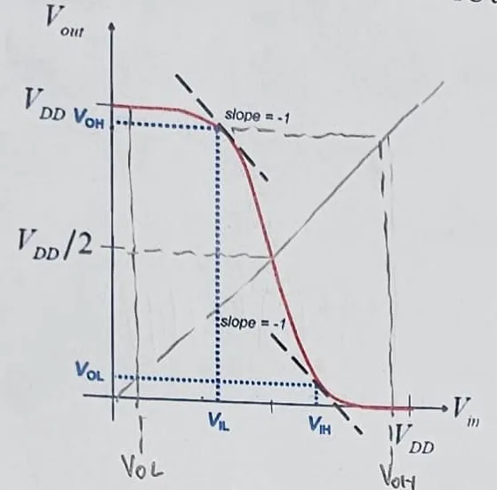

MT24-1, p2 (Fall 2024, 40 points). The VTC of a CMOS inverter, with , , and defined by the points where the slope is −1.
The tools are all in Chapter 6, Sections 4–5. The numbers below come from Chapter 6’s illustrative inverter (5 V, , square law, equal strengths); the exam wants the reasoning, not numbers.
MT24-1a: noise on every node
MT24-1a, p2 (10 points). If DC noise is present on every logic node in the chain, what is the maximum DC noise a low node can tolerate (raising it), and a high node (lowering it)?
Hint
What it asks. A chain of inverters with DC noise on every node, each as large as it can be without breaking the chain. How far can the noise raise a low node, and lower a high node? The words “every logic node” decide the answer: the input of each inverter is itself degraded.
The idea. Picture the lecture’s chain, with a DC noise source between every pair of inverters (Chapter 6, Section 4). With the largest noise everywhere, every inverter is pushed exactly to the edge of amplifying: its input sits at one of the −1 points, and so does its output. The noise on a node may then move it from where its driver leaves it to where the next inverter starts to amplify, and no further.
Noise on every node
- Where a low node starts. Its driver has a high input. With the largest noise, that input has been pulled down from to , the lowest input still read as high, and at the VTC gives the output . So the low node already sits at , not at 0 V.
- Where it must stop. The next inverter starts to amplify when its input rises to . So the noise can add at most .
- A high node, the same way. Its driver’s input has been pushed up to , so it starts at , below . The next inverter amplifies once its input falls to . The noise can take away at most .
- In Chapter 6’s inverter. and : equal, because that inverter is symmetric.
Check. The answer has to hold all along the chain, and it does. A low node pushed up to drives the next inverter to (the upper −1 point), which is exactly where step 3 starts the next, high node; that one, pushed down to , drives the one after it to , where step 1 starts. Every inverter sits at a −1 point, alternating, as the lecture draws it.
Answer: a low node can take (raising it); a high node (lowering it).
Remember. A noise margin is the distance from where the node sits to where the next gate starts to amplify. With noise everywhere, the node starts at or , not at the rail.
The answer key agrees
MT24-1b: noise on one node
MT24-1b, p3 (10 points). If DC noise is present only at a single node, what is the maximum DC noise it can tolerate when low, and when high?
Hint
What it asks. The same two numbers, but now only one node in the chain is noisy.
The idea. The rule of (a) still holds: the margin runs from where the node sits to where the next gate starts to amplify. Only the starting point changes. The driving inverter now has a clean input, at 0 V or , so its output is at the opposite rail: a static CMOS output reaches the rail when its input is clean (Chapter 6, Section 5).
Noise on one node
- A low node starts at 0 V, and the next inverter amplifies at : the noise can raise it by up to .
- A high node starts at , and the next inverter amplifies at : the noise can lower it by up to .
- In Chapter 6’s inverter. 2.046 V for a low node, and for a high one.
Check. Each is larger than in (a) by exactly the head start that the clean driver gives: V on the low side () and V on the high side. That is why the lecture calls the every-node margins “extremely conservative”.
Answer: a low node can take ; a high node .
Remember. Same rule, different starting point: a clean driver leaves the node at the rail, so a single noisy node can take more than the textbook margin.
The answer key agrees
MT24-1c: a stronger PFET
MT24-1c, p3 (10 points). If the pFET is made stronger relative to the nFET, how does the VTC change? What happens to , , , and the values in (a)?
Hint
What it asks. Make the PFET stronger relative to the NFET (wider, for example). How does the VTC change, which way do the four voltages move, and what happens to the two margins of (a)?
The idea. This change moves the curve sideways; it doesn’t change how steep it is. The output switches where the NFET’s pull-down current matches the PFET’s pull-up current. Make the PFET stronger, and the NFET needs a higher input before it can match it: the switching point, and the whole steep part with it, moves right (Chapter 6, Section 4). Read the four points off the moved curve, then apply the margin formulas.
A stronger PFET
- The steep part moves right, and both −1 points move with it: and increase.
- The flat ends barely move. and sit on the nearly flat parts close to the rails, so they change little.
- The margins follow. increases, because its first term rose. decreases, because the term it subtracts rose.
- In Chapter 6’s inverter, with the PFET twice as strong. 2.046 → 2.389 V and 2.954 → 3.282 V, while 4.626 → 4.587 V and 0.374 → 0.294 V. So 1.672 → 2.094 V and 1.672 → 1.305 V.
Check. In words: a strong PFET holds the output high against a rising input for longer, so a low input can take more noise ( up). The same strength makes a high input harder to act on: it has to rise further before the NFET wins ( down). And “barely move” is fair: and move by more than 0.3 V, and by less than 0.1 V.
Answer: the curve shifts right; and rise, and stay about the same; grows and shrinks.
Remember. Changing the strength ratio slides the curve, and trades one margin for the other. MT17-2 asks the same thing with three drawn curves (Section 6).
The answer key agrees
It says that and “stay the same”. That is an approximation: in Chapter 6’s model falls by 0.08 V, small next to the 0.3 V moves of and .
MT24-1d: a lower gain
MT24-1d, p3 (10 points). If the maximum small-signal gain of the inverter decreases with technology scaling, what effect does that have on , , , and the values in (a)?
Hint
What it asks. As technology scales, an inverter’s largest small-signal gain (the steepest slope of its VTC) falls. What happens to the four voltages and to the margins of (a)?
The idea. This change makes the curve less steep instead of moving it sideways. The output still has to fall from near to near 0. With a gentler middle, that fall is spread over a wider range of inputs, so the band where the slope is steeper than −1, between the two −1 points, gets wider on both sides.
A lower gain
- The −1 points spread apart. decreases and increases.
- Both margins shrink. loses through its first term and through its second, as long as and stay put. The band where noise is amplified has grown on both sides.
- In Chapter 6’s inverter. Raising the output slope λ from 0.05 to 0.2 V⁻¹ lowers the peak gain from 30 to 10: 2.046 → 1.885 V, 2.954 → 3.115 V, and both margins 1.672 → 1.521 V.
- and move little, and which way depends on the model. The key’s sketch draws a curve that is shallower everywhere, rounding off sooner at both ends; on that curve falls and rises. In Chapter 6’s square-law model they move by about 0.01 V the other way (4.626 → 4.636 V, 0.374 → 0.364 V).
Check. With the numbers of step 3, the band between the −1 points widens from 0.908 V to 1.230 V, and each margin loses about 0.15 V. The margins’ directions don’t depend on which curve you draw; only those of and do.
Answer: down, up, and both down. For and , give the key’s picture (a curve that sags at both ends: down, up, each worth 2 points in its rubric), and say that it is your sketch’s assumption and that the change is small.
Remember. A sideways move (the strength ratio) trades one margin for the other; a flatter curve (a lower gain) costs both.
The answer key differs
It gives decreasing and increasing as firm directions, worth 2 points each. They depend on how the lower-gain curve is drawn (step 4); the margins’ directions are firm either way.
6. MT17-2: three transfer curves
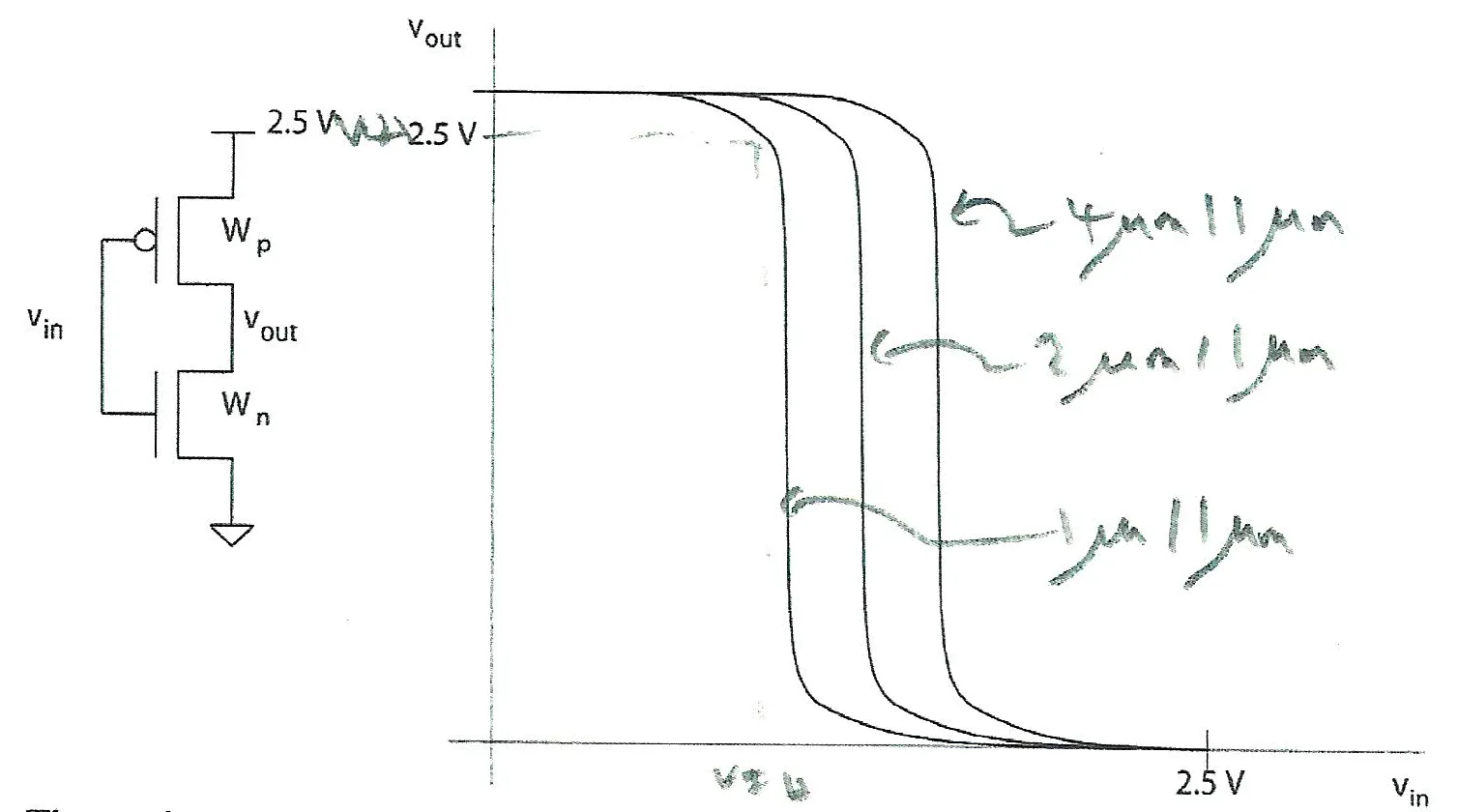
MT17-2, p4 (Fall 2017, 16 points). Three VTCs correspond to = 4 µm/1 µm, 2 µm/1 µm and 1 µm/1 µm. Label the curves and explain. Which gives the largest ? Explain.
Hint
What it asks. Three VTCs, drawn with the same shape but switching at three different inputs, belong to three inverters that differ only in the PFET’s width. Match each curve to its sizing and say why; then say which inverter has the largest , and why. It is MT24-1c with three drawn curves; the moves are in How to approach a noise-margin question.
The idea. Changing changes the strength ratio, and that moves the curve sideways without changing its steepness. The output switches where the NFET’s pull-down current matches the PFET’s pull-up current. A wider PFET pulls up harder, so the NFET needs a higher input before it can match it: the switching point and the whole steep part move right (Chapter 6, Section 4). The margin then follows from where the −1 points sit: , the distance from the high output to the lowest input still read as high.
- Order by strength. The wider the PFET, the stronger its pull-up, and the higher the input must go before the NFET can pull the output down. So the switching point moves right as grows.
- Label the curves. From left to right: 1/1, 2/1, 4/1.
- Read NM_H off each curve. . sits on the flat top, close to 2.5 V on all three curves. , the lower −1 point, moves with the steep part, so it is smallest on the left-most curve.
- Pick the largest. So the 1 µm/1 µm inverter has the largest . It pays with the smallest : a weak PFET lets a low input that is pushed up start pulling the output down sooner (the trade-off of MT24-1c, in reverse).
- Illustration in Chapter 6’s model (5 V; PFET half as strong per µm, so the three are 0.5×, 1× and 2× the NFET’s strength): = 2.094, 1.672 and 1.305 V.
Check. Against MT24-1c: there, doubling the PFET’s strength took from 1.672 to 1.305 V. Here 4/1 is twice as strong as 2/1, and the illustration gives the same two numbers, in the same direction. ✓
Answer: left 1/1, middle 2/1, right 4/1; the largest is the 1/1 inverter’s, because it has the lowest .
Remember. Label VTCs by their switching point: the stronger the PFET, the further right. A weak PFET favours , a strong one .
The answer key agrees
How to approach a gate-delay question
Recognize it by the picture: one gate, an inverter or a NAND, with every transistor labelled with its width, driving a fixed capacitor, and the words “estimate the delays as multiples of the fanout-of-one delay ”. It asks for both edges (input rising to output falling, and the reverse), and, for a stacked gate, how another input’s delay compares. It has appeared once, MT17-3a, b and d, for 24 points. The same conversion is the first move of every path-sizing question (M4’s approach).
The moves, in order.
- Read the strength convention. It sets the unit. Equal strengths: the balanced inverter is W/W and . : it is 2W/W and .
- Convert the load to µm of gate: .
- For each edge, find the conducting path. Output falling: the pull-down NFETs that are on. Output rising: the pull-up PFETs that are on. Then find the path’s effective width .
- Divide. The delay is ; divide it by . With equal strengths that is .
- “How does another input compare?” Argue it from the stack’s internal nodes. The model can’t compute it.
Why these formulas.
- The delay model. The conducting transistor acts as a resistor that charges or discharges the load, so a stage takes (Chapter 7, Section 1).
- The unit. is the balanced inverter driving its own copy. With equal strengths that is : the width cancels (Chapter 7, Section 7). So a delay in units of is the load in µm of gate divided by , the input of a W/W inverter as strong as the path: how many such inverters the load is worth.
- The stack rule. Transistors in series add their resistances, so devices of width in series act as one of width , and in general . Of devices in parallel, only those that are on count; when a single input switches, that is one (Chapter 7, Section 8).
- The bottom of a stack. A device low in a stack must first discharge the internal nodes above it, so it is slower than the model says; the lecture puts the penalty at roughly the square of the stack height (Chapter 8, Section 10).
Decisions to make on the way. Which convention the question states (MT17-3 puts “same strength” in bold italics). Which network carries each edge. Which devices are on for the stated inputs.
Traps. Using when the question says equal strengths. Counting all the parallel PFETs when only one input switches. Forgetting that a stack of acts as of the width. Trying to compute the bottom-input penalty instead of explaining it.
7. MT17-3: gate delays in units of the FO1 delay
MT17-3, p5 (Fall 2017). Estimate the delays as multiples of the fanout-of-one delay . Assume that the nFET and pFET have the same strength. Handwritten on the exam: assume 2 fF/µm of gate capacitance.
Set up once. Every part divides a delay by , so put both in the same terms first.
- The unit. The question says the two devices have the same strength: an NFET and a PFET of the same width drive the same current. So the balanced inverter is W/W, and its fan-out-of-one delay is (Chapter 7, Section 7).
- The load. 50 fF at 2 fF/µm is 25 µm of gate.
- The ratio. A device (or stack) of effective width driving the load takes . Dividing by , the unknown and cancel:
with in µm. In words: the load in µm of gate over , the input of a W/W inverter as strong as the path.
MT17-3a and b: two inverters
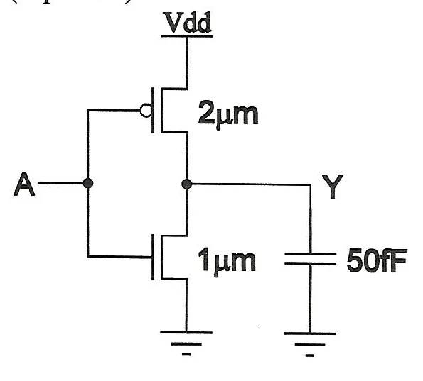
MT17-3a, p5 (8 points). Calculate the A-rising-to-Y-falling and A-falling-to-Y-rising delays of the inverter with a 2 µm PFET and a 1 µm NFET driving 50 fF.
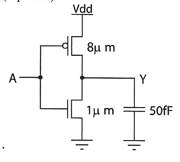
MT17-3b, p5 (8 points). The same with an 8 µm PFET.
Hint
What it asks. For each inverter, two delays in units of : A rising to Y falling, where the NFET discharges the 50 fF, and A falling to Y rising, where the PFET charges it. The two circuits differ only in the PFET’s width, 2 µm in (a) and 8 µm in (b). The bold italics of the question, “the same strength”, decide the unit.
The idea. Each edge has its own conducting path, here a single transistor: the one that is on while the other is off. Its delay is the set-up’s with its width. With equal strengths a PFET counts like an NFET of the same width, so no factor of 2 enters. The tempting slip is the lectures’ default convention, with , as in Chapter 7’s check: the answers would differ. Read which convention the question states.
- Y falling, both circuits. A rises, so the NFET turns on and the PFET off; the 1 µm NFET discharges the load: , in both circuits.
- (a) Y rising. A falls, so the PFET turns on; with equal strengths the 2 µm PFET drives like a 2 µm NFET: .
- (b) Y rising. The same, through the 8 µm PFET: .
- Why (b)‘s falling delay doesn’t change. The PFET is off while Y falls, so its width doesn’t help, and with a fixed 50 fF load it adds nothing to Y. (Its larger gate loads A, which is the previous stage’s concern.)
Check. The rising delay goes as : the 8 µm PFET is 4 times the 2 µm one, and . ✓ Note also that under equal strengths (a)‘s 2/1 inverter is not balanced: it rises twice as fast as it falls.
Answers: (a) 12.5 falling, 6.25 rising; (b) 12.5 falling, 1.56 rising.
Remember. One edge, one conducting path. With equal strengths the delay in is the load in µm of gate divided by twice the path’s width. Read the strength convention before you write .
The answer key differs
It gives 6.75 for (a)‘s rising delay, although its own fraction is : a slip. Its other numbers agree.
MT17-3d: a four-input NAND
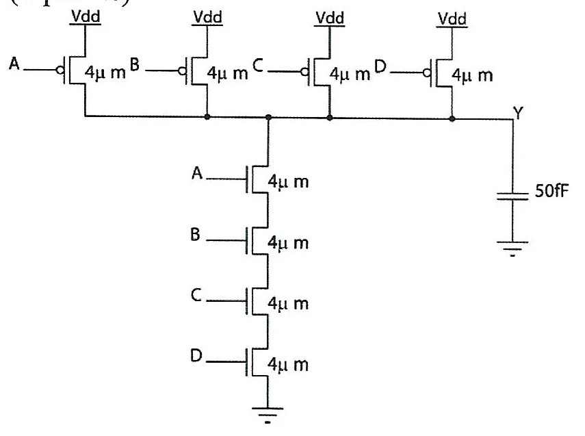
MT17-3d, p7 (8 points). Calculate the delays from A rising to Y falling and A falling to Y rising, with B = C = D = 1. How will the delay from D rising to Y falling (with A = B = C = 1) compare with the A-rising delay? Explain.
Hint
What it asks. The NAND4’s two delays when A switches with B = C = D = 1, in units of , and then a comparison: is D rising (with A = B = C = 1) faster or slower than A rising? “Explain” means the comparison is argued, not computed.
The idea. Two rules from the chapters set the widths. In series, resistances add, so four 4 µm NFETs act like one of µm (Chapter 7, Section 8). In parallel, only the devices that are on count: with B, C and D high, their PFETs are off, and only A’s pulls up. The comparison needs a third idea, the internal nodes between the stacked NFETs (Chapter 8, Section 10). The delay model ignores their capacitance, so it gives every input the same 12.5 ; the difference has to be argued from what those nodes hold before the input switches.
- Y falling: the whole stack. A rises with B, C and D already on, so all four 4 µm NFETs conduct in series. Their resistances add, , so they act like one device a quarter as wide: , and .
- Y rising: one PFET. A falls; B, C and D are high, so their PFETs are off and only A’s 4 µm PFET turns on: .
- What D finds when it rises. Before the edge A, B and C are on and D is off. So the three internal nodes above D are connected through A, B and C to Y, which is high, and they charge to about : an NFET stops passing charge once its gate is only above its source.
- Why that is slower. When D turns on it must discharge those three nodes, as well as Y, through the same stack before Y can fall. More charge through the same current takes longer: D rising is slower.
- Why A is the fast case. When A switches last, B, C and D have been on, so the nodes below A are already at ground and only Y moves. That is the case the model describes, and the lecture says the penalty for a lower input grows about as the square of the stack height.
Check. The stack’s pull-down equals (a)‘s 1 µm NFET, and so does its falling delay, 12.5 : four series devices are sized four times as wide to keep one device’s strength. ✓
Answers: 12.5 falling and 3.125 rising; the D input is slower, because it must first discharge the internal nodes of the stack.
Remember. Series widths combine as ; of parallel devices, only the one that switches counts. The input at the bottom of a stack is the slowest, so a late-arriving signal goes to the input nearest the output.
The answer key agrees
How to approach a device short-answer question
Recognize it by its size: one device or one inverter, few numbers or none, and a request to calculate or explain one thing. The exams’ phrases: “calculate the fanout-of-four delay as a function of the transit time and ”, “is there static DC current? Think carefully about the complete structure of the devices”, “what is at at 300 K? At 400 K?”. MT21-2 carried 25 points and MT17-1b–c 16. (MT17-1a, fanout and the noise margin, belongs to the noise-margin family.)
The moves, in order.
- Name the physics the question tests: a delay (charge over current), a junction (which way it is biased), or subthreshold leakage (decades below threshold).
- Draw what matters. For a delay, the node and every capacitance on it. For a junction, the device’s cross-section: which p and n regions touch, and at what voltages. For leakage, how far the gate is below threshold.
- Write the one relation, with its conditions.
- Put in the numbers or the symbols, keep the units, and say in one sentence what the result means.
Why these formulas.
- Charge over current. A node of capacitance at holds the charge , and a saturated transistor removes it at the current , so the delay is . With a velocity-saturated current and , one device’s is , the transit time (Chapter 5, Section 11).
- Junctions. A MOSFET’s source and drain form p–n junctions with its body. Tying the n well to and the p substrate to ground keeps every one of them reverse-biased; a body tied anywhere else can forward-bias one, and a forward-biased junction conducts heavily (Chapter 5, Section 8).
- Subthreshold current. Below threshold the current falls one decade for every millivolts below , and is proportional to the absolute temperature added (Chapter 4, Section 11).
Decisions to make on the way. The strength convention (a W/W inverter gives a factor 2, a 2W/W one a factor 3). Which rail each body is tied to. What the question holds fixed when the temperature changes (MT17-1c keeps and the current at threshold).
Traps. Taking FO4 as four times FO1: only the gate load grows with the fanout, not the driver’s drains. Reading the transistor symbol instead of the structure. Keeping 60 mV/decade at 400 K.
8. MT21-2: FO4 from the transit time
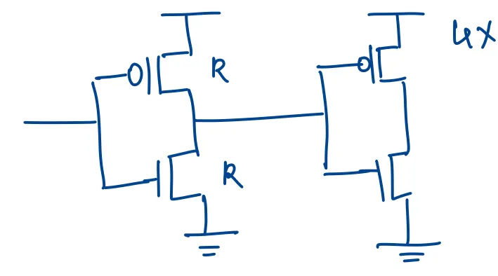
MT21-2, p4 (Fall 2021, 25 points). Calculate the fanout-of-four delay as a function of the transit time and . Assume the pFET has exactly the same drive current as an nFET of the same size.
Hint
What it asks. The fan-out-of-four delay, an inverter driving four copies of itself, as a formula in the transit time and , the ratio of a device’s gate capacitance to its drain capacitance. “Exactly the same drive current as an nFET of the same size” decides the sizing: the inverter is W/W, not the lecture’s 2W/W.
The idea. Delay is charge over current. The output node at holds the charge , and the one transistor that switches removes it at its saturated current , so (Chapter 5, Section 11). For one device with a velocity-saturated current, , and with the ratio becomes : and cancel. So the whole question is to count the capacitance on the node in units of . Count what hangs on the driver’s output node: the input gates of the four loads, and the driver’s own drains, since both of its transistors connect their drains to that node. Each load’s drains sit on the next node, which this delay doesn’t charge, so they are not counted. The tempting slip is FO4 = 4 × FO1, which counts four drivers’ drains.
FO4 of a W/W inverter
- The sizes. Equal currents mean the PFET needs no extra width, so the inverter is W/W: its input is and its own drains are (Chapter 5, Section 12, with a PFET instead of ).
- Charge over current. , and for one device. On either edge one device of width does the work (the NFET falling, the PFET rising, with the same current), so this is the right one.
- FO1 first, as a reference. One load: , using .
- FO4. Four loads’ gates but one driver’s drains: .
Check. Against Chapter 5, Section 13: , the same ratio as for the 2W/W inverter; only the factor 3 becomes 2. For scale: and give FO1 = 7.5 ps and FO4 = 22.5 ps, three times FO1, not four.
Answer: .
Remember. Count the loads’ gates times the fanout, and the driver’s drains once. The strength convention sets the factor: 2 for W/W, 3 for 2W/W.
The answer key agrees
9. MT17-1: short answers (fanout, a grounded well, leakage and temperature)
MT17-1a: fanout and the static noise margin
MT17-1a, p2 (8 points). What effect does fanout have on the static DC noise margin of a CMOS gate? Explain.
Hint
What it asks. Whether driving more gates (a larger fanout) changes a gate’s static DC noise margins, and why. The words “static DC” decide it: the margins belong to the settled, DC behaviour. This is a noise-margin question; its moves are in How to approach a noise-margin question.
The idea. The margins come from the two −1 points of the VTC (Chapter 6, Section 4), and the VTC is the settled output for each input: the output voltage at which the PFET’s current equals the NFET’s. Anything that doesn’t change that balance doesn’t change the margins. A CMOS input is a gate on an oxide, a capacitor, and at DC a capacitor carries no current.
- What sets the margins. The static DC margins come from the DC transfer curve: where the settled output lies for each input (Chapter 6, Section 5).
- What fanout adds. More gates on the output. Each is a capacitor: a CMOS gate input draws no DC current, and a capacitor carries none once it has charged.
- So the balance is unchanged. With no DC current into the loads, the output still settles where the pull-up current equals the pull-down current, for any input. The VTC, , , , and both margins are unchanged.
- What fanout does change. The capacitance to charge, so it only slows the switching.
Check. The limiting case: with a huge fanout the output takes a very long time to settle, but it settles at the same voltage. Speed and level are separate.
Answer: none; the margins are a DC property, and capacitive loading carries no DC current.
Remember. A DC margin comes from the DC curve. A capacitive load changes the timing, never the curve.
The answer key agrees
MT17-1b: a well tied to ground
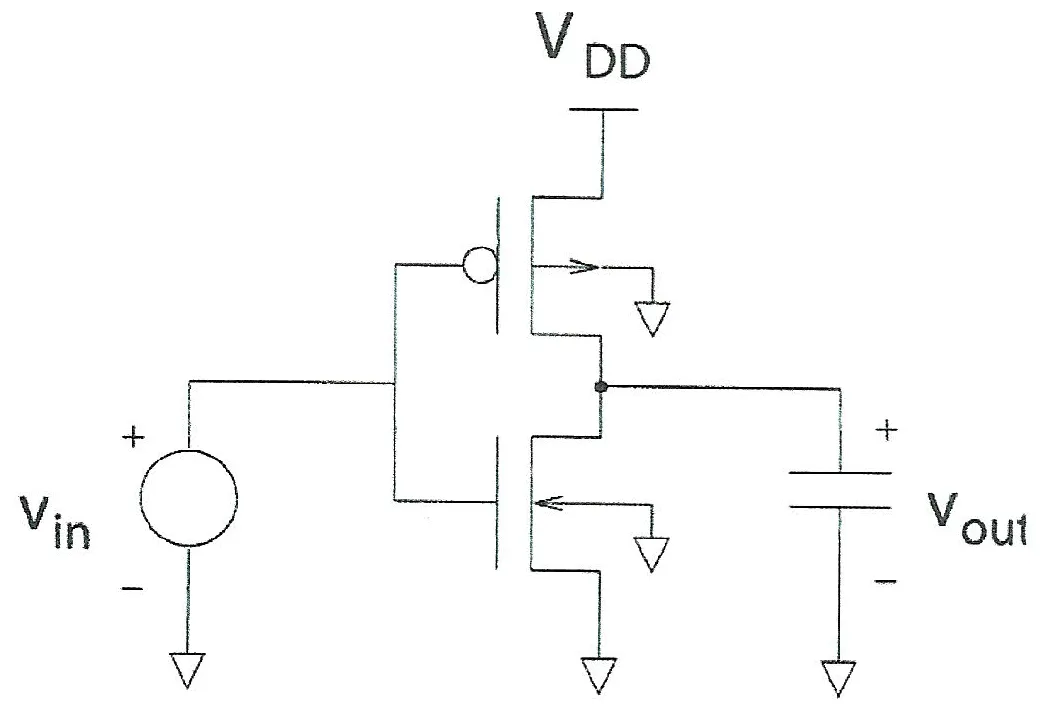
MT17-1b, p2 (8 points). The n well of the pFET is tied to ground. and . Is there static DC current? Explain. Hint: think carefully about the complete structure of the devices.
Hint
What it asks. An inverter whose PFET has its n well (its body) tied to ground instead of , with : does a DC current flow, and why? The exam’s hint, “the complete structure of the devices”, says to look past the transistor symbol to the junctions inside it.
The idea. A MOSFET is also a set of p–n junctions: its source and its drain each form one with the body. The usual ties, the n well to and the p substrate to ground, are chosen so that every one of those junctions stays reverse-biased, whatever the circuit does (Chapter 5, Section 8). Tie a body anywhere else and you have to check each junction. A junction whose p side is well above its n side is forward-biased, and a forward-biased junction conducts heavily. That is the whole argument: the transistor’s on or off state doesn’t enter.
- Look at the structure, not the symbol. The PFET’s source and drain are regions inside the n well, and the well reaches ground through its well contact.
- Bias the source junction. The source is at and the well at 0 V: the p side is 2.5 V above the n side, so that /n junction is forward-biased by 2.5 V.
- Follow the current. A forward-biased junction conducts heavily, so current flows from through the source junction into the well and out of the well contact to ground. It never passes through the channel, so it flows whatever the transistors do.
- The drain as well. With the PFET is on and pulls the output up toward , so the drain junction, in the same grounded well, is forward-biased too.
Check. Put the well back at : the source junction then has 0 V across it and the drain junction is reverse-biased (the output can’t rise above ), so no current flows. Only the tie changed, so the tie causes the current.
Answer: yes, a large static current through the forward-biased source junction (and the drain’s).
Remember. The n well goes to the highest voltage and the p substrate to the lowest. When a question ties a body anywhere else, check every source and drain junction for forward bias. The Fall 2026 instructor calls this kind of circuit “a classic exam problem that I often give” (Fall 2026 Lecture 4, 30:09).
The answer key agrees
It names only the source junction; the drain junction, in the same well, is forward-biased too.
MT17-1c: subthreshold current at two temperatures
MT17-1c, p3 (8 points). If at for an nFET, what is at at 300 K, with a 60 mV/decade subthreshold slope? What is it at 400 K?
Hint
What it asks. The current of an off NFET (, a full volt below its threshold) at 300 K, with a 60 mV/decade slope, and again at 400 K. The words “at 400 K” carry the points: the slope changes with temperature. The problem keeps and the 10 µA at threshold fixed.
The idea. Below threshold the current falls by one decade for every millivolts that the gate is below , , as in MT24-2b (Chapter 4, Section 11). The slope is : carriers cross the barrier by thermal energy, so it is proportional to the absolute temperature added. A hotter device needs more millivolts per decade, so the same 1 V below threshold buys fewer decades of turn-off. Scaling the slope with is the step the exam tests.
- Decades at 300 K. 1000 mV below threshold at 60 mV per decade is decades.
- The current at 300 K. .
- The slope at 400 K. Because is proportional to the absolute temperature added, at 400 K it is .
- Decades and current at 400 K. Now decades: .
- Compare. The leakage grows by : four decades from a third more temperature.
Check. The 300 K slope is the ideal one (, about 60 mV/decade), as it should be at room temperature. And the size of the effect: the number of decades falls by only a quarter (), but the current is an exponential of that number, so a quarter of 16.7 decades is four decades of current.
Answer: A at 300 K and A at 400 K.
Remember. Leakage is counted in decades below threshold, and the slope grows in proportion to the absolute temperature. A modest temperature rise costs orders of magnitude of leakage.
The answer key agrees
Patterns
Inverter chain (every midterm, 23–25% of the points; the approach).
- Moves: the node capacitance first (both gates of the next input plus the fixed load); the strengths; energy = rising nodes × ; leakage = off width × time; delay ; the optimum where the growing and shrinking parts balance.
- Results that come back: energy × delay is least where the gates’ load equals the fixed load; delay alone has no finite optimum; the best PFET ratio is ; cancels from the leakage share.
- Traps: per cycle against per transition; the off width in a 2W/W inverter (1.5W on average); nA, not pA; left in.
- Time: about 15–20 minutes for the full 34–50 points.
Noise margins (MT24-1, MT17-2, MT17-1a; the approach).
- Moves: where the node sits before its noise (/ if every node is noisy, the rail if one is); where the next gate starts to amplify (, ); the margin is the distance; for a change, sideways (strength) or flatter (gain).
- Traps: pairing with in a margin; firm directions for and ; thinking fanout changes a DC margin.
- Time: explanation questions. Two or three sentences and a sketch per part, about 3 minutes each.
Gate delays in τ_inv (MT17-3; the approach).
- Moves: the strength convention ( or ); the load in µm of gate; the conducting path and its effective width for each edge; divide.
- Traps: under equal strengths; all the parallel PFETs counted; a stack of not taken as of the width; computing the bottom-input penalty instead of explaining it.
- Time: one division per delay, a few minutes per part; spend the rest on the stack explanation.
Device short answers (MT21-2, MT17-1b–c; the approach).
- Moves: name the physics; draw the node, the cross-section or the decades; one relation with its conditions.
- Delay is charge over current: loads’ gates times the fanout, the driver’s drains once; factor 2 for W/W, 3 for 2W/W.
- A body tied to the wrong rail forward-biases a junction: large static current. The subthreshold slope scales with the absolute temperature added; count decades.
- Traps: FO4 = 4 × FO1; reading the symbol instead of the structure; 60 mV/decade at 400 K. Time: a few minutes each, most of it on the explanation.
What the keys get wrong
Re-solving every part found these disagreements; all are recorded in this page’s review/decisions.md.
| Part | The key | Here |
|---|---|---|
| MT17-3a | 6.75 rising | |
| MT23-1b | 60 pA/µm, pJ | 60 nA/µm, nJ ( in s) |
| MT23-1c | dynamic energy fJ (one transition), left in, pA carried over | per-cycle energy from (a), = chain delay: |
| MT24-1c | , “stay the same” | about the same (they move by under 0.1 V in Chapter 6’s model) |
| MT24-1d | decreases, increases | depends on how the lower-gain curve is drawn; the margins’ directions are firm |
Every other part (MT17-1a–c, MT17-2, MT17-3b, d, MT17-4a–d, MT21-2, MT21-4a–c, MT23-1a, d, MT24-1a–b, MT24-2a–e) agrees with its key after re-solving.