H1. Homework 1: MOSFET I–V, junction capacitance and scaling
Homework 1 is the course’s own practice for the device chapters: the two I–V models, the pn junction as a capacitor, where a transistor stops conducting, subthreshold leakage, and scaling. This page re-solves every part that the midterm material covers, in the homework’s order, one section per problem.
Every number below is re-solved here and checked in this page’s review/examples.check.ts; none is copied from the key. Where the key disagrees, the folded note on the key at the end of the part explains why, and the table at the end lists them all.
After this page you can:
- read a family of I–V curves and tell square law from velocity saturation by the spacing of the tops, and say how far a device is from the linear limit;
- find the range of a junction capacitance from the range of voltages its node can reach;
- find where a capacitor stops discharging through one or two transistors, and the region of each device on the way;
- count decades of subthreshold current;
- extract and a width from evenly spaced I–V tops, and say why the extracted comes out low;
- scale any quantity when lengths and voltages shrink by different factors.
Before you start
What the source is. The file is the solution key only: the homework’s question text and two of its figures (problems 1b and 4) are not in it. Each part below is restated from what the key shows, its circuits, its given values and its working, and labelled “(from the key)”. Pages are physical PDF pages of the key (HW1-2c, p3). The key gives 20 points to problem 1, 30 to problem 2, 10 to problem 3, 20 to problem 4 and 20 to problem 5.
How to use this page. Every part is worked the same way: what it asks, the idea behind the method, the solution in steps (each step gives its reason first), a check on the result, the answer, and one thing to remember. Try each part on your own first; open the Hint if you are stuck, and step through the solution before you press “Show all”. The answer key’s verdict is folded at the end of each part. The homework’s methods are taught as families on other pages, and each problem links its family’s section: reading an I–V family on page H2, where a transistor stops on page M5, and subthreshold decades on page M3.
| Problem | Parts | Points | Method | Chapters |
|---|---|---|---|---|
| 1 | a: I–V with and without velocity saturation (simulation); b: junction-capacitance range | 20 | the two I–V models; | 3, 4, 5 |
| 2 | a–c: final voltage and regions; d: with a BJT (out) | 30 | regions; a device stops at its own threshold | 4, 10 |
| 3 | subthreshold current at | 10 | count decades | 4 |
| 4 | a: for electrons and holes; b: a width | 20 | 4 | |
| 5 | how ten quantities scale, long-channel and saturated | 20 | constant-field scaling, generalized | 1, 4 |
Conventions.
- PMOS: every NMOS formula holds with for , for and for ; the current flows out of the drain (Chapter 4, Section 9). The key’s plots label the axes and ; for its PMOS they mean and the current out of the drain.
- Problem 2 uses for both device types and a capacitor charged to 5 V (the key’s values). The threshold model: a device conducts while and is off below; subthreshold leakage is ignored there.
- Problem 1b uses the key’s constants: , , .
- Readings from the key’s plot. There is no simulator here. Where a number comes off one of the key’s plots, it says so; the page redoes the arithmetic, it does not reproduce the simulation.
1. HW1-1: PMOS curves and a junction’s capacitance range
HW1-1a: with and without velocity saturation
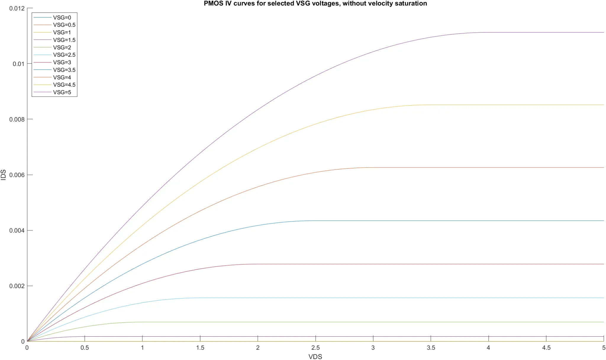
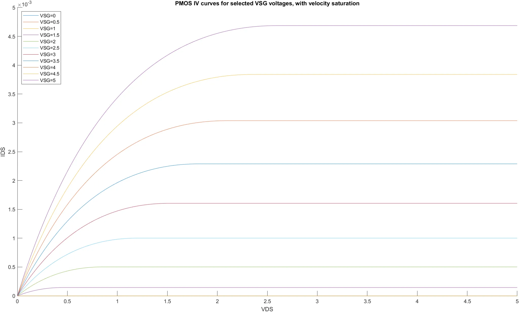
HW1-1a, pp1–2 (10 points; from the key). Plot the PMOS I–V curves for to 5 V in 0.5 V steps, without and with velocity saturation, and explain the difference.
The lecture sets this up: Chapter 4’s velocity-saturated derivation follows Taur and Ning, “and the problem set has you plot the results” (Chapter 4, Section 6, 23:16–23:35). The two plots are the key’s. What follows is how to read them, and a check that they are Chapter 4’s two models.
Hint
What it asks. The key has done the plotting: the same PMOS, first with the long-channel model and then with velocity saturation, for from 0 to 5 V. What is left is “explain the difference”: say what the second family does differently, point to it on the curves, and say why. No device parameters are given, so the explanation has to come from the shapes.
The idea. This is the reading of an I–V family that page H2, Section 2 teaches: look at the spacing of the tops and at where the curves flatten. (H2’s third sign, how the current scales with , needs two channel lengths; here there is one.) What is new is that both families come from one device, so you can measure how far the second one is from each of Chapter 4’s two models.
- Square law (Chapter 4, Section 4): , where is the overdrive and . The curve flattens where the channel pinches off at the drain, at . It holds while the field along the channel stays well below the critical field , so that the carriers drift at .
- Velocity-saturated (Chapter 4, Section 7): the drift velocity levels off near , so more overdrive adds charge to the channel but no more speed. Then with , and the curve flattens earlier, at . Only when is much larger than does approach 1, and the current approach the linear limit .
The quick test between them is to double the overdrive. The square law multiplies the top by 4, the linear limit by 2, and a factor in between means the device is partly saturated. The tempting answer is “with velocity saturation the current is linear”, because the top curves look evenly spaced; the doubling test says how far from linear they really are.
Reading the two families
- Find the threshold first, because both models are written in the overdrive. The , 0.5 and 1 V curves lie on the axis, and 1.5 V is the first that conducts: . Write the overdrive , from 0.5 to 4 V.
- Look where each curve flattens, because the two models put the knee in different places. Without velocity saturation the knee is at : 4 V for the top curve, the long-channel (Chapter 4, Section 4). With it, the top curve flattens near 2.6 V: earlier, as the lecture says (Chapter 4, Section 7).
- Read the tops without velocity saturation, to confirm that the first family is the square law. Readings from the key’s plot (table below): 0.18, 0.70, 1.57, 2.79, … 11.15 mA. Each is with , to within 0.02 mA.
- Read the tops with velocity saturation, the family the question is about. 0.14, 0.50, 1.00, 1.60, … 4.68 mA: lower, and nearly evenly spaced at high overdrive.
- Apply the doubling test, because even spacing alone can’t tell “linear” from “nearly linear”. From to 4 V the long-channel top grows times (square); the velocity-saturated one times. Linear would be 2. So this device is partly velocity-saturated, not fully.
- Fit Chapter 4’s model, to put a number on “partly” added. At the same overdrive, the velocity-saturated current divided by the square law’s is , since . The top curves’ gives and .
- Measure the distance from the linear limit, because “linear” is the claim to test. At , : the current is 35% of , and 42% of the square law’s 11.15 mA.
| (V) | (V) | without: reading (mA) | with: reading (mA) | Chapter 4 model | |
|---|---|---|---|---|---|
| 1.5 | 0.5 | 0.18 | 0.17 | 0.14 | 0.15 |
| 2 | 1 | 0.70 | 0.70 | 0.50 | 0.50 |
| 2.5 | 1.5 | 1.57 | 1.57 | 1.00 | 1.00 |
| 3 | 2 | 2.79 | 2.79 | 1.60 | 1.60 |
| 3.5 | 2.5 | 4.35 | 4.36 | 2.29 | 2.29 |
| 4 | 3 | 6.28 | 6.27 | 3.04 | 3.03 |
| 4.5 | 3.5 | 8.54 | 8.54 | 3.84 | 3.83 |
| 5 | 4 | 11.15 | 11.15 | 4.68 | 4.68 |
The readings are the flat level of each curve, read from the key’s plot images with their axis ticks for scale (about ±0.02 mA). Only the combinations and can be fitted from curves; the device’s own , , and are not in the key.
Check. The fit used only the top curve, so it has to reproduce the others. With and the model gives 0.15, 0.50, 1.60 and 4.68 mA at , 1, 2 and 4 V, within 0.01 mA of every reading (the table’s last column), and at the top: the knee in the plot.
What to notice.
- The dots sit on the lines: the key’s curves are Chapter 4’s models.
- Slide down to about 0.5 V (a channel five times shorter): the doubling ratio falls toward 2 and the curve hugs the linear limit. Slide it up past 20 V: the curve rejoins the square law.
- Even at the plotted the tops look evenly spaced above (steps of 0.69, 0.75, 0.80, 0.84 mA). They still grow; that is the partly saturated regime.
Answer: Velocity saturation lowers the saturated current (to 42% at the top curve) and makes the curves flatten at a smaller (2.6 V instead of 4 V); the tops grow more slowly than the square of the overdrive, tending toward a straight line.
Remember. Double the overdrive and compare the tops: 4 times is the square law, 2 times the linear limit, anything between is partly saturated. Evenly spaced tops at the top of a family don’t yet make it linear.
The answer key differs
Its explanation makes two points. (1), that velocity saturation’s effect grows with the overdrive and lowers the current for a given overdrive, is right. (2) says the saturated current “only goes up linearly with ” with velocity saturation. That is the full-saturation limit of Chapter 4, Section 7, not what its own plot shows: doubling the overdrive from 2 to 4 V gives 2.9 times the current, and the top curve reaches only 35% of the linear limit. Chapter 4 lists this as a common mistake: approaches 1 slowly.
HW1-1b: the junction capacitance of an internal node
HW1-1b, p2 (10 points; from the key). The node C between two series PFETs is a diffusion () of area in an n well () at 5 V, with . Find the range of its junction capacitance.
The homework’s figure for this part is not in the key; the key’s working gives the doping, the area and the node’s range.
Hint
What it asks. Node C is a diffusion inside an n well, so it forms a pn junction with the well, and that junction is a capacitor on the node. Its value is not one number: it depends on the voltage across the junction. “The range” asks for its smallest and largest values over all the voltages the node can reach.
The idea. A reverse-biased junction is a parallel-plate capacitor: its plates are the two edges of the depletion region, with silicon between them, so per area (Chapter 3, Section 5). The depletion width grows with the reverse bias (Chapter 3, Section 3):
Here is the junction’s built-in voltage and its reduced doping (Chapter 3, Section 2). These hold at zero or reverse bias. is always below the lighter doping, and close to it when the other side is much heavier, so the lightly doped side, here the well, sets the width, and most of the depletion region lies in it. A larger reverse bias widens the plates’ spacing and lowers the capacitance. So the question comes down to the node’s voltage range: its two ends give the two ends of the capacitance range.
Capacitance range
- The node’s range, because it sets the reverse bias. C can be charged all the way to 5 V, because a PFET passes a high fully: its source is then the 5 V side, and its doesn’t shrink as C rises. Discharged through the lower PFET, C stops where that PFET turns itself off, one threshold above its gate: with the gate at 0 V (the key’s range implies it; the figure is missing), at (Chapter 10, Section 5; problem 2 works this out). So C lies between 1 V and 5 V.
- The reverse bias, because the voltage across the junction, not the node’s own voltage, sets the width. The node sits in an n well at 5 V, so : from 0 V (node at 5 V) to 4 V (node at 1 V). The node never rises above the well, so the junction is never forward-biased and the formulas hold over the whole range (Chapter 5, Section 8).
- Reduced doping and built-in voltage, the two junction numbers the width needs (Chapter 3, Sections 2–3): , and .
- Zero bias first, because the narrowest depletion region gives the largest capacitance (Chapter 3, Section 3): , 93% of it in the lighter well.
- The largest capacitance, because a parallel-plate capacitor per area is the permittivity divided by the plate spacing, and the spacing here is the depletion width: (Chapter 3, Section 5). Times : .
- Full reverse bias, , because the widest region gives the smallest capacitance. The width grows as : , , .
Check. The ratio of the two ends needs none of the constants. goes as , and as , so . The two values give , the same to rounding. ✓
Answer: from 10.6 fF (node at 1 V) to 25.0 fF (node at 5 V). The capacitance falls as the node falls, because the reverse bias grows (Chapter 5, Section 5: the nonlinear capacitance the lecture warns about).
Remember. A junction capacitance is a range, not a value. Turn the node’s voltage range into a reverse-bias range against its well or substrate, and evaluate at both ends: largest at the smallest reverse bias.
The answer key differs
It gives and . It rounds the widths to two digits before dividing (120 nm for 124 nm, 290 nm for 292 nm), which puts 3.7% high. Its method and its range of bias are right.
2. HW1-2: a capacitor discharged through transistors
HW1-2, pp3–4 (30 points; from the key). A capacitor charged to 5 V discharges through the circuits below (). For each, find the capacitor’s final voltage and the region each transistor passes through. For (c), the capacitance of node is much smaller than the load capacitor.
The rule for all three. This is the threshold rule of page M5’s pass-transistor section, applied to a capacitor instead of a logic node. What this problem adds is the region of each device along the way. Three moves, each for a reason:
- Find each transistor’s source, the terminal nearer its own rail: the lower one for an NFET, the higher one for a PFET. A MOSFET is symmetric, so the voltages, not the drawing, decide which terminal is the source, and (or ) is measured from it.
- Ask when (or ) falls to the threshold, because in the threshold model a device conducts only while . When the source is the node that moves, the moving node changes itself: the device turns itself off at its threshold, and the node stops there (Chapter 10, Section 5). A source on a rail never moves, so then never changes.
- Name the region from , because the question asks for it. A conducting device is saturated while , because the channel is then pinched off at its drain end, and in triode below that (Chapter 4, Section 4). For a PFET read , and .
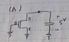
HW1-2a: an NFET with its gate grounded
Hint
What it asks. An NFET with its gate and source grounded and its drain on the capacitor’s charged top. Does the capacitor discharge through it, and how far?
The idea. Whether an NFET conducts depends on alone, not on its drain. Its source is its lower terminal, here the grounded one, and its gate is grounded too, so . The capacitor sits on the drain, so nothing it does can move : the rule’s second move answers the question at once.
- Find the source, because is measured from it. The NFET’s terminals are at 0 V and 5 V; the lower one, ground, is the source. Its gate is at 0 V: .
- Ask whether can change, because a discharging node would move a source that sat on it. The source is on the ground rail and the capacitor is on the drain, so nothing the capacitor does changes . The device never turns on, and with no current the capacitor keeps its charge.
Check. The opposite case shows the gate is what holds the charge. With the gate at 5 V, would be 5 V, the source would still be at ground, and the NFET would stay on until the capacitor reached 0 V: an NFET passes a 0 fully. With its gate at 0 V it passes nothing.
Answer: ; the NFET is in cut-off throughout. In the threshold model the capacitor holds; really, subthreshold leakage (Chapter 4, Section 11) would bleed it slowly added.
Remember. Ask first whether the moving node is the source. If the source sits on a rail, is fixed, and the device is on or off for good.
The answer key agrees
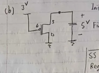
HW1-2b: a PFET with its gate at 3 V
Hint
What it asks. A PFET with its gate held at 3 V, between the charged capacitor and ground. How far does the capacitor discharge, and in which regions is the PFET on the way?
The idea. Now the moving node is the source. A PFET’s source is its higher terminal, the capacitor, so falls as the capacitor discharges. The PFET turns itself off when reaches , at : M5’s rule that a PFET passes a low only down to one threshold above its gate. For the region, compare with the overdrive .
- Find the source and the drain, because both voltages are measured from the source. The higher terminal, the capacitor, is the source: . Its drain is at ground, so .
- The start, because the region is decided at each moment, beginning with the first. : on, with 1 V of overdrive. : saturation.
- On the way down, because and the overdrive both fall as the capacitor discharges. stays above the overdrive , so the device stays saturated all the way.
- Where it stops, because the falling source is turning the device off. It stops when : , so . There it is in cut-off.
Check. At every moment exceeds the overdrive by , so step 3 holds with room to spare: with its drain at ground and its gate above ground, this PFET is saturated whenever it conducts. And the end point is one threshold above the gate, , as the rule says.
Answer: (gate voltage plus ); saturation, then cut-off.
Remember. A PFET that discharges a node stops it at , one threshold above its gate, never at ground. Chapter 10 has a check on the same structure with other numbers (Section 5).
The answer key agrees
HW1-2c: two PFETs in series
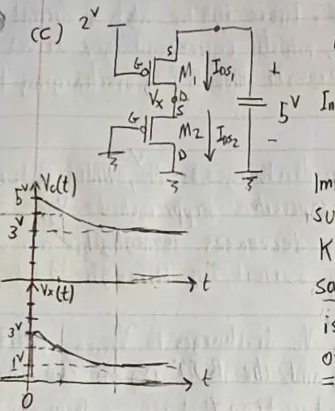
Hint
What it asks. Two PFETs in series between the capacitor and ground: M1’s gate at 2 V, M2’s at 0 V, and a small node between them. Where do the capacitor and end, and through which regions does each device pass? “Much smaller than the load capacitor” decides how behaves: it settles almost at once, while the capacitor discharges slowly.
The idea. The rule gives the end points; Kirchhoff’s current law gives the path.
- The end points. Each device stops at its own threshold, measured from its own source and its own gate: M1 when , M2 when . A series pair does not lose a threshold per device.
- The path. The regions need , and comes from KCL. A node with almost no capacitance can’t store charge, so the current in through M1 must equal the current out through M2. With both saturated and equal (the key’s implicit assumption), equal currents mean equal , because a saturated device’s current depends only on its overdrive (Chapter 4, Section 4).
Two PFETs in series
- Where each stops, because that needs only the gates and the thresholds. M1’s source is the capacitor: it conducts while , so the capacitor can fall only to . M2’s source is : it conducts while , so can fall only to 1 V. Each device stops at its own threshold.
- The start, because the regions are read from the voltages at each moment. The key assumes . Then M1 has and : saturated. M2 has : off.
- charges at once, because M1’s current has nowhere to go but the small node capacitance at . So rises almost instantly, until M2 carries the same current (KCL).
- Equal currents, to find where settles. With equal devices (the key’s implicit assumption) and both saturated, equal currents need equal : , so . Then M1 has , exactly its overdrive: on the edge of saturation. M2 has against 2 V of overdrive: saturated.
- The discharge, because the regions must still hold as both voltages fall. As falls, follows, by the equal- condition of step 4. M1: . M2: . Both stay saturated.
- The end, because the equal- condition brings both devices to their thresholds at the same moment. Both stop together: , , both in cut-off.
Check. Two routes agree. Step 1 found the end points from the gate voltages alone, with no currents; steps 3–6 followed the currents and ended at the same 3 V and 1 V. They must agree, because the KCL path can only stop where some device has reached its threshold.
Answer: and . M1: saturation, the triode/saturation edge, saturation, cut-off. M2: cut-off, saturation, cut-off.
The final voltages don’t depend on the sizes; the path does. added If M2 were weaker than M1, the equal-current would sit higher, above 3 V at the start, and M1 would begin in triode. The end points, 3 V and 1 V, are set by the gate voltages and the thresholds alone. That is the habit the midterms test: “where does it stop?” needs only (M5, MT21-1b asks it of an NFET passing a 1).
Remember. In a series chain each device stops at its own threshold, from its own gate. The regions on the way need one more tool: KCL at the node between the devices.
Check yourself In circuit (c), M1's gate is moved from 2 V to 0 V. Where do VC and VX end?
M1 now conducts while , so the capacitor falls to 1 V; M2 stops at 1 V. Both end at 1 V: a PFET with its gate at 0 V passes a low only down to , and a second one in series, also with its gate at 0 V, adds no further drop (one threshold, not two).
The answer key agrees
Its waveforms show the same path: falls from 5 V to 3 V, while jumps to 3 V and decays to 1 V. It takes M1 and M2 to be equal without saying so (step 4).
HW1-2d: the same with a bipolar transistor
HW1-2d (p4) discharges the capacitor through an NFET whose source drives the base of an NPN transistor. It is out of scope: no lecture before the midterm cutoff teaches a BJT’s regions or its ; Lecture 3 only contrasts the bipolar device with the MOSFET’s symmetry (Chapter 3, Section 6).
3. HW1-3: subthreshold current at zero gate voltage
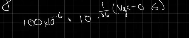
HW1-3, p5 (10 points; from the key). A transistor carries at , with a 60 mV/decade subthreshold slope. Find at .
Hint
What it asks. The current of the transistor when it is off, at , given its current at threshold (100 µA at 0.5 V) and its subthreshold slope (60 mV per decade). Nothing else about the device is needed.
The idea. This is the decade count of page M3’s device short-answer section, in its plainest form: one device at one temperature. A MOSFET doesn’t shut off at its threshold. Below its current falls by one decade, a factor of 10, for every millivolts that the gate is below threshold (Chapter 4, Section 11):
is the subthreshold slope, here 60 mV/decade. The current at threshold multiplies the exponential: each decade divides it by 10. So the whole answer is a count of decades.
- Write the law, because the question gives exactly its inputs, the current at threshold and the slope (Chapter 4, Section 11): .
- Count the decades, because each one divides the current by 10. From 0.5 V down to 0: decades.
- Turn them into a factor, because the law needs the factor by which the current falls, not the count: .
- Multiply the current at threshold, since the law is a product: .
Check. The size, from the count alone: 8.33 decades lies between 8 and 9, so the current must lie between and . ✓ And the slope is a sensible one: 60 mV/decade is the ideal room-temperature slope, .
Answer: .
Remember. The off current is the current at threshold, divided by 10 once for every millivolts below threshold. It is the same move as M3’s MT17-1c (16.7 decades at 300 K, 12.5 at 400 K) and the leakage step of MT24-2b and MT23-1b (2.22 decades: about 60 nA/µm).
The answer key agrees
Its boxed answer is 0.46 pA. Its written expression joins and with what reads as a “+”; it must be a product (a sum would give 100 µA at ), and the boxed 0.46 pA is the product.
4. HW1-4: saturation velocity and width from I–V curves
HW1-4, p5 (20 points; from the key). Figures 1 (NMOS) and 2 (PMOS) show I–V curves of devices wide with . (a) Are they velocity-saturated? Find the saturation velocity of electrons and of holes. (b) Find the width of an NMOS whose saturated current steps by 1.8 mA for each 0.5 V of .
The two figures are not in the key; its working gives the readings: the NMOS tops step by about 160 µA (its prose says 170 µA) and the PMOS tops by about 80 µA, per 0.5 V of gate voltage. Part (b)‘s wording is reconstructed from the key’s calculation.
HW1-4a: the saturation velocity of electrons and holes
Hint
What it asks. Two families of curves, NMOS and PMOS, both 1 µm wide with a 5.8 nm oxide. Decide whether they are velocity-saturated, then extract for electrons (the NMOS) and for holes (the PMOS). Only the oxide and the width are given: no , no , no mobility. That decides the method: it can use only the spacing of the tops.
The idea. This is the spacing sign of page H2, Section 2; what is new is turning the spacing into a velocity. Evenly spaced tops mean the saturated current is linear in the overdrive: the fully velocity-saturated limit of Chapter 4, Section 7,
which holds when , in short channels. It is the channel’s charge per area, , times the width, moving at . Take the difference between two tops: cancels and leaves , in which every factor is known except . (The square law would give steps that grow: starting at threshold, equal steps of give currents in the ratio 1 : 4 : 9 : 16, so steps in the ratio 1 : 3 : 5 : 7.)
- Decide the model first, because the formula depends on it. The key reads the tops as evenly spaced: current linear in the overdrive, not its square. That is the signature of velocity saturation (Chapter 4, Section 7).
- Take the difference of two tops, because is not given and the difference removes it. In the limit, , so a step of adds , whatever is.
- The oxide capacitance, the one factor still to compute: .
- Electrons, from the NMOS steps (160 µA per 0.5 V, a reading from the key’s figures): (with 170 µA, ).
- Holes, from the PMOS steps (80 µA), with the same denominator: , half the electrons’ value.
Check. The units: , and a farad times a volt is a coulomb, an ampere a coulomb per second, so the result is in cm/s. ✓ And the ratio: the two devices share , and , so half the current per step must mean half the velocity.
Answer: for electrons and for holes (readings from the key’s figures).
Why these come out below silicon’s . added The method assumes the full limit. A partly saturated device’s tops grow by less than per step, so the fit returns a smaller, effective . HW1-1a shows it: its top step, 3.5 to 4 V, is about 1.7 mA/V, only half of that device’s limit slope . Read an extracted as a lower bound.
Remember. With evenly spaced tops, divide the current step by and you have , without knowing . Unless the device is fully saturated, the result is a lower bound.
The answer key agrees
Its prose says 170 µA, but its arithmetic and its boxed answer use 160 µA (170 µA would give ).
HW1-4b: the width
Hint
What it asks. An NMOS on the same process whose tops step by 1.8 mA per 0.5 V, instead of (a)‘s 160 µA. How wide is it?
The idea. The step formula of (a), solved for the width: . The same oxide and the same carriers (electrons) give the same and as in (a). In the velocity-saturated limit the current is proportional to the width and doesn’t depend on (Chapter 4, Section 7), so the width is the only thing that can make the step larger.
- Solve the step formula for W, because the oxide, the carriers and are all as in (a): .
- Put in (a)‘s values, with its rounded : .
Check. A second route needs no constants. The current per step scales with , so , the same to the rounding of (10.6 µm with the 170 µA reading).
Answer: .
Remember. In the velocity-saturated limit the current per volt of overdrive is proportional to the width alone, so a width is a ratio of current steps times a known width.
The answer key differs
It writes "". The quotient is cm; rounding it to one digit makes the width 11% small.
5. HW1-5: scaling with a field factor
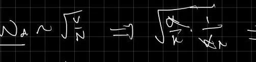
HW1-5, pp6–7 (20 points; from the key). Dimensions scale by , voltages by and doping by , so fields grow by . How do the depletion width, capacitance, inversion charge, drift velocity, current, delay, power, power-delay product, circuit density and power density scale, for a long-channel and for a velocity-saturated device?
Hint
What it asks. A scaling rule that is not Chapter 4’s: lengths shrink by but voltages only by , so every field grows by , and the doping rises by . Find how ten quantities scale, twice: for a long-channel device and for a velocity-saturated one. The second column is the point of the problem, because the two devices’ carriers respond differently to a larger field.
The idea. Chapter 4, Section 10 does this for constant-field scaling, . The homework lets the field grow by added: voltages fall more slowly than lengths, as they did in practice once stopped scaling (Section 11). The method is the lecture’s: write each quantity as a product of quantities already scaled, in order, so that every line uses only the lines above it. The relations are Chapter 4’s:
- the depletion width, (Chapter 3’s formula; the homework assumes that scales with the other voltages, which Section 11 says it doesn’t in practice);
- a device’s capacitance, : its area times ;
- the inversion charge per area, ;
- the current, : charge per area, times width, times drift velocity;
- the delay, : the time the current takes to move the charge ;
- the power, .
Only the drift velocity differs between the two devices. In a long channel grows with the field; a velocity-saturated carrier already moves at , which doesn’t scale.
Quantity by quantity
- Depletion width first, because it needs only a voltage and a doping: . The extra doping exactly offsets the extra voltage.
- Capacitance, because it needs only lengths: .
- Inversion charge per area, because the current is built on it: . The voltage falls more slowly than the oxide thins, so each area of channel holds more charge.
- Drift velocity, the one line where the devices differ: long-channel ; velocity-saturated (it doesn’t scale).
- Current, charge per area times width times velocity, : long-channel ; saturated .
- Delay, the time to move the charge at the current : long-channel ; saturated .
- Power , current times voltage: long-channel ; saturated .
- Power × delay, from lines 6 and 7: long-channel ; saturated . The same.
- Circuit density , because each device’s area shrinks as : for both. Power density , the power per device times the devices per area: long-channel , saturated .
| Quantity | Long-channel | Velocity-saturated | At (Chapter 4) |
|---|---|---|---|
| , | |||
| (per area) | 1 | ||
| 1 | 1 | ||
| current | |||
| delay | |||
| power | |||
| power × delay | |||
| density | |||
| power density | 1 |
Check. Two of them. At both columns must collapse to Chapter 4’s constant-field table, and they do (the last column). And power × delay is the energy of one switching event, (Chapter 6, Section 6), which scales directly as whatever the carriers do: the same entry as step 8, for both devices. ✓
Answers: as in the table.
What it means. added At both columns collapse to Chapter 4’s table: at constant field doesn’t change either, so velocity saturation makes no difference. Raise the field and they part. A long-channel device gets faster by the extra ; a velocity-saturated one does not (its carriers are already at ), yet its power density still grows as . For example, and : the delay falls to 0.595 (long) or 0.714 (saturated), and the power density rises 1.73 or 1.44 times. More field buys heat, not speed, which is why the supply had to keep falling.
Remember. Scale a quantity by writing it as a product of ones already scaled, in the lecture’s order. The field factor reaches the delay only through the drift velocity, so velocity saturation decides whether more field buys speed.
The answer key agrees
Formulas this homework uses
- Square law , flat past . Velocity-saturated , , ; the limit (Chapter 4, Sections 4–7).
- Doubling test: doubling the overdrive multiplies by 4 (square law) down to 2 (fully saturated).
- Junction: , , , (Chapter 3, Sections 2–5).
- Where a device stops: an NFET when (it passes at most), a PFET when (it passes at least) (Chapter 10, Section 5).
- Subthreshold: , ideal at 300 K (Chapter 4, Section 11).
- Scaling: , , , , delay , (Chapter 4, Section 10).
What this means for the midterm
Device short answers (MT17-1b–c, MT21-2; see M3, Section 9).
- Subthreshold decades (HW1-3) is in three of the four past midterms: MT17-1c directly, and inside the chain’s leakage in MT24-2b and MT23-1b. Trap: nA, not pA; and at another temperature the slope scales with . About 2 minutes.
- Junctions and wells (HW1-1b): MT17-1b’s grounded well is the same picture, a diffusion in an n well, asked the other way round: forward bias instead of reverse. Trap: name both junctions in the well. About 3 minutes.
Pass-transistor levels (every midterm since 2021; see M5).
- “Where does it stop?” (HW1-2) is the core of MT21-1b and MT23-2c: an NFET stops a high at , a PFET stops a low at . Trap: one threshold per series device (wrong), unless a degraded node drives a gate (MT23-2c’s second drop). About 1–2 minutes per level.
Not asked by any past midterm. The I–V models (HW1-1a, HW1-4) and scaling (HW1-5) appear in the finals (FN10-6a–b compares the two models’ supply sensitivity) and in midterm short answers only as reasoning: “linear, not square” and “ doesn’t scale”. Know the doubling test and the two delay columns of the scaling table.
What the key gets wrong
Re-solving every part found these disagreements; all are recorded in this page’s review/decisions.md.
| Part | The key | Here |
|---|---|---|
| HW1-1a | velocity-saturated current “only goes up linearly” with the overdrive | that is the full limit; its own curves grow 2.9× when the overdrive doubles, and reach 35% of the limit |
| HW1-1b | (width rounded to 120 nm) | 124 nm, so ; (the key’s 10.7 is rounding) |
| HW1-3 | the expression joins the two factors with “+” | a product; the boxed 0.46 pA is right |
| HW1-4a | “170 µA” in the prose | its arithmetic uses 160 µA; the boxed is right |
| HW1-4b |
Every other part (HW1-2a–c, HW1-5) agrees with its key after re-solving. HW1-2d is out of scope.